Effect of Microstructural Interfaces on the Mechanical
Response of Crystalline Metallic Materials
Thesis by
Zachary H. Aitken
In Partial Fulfillment of the Requirement for the
degree of
Doctor of Philosophy
CALIFORNIA INSTITUTE OF TECHNOLOGY
Pasadena, California
2015
ii © 2015
Zachary H. Aitken
iii
Acknowledgements
I’d like to thank my adviser, Julia R. Greer, for her support throughout my time at Caltech. I have learned
so much from her, becoming a better researcher and communicator. It is because of her support that I
have had so many opportunities throughout my PhD program. I also thank her for her support through
NSF CAREER Grant (DMR-0748267) which made much of this research possible.
Thank you to all the members of the Greer group (past and present, too many to list). Their friendliness
and sociability makes all the difference. Especially to all my office mates, Andrew, Shelby, Joanna, David,
Viki and Rachel who always made our office a fun place to be.
I’d like to thank the staff of the Kavli Nanoscience Institute and Carol Garland for TEM help. Carol was
always available for discussion and was a deep source of knowledge on microscopy.
Thanks to all the enthusiastic undergraduate and high-school students that I’ve had for the opportunity
to work with. I wish Justin, Amal, Andy, Mitchell, David, and Stephanie the best of luck in their future
careers.
I’m grateful for all the friends I’ve made through numerous collaborations and look forward to working
with them in the future. I’m grateful to Chris and Garritt for all they’ve taught me and for all their help
and patience throughout my PhD career.
iv
Abstract
Advances in nano-scale mechanical testing have brought about progress in the understanding of
physical phenomena in materials and a measure of control in the fabrication of novel materials. In
contrast to bulk materials that display size-invariant mechanical properties, sub-micron metallic samples
show a critical dependence on sample size. The strength of nano-scale single crystalline metals is
well-described by a power-law function, 𝜎 ∝ 𝐷−𝑛, where D is a critical sample size and n is a experimentally-fit positive exponent. This relationship is attributed to source-driven plasticity and demonstrates a
strengthening as the decreasing sample size begins to limit the size and number of dislocation sources. A
full understanding of this size-dependence is complicated by the presence of microstructural features
such as interfaces that can compete with the dominant dislocation-based deformation mechanisms. In
this thesis, the effects of microstructural features such as grain boundaries and anisotropic crystallinity
on nano-scale metals are investigated through uniaxial compression testing. We find that nano-sized Cu
covered by a hard coating displays a Bauschinger effect and the emergence of this behavior can be
explained through a simple dislocation-based analytic model. Al nano-pillars containing a single
vertically-oriented coincident site lattice grain boundary are found to show similar deformation to
single-crystalline nano-pillars with slip traces passing through the grain boundary. With increasing tilt
angle of the grain boundary from the pillar axis, we observe a transition from dislocation-dominated
deformation to grain boundary sliding. Crystallites are observed to shear along the grain boundary and
molecular dynamics simulations reveal a mechanism of atomic migration that accommodates boundary
sliding. We conclude with an analysis of the effects of inherent crystal anisotropy and alloying on the
mechanical behavior of the Mg alloy, AZ31. Through comparison to pure Mg, we show that the size
effect dominates the strength of samples below 10 µm, that differences in the size effect between
hexagonal slip systems is due to the inherent crystal anisotropy, suggesting that the fundamental
v
Table of Contents
Acknowledgements ... iii
Abstract ... iv
Table of Contents ... v
List of Figures and Tables ... vii
1. Introduction ... 1
1.1 Mechanics of crystalline metals... 1
1.2 Small-scale experiments and size effects in metals ... 2
1.3 Objectives and outline ... 3
2. Effects of a Hard Surface Coating on Strength and Deformation of Single Crystalline Copper ... 5
2.1 Introduction ... 5
2.2 Results of compression of conformally coated nanopillars ... 6
2.3 Analytic model for Bauschinger effect ... 8
2.4 Summary ... 13
3. Strength and Deformation of Nano-scale Aluminum Containing a Single, Vertically-Aligned Grain Boundary ... 14
3.1 Introduction ... 14
3.2 Grain boundary characterization and mechanical testing ... 16
3.2.1 EBSD Characterization ... 16
3.2.2 Sample fabrication and compression experiments ... 16
3.2.3 Coincident site lattice ... 18
3.2.4 Nano-scale compression experiments ... 18
3.3 Molecular dynamics simulations ... 21
3.3.1 Methodology ... 21
3.3.2 Results ... 22
3.3.2.1 High-angle grain boundaries ... 22
3.3.2.2 Symmetric-tilt grain boundaries ... 24
3.4 Summary ... 26
4. Room Temperature Grain Boundary Sliding in Nano-scale Aluminum ... 27
4.1 Introduction ... 27
4.2 Experimental ... 29
4.2.1 EBSD characterization and sample fabrication ... 29
vi
4.2.2 Discussion ... 33
4.3 Analytic model of grain boundary sliding... 39
4.4 Molecular dynamics simulations ... 43
4.4.1 Methodology ... 43
4.4.2 Results of compression and shearing simulation ... 44
4.4.3 Discussion ... 47
4.5 Summary ... 50
5. Effect of Size, Orientation, and Alloying on the Deformation of Single Crystalline Magnesium (AZ31) ... 52
5.1 Introduction ... 52
5.2 Methods ... 57
5.2.1 Surface preparation, characterization and sample fabrication ... 57
5.2.2 Discrete dislocation dynamics simulations ... 61
5.3 Results ... 63
5.3.1 Basal slip orientation: 22-69° tilted from {0001} ... 63
5.3.2 Pyramidal slip orientation: (0001) ... 65
5.3.3 Microstructure analysis ... 66
5.3.4 Dislocation dynamics simulations ... 67
5.4 Effects of orientation ... 70
5.4.1 Basal slip orientation ... 70
5.4.2 Pyramidal slip orientation ... 71
5.4.3 3D-DDD Simulations ... 73
5.4 Size effects ... 76
5.4 Dispersion and solute effects ... 79
5.5 Summary ... 81
6. Conclusions and Outlook ... 82
vii
List of Figures and Tables
Figure 2.1: Compressive stress-strain data for conformally coated Cu nanopillar ... 7
Figure 2.2: Post-deformation TEM image of coated Cu nanopillar ... 8
Figure 2.3: Schematic and generated stress-strain data for analytic Bauschinger model ... 11
Figure 3.1: Crystal orientation map for CSL grain boundaries ... 17
Figure 3.2: Compressive stress-strain data for Σ3 and Σ5 bicrystalline Al nanopillars ... 19
Figure 3.3: 7.5%resolved stress against diameter for bicrystalline nanopillars ... 20
Figure 3.4: Initial nanowire configuration for MD simulations ... 22
Figure 3.5: Generated stress-strain data for MD compression of high-angle nanowires ... 23
Figure 3.6: Axial snapshots of deforming high-angle bicrystalline nanowire ... 24
Figure 3.7: Generatedstress-strain data for nanowires containing a symmetric-tilt boundary ... 25
Figure 4.1: Orientation map for Al nanopillar containing a tilted GB ... 30
Figure 4.2: Compressive stress-strain data for a representative tilted GB nanopillar ... 32
Figure 4.3: TEM micrographs of deformed tilted GB sample and HRTEM of GB ... 35
Figure 4.4: Schematic of analytical model for GB sliding and generated stress-strain data ... 41
Figure 4.5: Generated stress-strain for MD compression simulations of tilted GB nanopillars ... 45
Figure 4.6: Simulations for GB at fixed tilt angle at various temperatures ... 45
Figure 4.7: Generated stress-strain data for planar GB shearing simulations ... 46
Figure 4.8: Snapshots of atomic migration during 10K shearing simulations ... 48
Figure 4.9: GB cross-section of 500K showing GB reconfiguration ... 40
Figure 5.1: Orientation information for AZ31 compression samples ... 59
Table 5.1: Burgers vector information used in DD simulations ... 62
Figure 5.2: Compression stress-strain data for samples oriented for basal slip ... 65
Figure 5.3: Compression stress-strain data for samples oriented for pyramidal slip ... 66
Figure 5.4: TEM images showing Mn-rich precipitates ... 67
Figure 5.5: Generated stress-strain data and dislocation density from DD simulations ... 69
Figure 5.6: Effective plastic strain maps from DD simulations for basal and pyramidal orientations ... 70
Figure 5.7: CRSS against diameter for AZ31 compression and pure Mg ... 78
1
1. Introduction
1.1 Mechanics of crystalline metals
Mechanical properties of materials such as strength, ductility and stiffness are determined by their
microstructure. In homogeneous crystalline metals, microstructure can largely be described by defects
such as dislocations and grain boundaries. In heterogeneous crystalline metals, this can also include
substitution or interstitial atoms (point defects) as well as phase boundaries. Dislocations are line
defects that delineate regions of defected crystal. About these lines, the local lattice is displaced from its
ideal configuration and motion of a dislocation involves localized atomic bond breaking along the
dislocation line and along a crystalline slip plane. Dislocation glide through a crystal acts as the carrier of
plasticity and accommodates deformation and stress relaxation. The force required to move
dislocations, and the nucleation of new dislocations, as well as the interactions between dislocations,
characterize the strength and post-elastic behavior of a crystalline metal.
A crystal defines a region of local atomic order and bulk metals are typically composed of several
crystalline domains, referred to as grains, and the interfaces between domains, referred to as grain
boundaries in homogeneous materials. In multi-phase materials, interfaces can also include boundaries
between internal phases or between a bulk material and an applied coating. The importance of
interfaces in the mechanical behavior of metals is seen in the interactions between interfaces and
dislocations. Hard precipitates can serve to block dislocation motion through the matrix and the local
stresses at the interface between the precipitate and the matrix can in turn serve as a source of
dislocations. The interaction between dislocations and grain boundaries is well-demonstrated by the
Hall-Petch relation, 𝜎 ∝ 1
√𝑑, where 𝜎 is the strength and d is the grain size [1]. This dependence arises by the mechanism of dislocation pile-ups at the grain boundary and is observed to apply to grain sizes
2
boundary require higher stresses for dislocation movement and activation of dislocation sources. Grain
boundaries can also contribute to plastic deformation through grain boundary sliding, where one
crystallite translates relative to the other. In the case of materials with grain sizes below 10-25 nm, grain
boundary deformation mechanisms are believed to dominate leading to a reduction in strength (termed
inverse Hall-Petch) [1].
In applied materials, the Hall-Petch relation can be used to strengthen materials through control of grain
size. Alloying is another common method of adding strength or ductility to a metal. Alloy strengthening
can result through the formation of a solid solution or through precipitates that act as barriers to
dislocation motion. In the case of the formation of solid solution (particularly in hexagonal crystals), this
can also reduce the anisotropy between slip systems, increasing the number of available slip systems
and leading to an increase in ductility.
1.2 Small-scale experiments and size effects in metals
Development in small-scale mechanical testing has revealed new insights into the physical mechanisms
of crystalline deformation at sub-micron length scales. Extension of nano-indentation has led to
techniques for nano-scale compression, tension, and bending testing. One of the more well-known
conclusions from micro- and nano-scale mechanical testing on single crystalline metals has been the
relation between the extrinsic sample size and flow stress. This single crystal size effect can be described
by a power-law, 𝜎 ∝ 𝐷−𝑛, where 𝜎 is the flow stress, D is a characteristic sample dimension, often the diameter for cylindrical samples, and n is an experimentally fit value [1,2]. The stress-strain signature of
sub-micron crystals is characterized by intermittent strain bursts. These discrete events correspond to
the activation of dislocation sources and the resulting avalanche of dislocations. These dislocations
travel through the pillar and annihilate at the free surface, leaving a surface ledge corresponding to the
3
The mechanism of dislocation activity in sub-micron single crystals is source-driven [3–5]. In the
free-surface dominated structure, mobile dislocations quickly escape out of the pillar requiring the activation
of sources to accommodate further plastic deformation. For pillar diameters down to around 200nm,
these sources are truncated Frank-Read sources that extend between an internal pinning point and the
free surface. For smaller pillar diameters, the free surface can act as a source via dislocation nucleation
from the free surface.
The dominance of the free surface in sub-micron metals can be challenged by the presence of an
internal microstructure or a passivation layer covering the free surface. As an example, Pt nanopillars
with a nano-crystalline microstructure show strength that decreases with pillar diameter [6]. This
demonstrates the importance in understanding how microstructural interfaces effect the deformation
of crystalline metals at the nano-scale.
1.3 Objectives and outline
This thesis will address the effects of microstructural interfaces on the mechanical behavior of
sub-micron crystalline metals. Most studies discussed above observed deformation through
dislocation-mediated plasticity and fewer studies has been performed to investigate the conditions necessary to
observe grain boundary-mediated deformation mechanisms. These studies also tend to consider simple
microstructures, most often single crystalline, cubic metals. Similar compression experiments on more
complicated microstructures will lend themselves well to applications in conventional structural
materials where complex microstructures are an unavoidable consequence of the fabrication process.
We also hope that these investigations will contribute development of a measure of control in the
mechanical properties of these boundary-containing materials towards the fabrication of novel
4
Chapter 2 will summarize work done on Cu nanopillars with a conformal hard coating and introduces an
analytic model that describes the emergence of the Bauschinger effect in unloading/loading cycles.
Chapter 3 explores the deformation of Al nanopillars that contain a single grain boundary aligned along
the pillar axis. Grain boundaries investigated include high-symmetry boundaries with coincident site
lattice numbers of Σ3 and Σ5. Molecular dynamics simulations explore the atomic mechanisms occurring
at the grain boundary and the interactions between dislocations and the grain boundary. Chapter 4
investigates grain boundary sliding dominated deformation through compression of Al nanopillars
containing a single random grain boundary acutely tilted from the pillar axis. Molecular dynamics
simulations on the shearing of planar grain boundaries reveals the atomic mechanisms that
accommodate sliding. Chapter 5 reports the effect of alloying on Mg through compression of AZ31
nanopillars. We investigate the presence of solid solution and precipitate strengthening and crystal
anisotropy. We also analyze the effect of crystal orientation on the dominant slip systems and the effect
5
2. Effects of a Hard Surface Coating on Strength and Deformation of
Single Crystalline Copper
2.1 Introduction
Manipulation of the mechanical properties of a single-crystalline metal through control of its extrinsic
size has revealed much about the physics of crystalline deformation at micron and sub-micron length
scales. It has been observed in mechanical testing of cylindrical, metallic single crystals that the flow
stress will increase with decreasing sample diameter [1,2,7–10]. This trend is well described by a power
law relation 𝜎𝑠∝ 𝐷−𝑛, where 𝜎𝑠 is the material flow stress, D is the sample diameter, and n is an experimentally-fit strengthening exponent [3,11]. In contrast to bulk samples where forest-hardening
typically drives strengthening [12], the physical mechanisms of plastic behavior at the sub-micron length
scale is dislocation nucleation driven [4,5,9,13–15]. For the free-surface dominated sample, initial
mobile dislocations will easily escape, requiring the activation of dislocation sources to accommodate
further plasticity. The statistical models developed to describe source activation accord well with the
above power law where activation strength is determined by the length of the source [3,13], a
dimension limited by the presence of the free surface. As the stress required to activate a source
approaches the heterogeneous nucleation stress, the free surface of the sample can also act and even
dominate as a primary dislocation source [5,15].
The above emphasizes the importance of the free surface in sub-micron plasticity and suggests an
opportunity of manipulation of the free surface as a means to control the mechanical behavior at the
sub-micron length-scale. Passivation of the free surface and prevention of dislocation escape should
result in a transition in the dominate mechanisms of plasticity. Previous studies on the effects of
passivation on the mechanical properties of nano-scale metallic materials has focused on thin film
6
Bauschinger effect in unsupported Cu films with thicknesses between 300 nm to 1 µm coated with 80
nm thick Si3N4/TaN passivation layers. Some experiments on cylindrical geometries with a coating have
also observed elevated flow stresses [19,20]. Post-deformation transmission electron microscope (TEM)
images of single crystalline Al pillars with a W-Ga alloy coating revealed a build-up in dislocation density
which the authors suggested led to the observed increased strength and post-yield hardening [19]. Both
groups also noted an absence of bursts seen in previous single-crystalline compression experiments.
The groups observed smooth, continuous stress-strain signatures. Loading was monotonic, so the
presence of a Bauschinger effect could not be concluded.
Here we explore the role of a stiff conformal passivation layer on the mechanical deformation of
single-crystalline Cu nanopillars. Nanopillars were coated with a 5-25 nm thick Al2O2/TiO2 layer deposited by
atomic layer deposition. We performed uniaxial compression tests and explore the presence of the
Bauschinger effect through several loading/unloading cycles. We explain the emergence of the
Bauschinger effect by developing a dislocation theory-based analytical model. This work was originally
published in Acta Materialia [21]. Experimental work was performed by Andrew T. Jennings and
Cameron Gross.
2.2 Results of compression of conformally coated nanopillars
Cu nanopillars with initial diameters between 75 and 1000 nm were fabricated using template
electroplating [22]. Atomic layer deposition (ALD) was used to conformally coat the nanopillars with
5-25 nm thick conformal layer of Al2O2/TiO2. A scanning electron microscope (SEM) image of a
representative coated nanopillar is shown in Figure 2.1a. Uniform compression tests were performed in
an Agilent G200 nanoindenter using a 7 µm diamond flat punch. Compression was performed in
displacement-controlled mode at a nominal strain rate of 10-3 s-1. Unloading segments were performed
7
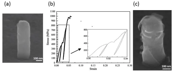
Figure 2.1b shows the stress-strain data for a representative conformally-coated nanopillar. The inset
provides a higher magnification of the initial 4% of deformation. Hysteresis loops can clearly be seen
during unloading/loading cycles while overall deformation up to failure remains nearly elastic with small
strain bursts present, and ultimately followed by a significantly larger burst. Post-deformation SEM
images (an example of which is given in Figure 2.1c) reveal that this large burst coincides with cracking
and subsequent delamination of the hard coating.
In order to investigate the effect of the hard coating in preventing dislocation escape through the free
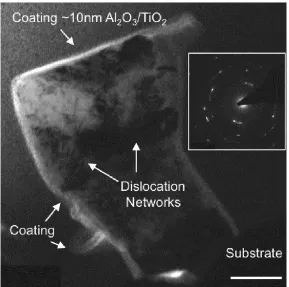
surface, we performed post-deformation TEM analysis. Figure 2.2 shows a bright-field TEM micrograph
of a representative nanopillar where the coating can be seen to have fractured off of the surface in
some areas. Imaging contrast show dense networks of dislocations that have built up in the interior of
the pillar. Streaking of spots seen in the inset diffraction pattern confirms the presence of significant
lattice deformation. The observance of a dense dislocation density is in contrast to previous findings on
sub-micron pillars that are generally characterized by a decrease in mobile dislocation density upon
deformation and lack such dislocation substructures [22]. This suggests that the presence of the
Al2O2/TiO2 coating is acting to prevent dislocation escape, causing dislocation pile-ups and the
subsequent development of dislocation networks.
Figure 2.1: (a) Pre-deformation scanning electron microscopy image of a conformally coated Cu nanopillar. (b) Compressive stress-strain data from coated Cu nanopillars. Inset shows high
[image:14.612.161.450.521.642.2]8
Figure 2.2: Post-deformation TEM micrograph of coating Cu nanopillar. Dense dislocation networks are observed within the pillar as pile-ups against the hard coating. The inset diffraction pattern shows streaking and is indicative of significant crystal deformation.
2.3 Analytic model for Bauschinger effect
In order to investigate the role of the coating as a source of hysteresis deeper within the pillar we
developed a simple one-dimensional analytical model based on dislocation theory that predicts the
emergence of hysteresis from dislocations piling up against the hard coating. Recent 3-D DD models on
coated nanopillars considered the cases of (1) an impenetrable coating and (2) dislocations capable of
breaking through the coating [23] and [24]. However, samples in these simulations were loaded
monotonically and thus did not explore the loading–unloading hysteresis. Similar 2-D simulations of thin
films with an impenetrable coating showed smooth hardening and a Bauschinger effect accompanied by
hysteresis loops [25] and [16]. Each of these studies incorporates varying aspects of the broad
[image:15.612.162.451.91.378.2]9
plane in isolation and employ classical dislocation theory to investigate compression of a coated
nanopillar. In contrast to dislocation dynamics-based models, this relies on solving the quasi-static
dislocation equilibrium configurations which do not rely on specification of mobility laws. In trade, this
serves as an approximate problem in the hope of offering a physical interpretation of the Bauschinger
effect. Hence, the aim of this model is not to act as an exact numerical comparison, but rather as a
physically founded qualitative complement to the experimental results.
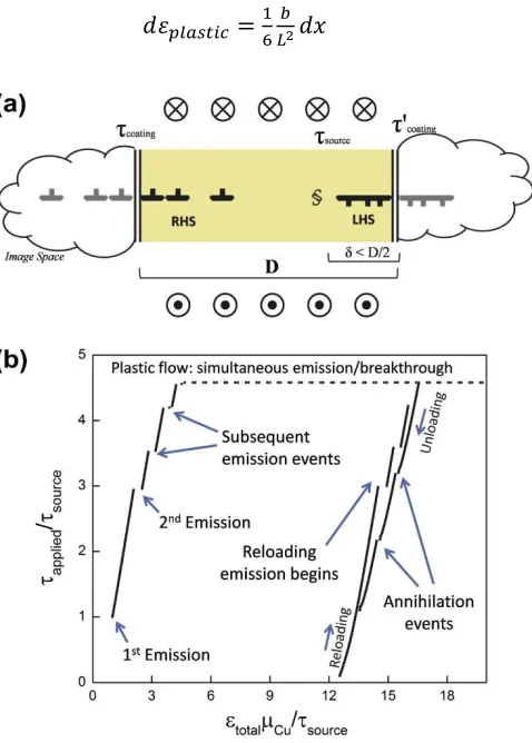
Starting with a cylindrical pillar, we isolated a resolved slip plane and considered it initially containing
only a dislocation source offset from the center with a given strength 𝜏𝑠𝑜𝑢𝑟𝑐𝑒. When activated, i.e., when the applied stress exceeds this strength, the source emits a dislocation loop, and has no short-range
interaction with the dislocations it emits throughout the simulation. Viewed along a cross-section of the
plane the resulting loop is seen as two oppositely oriented segments on either end of the slip plane, as
shown in Figure 2.3a. As this slip plane is isolated we do not consider interactions with other slip planes
or 3-D processes such as cross-slip. At the boundary of the domain is the coating with given strengths
𝜏𝑐𝑜𝑎𝑡𝑖𝑛𝑔 and 𝜏′𝑐𝑜𝑎𝑡𝑖𝑛𝑔 on either side, whose actual values may depend on elastic modulus or lattice mismatch, coating thickness, and orientation of the dislocation and interface [26]. Strengthening of
these collective interactions represents the Koehler barrier strength that sets a threshold stress at which
dislocations are allowed to pass through the coating [27]. Here we have taken 𝜏𝑐𝑜𝑎𝑡𝑖𝑛𝑔= 4
3𝜏′𝑐𝑜𝑎𝑡𝑖𝑛𝑔=
4𝜏𝑠𝑜𝑢𝑟𝑐𝑒, values comparable with those used in previous coated pillar simulations [23]. The difference in coating strength arises from the variation seen in coating thickness and possible variations in its bonding
strength that naturally arise during ALD deposition on a non-atomically smooth pillar surface. Figure
2.3a shows a geometrical diagram of the described set-up.
We take Cu as the representative materials and use it for all material properties. Beginning with the
10
±0.01𝜏𝑠𝑜𝑢𝑟𝑐𝑒. When the force concentrated at the source reaches 𝐹 = 𝜏𝑠𝑜𝑢𝑟𝑐𝑒𝑏, a loop is emitted and two oppositely oriented point segments are introduced into the slip plane at a distance 𝛿𝑥 = 0.2𝐿 on either side of the source, where L is the length of the slip plane. The equilibrium positions of these
dislocations are then determined through balance of the Peach-Kohler forces from long-range
dislocation interactions and image forces caused by the hard coating. As an approximation, we truncate
the image forces to the first image field. The Peach-Kohler force on the ith dislocation in a system of N
dislocations is given by:
𝐹𝑖 = 𝜏
𝑎𝑝𝑝𝑙𝑖𝑒𝑑𝑏 − 𝜇𝑏2
2𝜋 ∑
𝑠𝑖𝑔𝑛(𝑛,𝑖) 𝑥𝑛−𝑥𝑖 2𝑁
𝑛=1 𝑛≠𝑖
Eq. (2.1)
where we have treated the dislocations as screw-type, and where b is the Burgers vector and 𝑠𝑖𝑔𝑛(𝑛, 𝑖)
is read as the direction of the force on the ith dislocation by the nth dislocation. The summation is
performed over both the real and image dislocations for 2N total dislocations. Following the calculation
of the equilibrium position of the dislocations, the force on the two dislocations closest to the coating is
calculated to check if either exceeds their respective coating strength. This condition is:
𝜏𝑎𝑝𝑝𝑙𝑖𝑒𝑑− 𝜇𝑏 2𝜋∑
1 𝑥𝑛−𝑥1 𝑁
𝑛=2 ≥ 𝜏𝑐𝑜𝑎𝑡𝑖𝑛𝑔 Eq. (2.2)
If this condition is met, this dislocation escapes through the coating and the equilibrium positions of the
remaining dislocations are recalculated. If the condition is not met, then the applied stress is
incremented until the sum of the applied stress and the back-stresses are larger than the source
strength:
𝜏𝑎𝑝𝑝𝑙𝑖𝑒𝑑− 𝜇𝑏 2𝜋∑
1 𝑥𝑛 𝑁
11
This process is iterated through loading/unloading and at each stress, the total strain is calculated by the
elastic strain given by Hooke’s law and the plastic strain that is proportional to the distance swept out by
the dislocations:
𝑑𝜀𝑝𝑙𝑎𝑠𝑡𝑖𝑐= 1 2 𝑏
𝑉𝑑𝐴 Eq. (2.4)
For y indicating the direction normal to the plane and z directed out of Figure 2.3a, we can take a
representative volume, 𝑉 = 𝐿𝑥𝐿𝑦𝐿𝑧= 3𝐿2𝐿𝑧, with 𝐿𝑧being arbitrary for the 1-dimensional problem. With 𝑑𝐴 = 𝐿𝑧𝑑𝑥, the expression for plastic strain simplifies to:
𝑑𝜀𝑝𝑙𝑎𝑠𝑡𝑖𝑐= 1 6 𝑏
𝐿2𝑑𝑥 Eq. (2.5)
[image:18.612.187.426.289.623.2]12
directed into and out of the page are shown above and below the plane. (b) Shear stress normalized by the source strength vs. the dimensionless strain parameter generated by the analytical model with material properties representative of Cu, 𝜇𝐶𝑢 = 48 GPa and b = 0.256 nm.
Figure 2.3b shows the stress–strain curve resulting from the model, where the strain is a summation
across 10 identical slip planes. Starting with emission of the first loop, the loading curve is marked by
discrete events, each corresponding to source activation. This continues as the traveling dislocations pile
up against the coating. Eventually continuous plastic flow (with no hardening) begins, where the applied
stress is sufficiently high that both source emission and coating penetration occur simultaneously.
Plastic deformation continues until unloading, when the dislocations move back towards the center of
the domain and annihilate when two oppositely oriented dislocations are in proximity of each other. The
applied stress is then increased, and a clear deviation of the reloading curve from the unloading curve is
apparent. This hysteresis loop is only seen when a coating strength is applied at the boundary. In
exploring the virtues and limitations of this model we see that, as expected, the model shows no
difference in stress–strain curves between the unloading vs. reloading directions for the case of free
surfaces, which suggests that the Bauschinger effect is caused entirely by the presence of the coating.
While it is a necessary condition for the Bauschinger effect, it is not sufficient. Not just dislocation
storage, but asymmetric dislocation storage is sufficient to observe hysteresis. In simulations where the
dislocation source was placed directly in the center of the slip plane and the coating had equal strengths
on both sides, no hysteresis was observed. In this 1D model, asymmetric storage can be achieved
through differences in the coating strength. When break-through is achieved, dislocations on one side
will escape leaving their corresponding segment on the opposite side of the plane.
In contrast to earlier DD simulations on uncoated sub-micron copper-like pillars that exhibited a
Bauschinger effect [28], this model treats each dislocation source as independent, i.e., the dislocations
produced from one source do not interact with dislocations from a different source. As a result, during
13
strain curve from linear elasticity is a result of the emission and movement of dislocations (plasticity
gained) or relaxation and annihilation of dislocations (plasticity recovered). Considering an increase in
coating strength, more dislocations will be stored within the coating and thus greater deviation will
occur. We would then expect to see an increase in hysteresis with an increase in coating strength. These
modeling results are encouraging in that they appear to capture the behavior seen experimentally in a
model that is not computationally expensive and can be interpreted through classical dislocation theory.
2.4 Summary
In conclusion, uniaxial compression experiments on 75-1000 nm diameter electroplated single
crystalline Cu nanopillars coated with a conformal 5-25 nm layer of Al2O3/TiO2 displayed higher
strengths compared to as-fabricated counterparts. Hysteretic loops were observed during
unloading/reloading cycles whose magnitude increased with pre-strain. We have developed an
analytical model based on classic dislocation theory to investigate the emergence of the Bauschinger
effect in pillars with a hard coating. Hysteresis loops are observed in the data generated by the analytic
14
3. Strength and Deformation of Nano-scale Aluminum Containing a Single,
Vertically-Aligned Grain Boundary
3.1 Introduction
The development of nano-scale mechanical testing has led to insights in the plasticity of small-scale
crystalline metals of various microstructures including: nano-laminate [29,30], nano-twin [31,32], single
crystalline, and nanocrystalline microstructures [6,33]. The small sample volume lends itself well to
investigating the effect of isolated microstructural features on the deformation dominant mechanisms.
In contrast to single crystalline metals, nano-crystalline nanopillars of similar size and material show a
weakening, rather than strengthening with pillar diameter [6]. This reversal of mechanical behavior
highlights the importance that the microstructure has in determining mechanical properties at these
length scales.
Previous studies on cylindrical compression samples containing a single grain boundary have focused on
random grain boundary types oriented vertically within the cylinder [34–36]. Ngan et al. investigated
compressive response of 6 Al μm-diameter micro-pillars, each containing a general high-angle grain
boundary [34]. Transmission electron microscopy analysis revealed that the grain boundary was not
vertically-aligned as presumed, but extended at an angle from the top of the pillar to somewhere along
its mid-section. These authors noted substantial strain hardening in the compressive stress-strain
response of the Al bi-crystals, in contrast to single crystalline Al samples of equivalent diameters. They
also observed significant dislocation pileups near the grain boundary after the deformation, which
suggests that the grain boundary was acting as an obstacle to dislocation motion.
Kheradmand and Vehoff investigated compression of Ni pillars, each containing a vertically-aligned
15
These authors observed a 76–97% increase in yield stress compared with single crystalline specimens
only in the samples with diameters of 1.4–2 μm. Orientation Imaging Microscopy indicated that the
dislocation density in the vicinity of the grain boundary increased, which suggests that the grain
boundary acted as an obstacle to dislocation motion. The authors also observed slip transmission across
the grain boundary and a minimum density on slip bands where transmission occurred, which was
explained by the local rotation in the course of compression, which rendered the grain boundary no
longer an obstacle to dislocation motion.
Kunz et al. performed uniaxial compression experiments on a range of bicrystalline Al pillars, with
diameters spanning from 400 nm to 2 μm each containing a high-angle boundary oriented parallel to the
pillar and to the compression axis [35]. No significant hardening or distinctions from the single
crystalline samples of equivalent diameters were observed in the stress strain response of these
samples. TEM investigations displayed a low dislocation density near the grain boundary, more similar to
the density near the free surface than within the body of the pillar. They concluded that this particular
grain boundary likely absorbed the gliding dislocations and was acting as a sink for these defects.
This overview of the deformation of metallic micro-bicrystals demonstrates that for an isolated grain
boundary, both the orientation of the boundary with respect to the loading direction and the pillar size
can result in contrasting stress-strain response and microstructure evolution. Along with the five
degrees of freedom that specify the crystal orientation of the component grains and boundary
orientation, the atomic degrees of freedom play a role in the dislocation-grain boundary interaction
[37]. A lack of atomic information of the grain boundary configuration makes it difficult to compare
boundary behavior between samples.
Here we present the effect of a single, vertically-oriented coincident site lattice (CSL) grain boundary on
16
boundaries that contain a high number of well-known, coherent grain boundary sites. We also perform
molecular dynamics simulations on nanowire containing either a single high-angle or CSL grain
boundaries of known orientation to elucidate the atomic mechanisms that drive deformation. Portions
of this work were first published in Modelling and Simulation in Materials Science and Engineering [38].
Molecular dynamics simulations were performed by Garritt J. Tucker and Christopher R. Weinberger
(both now at Drexel University) at Sandia National Laboratories.
3.2 Grain boundary characterization and mechanical testing
3.2.1 EBSD Characterization
Compression samples were fabricated from a bulk sample of polycrystalline Al. The surface had been
previously smoothed by electropolishing and the grain size and texture had been analyzed by electron
backscatter diffraction. Using the grain orientation information and commercial Channel 5 analysis
software (HKL Research Inc.) we identified several highly symmetric grain boundary orientations. These
crystallites are related by one of the characteristic coincident site lattice rotations. In this bulk sample,
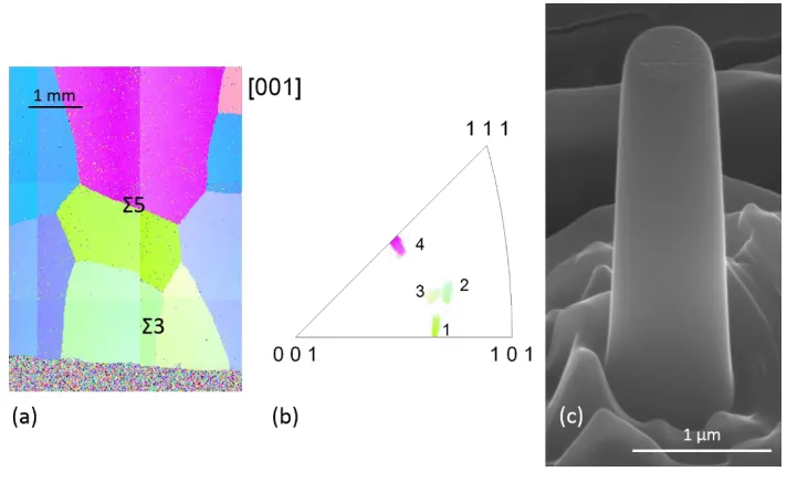
we have identified grain boundaries exhibiting a Σ3 and Σ5 CSL-type lattice. Figure 3.1a shows the grain
orientation map where the Σ3 and Σ5 boundaries are labeled and the individual orientations are given
on the stereographic triangle in Figure 3.1b.
3.2.2 Sample fabrication and compression experiments
Compression samples are fabricated within a dual-beam SEM (FEI) using the top-down focused ion beam
methodology [8]. A series of annular patterns with successively decreasing diameter were used to
remove material resulting in a cylindrical geometry. Ion milling was performed at 30 keV with decreasing
current from 3 to 0.05 nA. A representative compression sample is shown in Figure 3.1c. Compression
17
crystalline compression samples were also fabricated from within the bulk of each component
crystallite.
Uniaxial compression experiments were performed in a nanoindenter (Triboscope, Hysitron Inc.) using a
diamond flat punch tip with a diameter of 8 µm. Tests were performed under displacement-rate control,
at a nominal strain rate of 10-3 s-1. The displacement was monitored continuously at a frequency of 78
kHz via a feedback loop through the Hysitron performec control module. Engineering stress and strain
were calculated by dividing the force and displacement by the initial cross-sectional area and pillar
height, respectively. For comparison to previous studies, applied stress was resolved onto the slip
system with the greatest Schmid factor among both component grains and recorded at 7.5% strain. 19
nanopillars were tested along the Σ3 boundary and 10 nanopillars were tested along the Σ5 boundary.
Of these, 13 Σ3 nanopillars and 9 Σ5 nanopillars showed no evidence of bending or misalignment of the
indenter tip and were considered reliable tests.
Figure 3.1: (a) Crystal orientation map of grains used to fabricate compression samples. Grain
[image:24.612.130.486.409.627.2]18
3.2.3 Coincident site lattice
The coincident site lattice refers to the grain boundary lattice that results from points of coincidence
between the two crystalline lattices that compromise the grain boundary. The Σ-number is equal to the
inverse of the ratio of coincident sites to total sites. For example, Σ3 implies that 1 out of every 3 sites at
the grain boundary is a coincident site. Grain boundaries with low Σ-numbers therefore have a large
number of coincident points and relatively low energy in contrast to previous studies that have focused
nearly exclusively on high-angle, high-energy grain boundaries. The high number of coincident points in
low Σ-number boundaries also lends itself well to molecular dynamics studies, where the atomic
boundary structure can be easily modeled.
The Σ3 boundary is a special example of a highly-coincident boundary that is more commonly referred to
as a twin boundary. Previous reports on twin-dislocation interactions have investigated Cu nanopillars
containing twin boundaries spaced between 0.6-4.3 nm apart [31]. The authors observed that twin
boundaries can serve as sources of dislocations and can interact with impinging dislocations, forming
mobile Shockley partials capable of slipping on twin boundaries. Alternatively, transfer across Σ3
boundaries has been observed in Cu micropillars [39,40]. Suggested explanations include coherent slip
systems that allow for slip across the boundary [39] and transfer via cross-slip of screw dislocations [40].
3.2.4 Nano-scale compression experiments
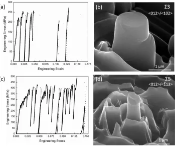
Figures 3.2a and 3.2c show post-deformation SEM images of a Σ3 and Σ5 pillar with their associated
stress-strain data. Stress-strain data in both types of grain boundaries is characterized by intermittent
bursts also frequently observed in similar compression tests on single crystalline metals [1,41]. These
bursts are attributed to dislocation avalanches released from their pinning points that get activated as
dislocation sources under applied stress [42,43]. These dislocations then freely travel across their slip
19
due to the discrete and stochastic changes in pillar geometry after yielding. Here we use the initial pillar
configuration as the reference geometry and, with respect to this initial geometry, no significant strain
hardening is observed in either Σ3 or Σ5 compression samples, suggesting the absence of barriers to
dislocation motion.
Figure 3.3 shows the resolved stress at 7.5% strain of CSL-containing compression samples plotted
against sample diameter. Also shown are resolved stresses at 7.5% of high-angle Al bicrystalline
nanopillars from Kunz, et al. [35]. Flow stresses for all samples increase with decreasing pillar diameter,
following the single crystalline trend [1,2]. The power law exponent for the size effect is identical in both
Σ3 and Σ5 nanopillars at 0.91 and is much greater than the exponent of high-angle GB Al bicrystalline
nanopillars at 0.58 [35]. Strengths match well with Al bicrystals from Kunz [35].
[image:26.612.136.485.356.646.2]20
It is not readily apparent whether the difference in power law exponent is due to the presence of the
CSL boundary or differences in initial dislocation density. A lower initial dislocation density in the CSL
bicrystals would result in an increased sensitivity to sample size. The stress-strain signatures of these
samples do not vary significantly from single crystalline Al and post-deformation SEM images show slip
planes traversing the boundary. These observations demonstrate that Σ3 and Σ5 boundaries do not act
as an obstacle to dislocation motion. Similar to reports in bicrystalline Cu micropillars [39], the presence
of coherent shear offsets that extend the entirety of the pillar diameter suggest the possibility of
matching slip systems that allow dislocations to pass through the boundary. Further analysis of the
crystallographic orientation information obtained from EBSD will be required to explore the possibility
of coherent slip systems.
[image:27.612.136.475.347.614.2]21
3.3 Molecular dynamics simulations
3.3.1 Methodology
Bicrystalline nanowires were constructed by generating a 3D periodic bicrystalline configuration
consisting of two crystalline lattices separated by a planar grain boundary. Employing an Al embedded
atom method (EAM) potential [44] and molecular statics, the total energy of the bicrystal was minimized
using a conjugate gradient scheme to create the initial grain boundary configuration. Prior to energy
minimization, numerous in-plane rigid body translations of one lattice relative to the other were
undertaken to better approximate the lowest energy configuration. From these bicrystals, a 30 nm
diameter cylinder was cut such that the grain boundary plane aligned parallel with the long axis of the
cylinder and was centered within the nanowire. Periodicity was maintained along the wire axis and free
surfaces were applied in the two transverse directions. Simulations were performed using the LAMMPS
molecular dynamics software package [45] and visualizations were generated using AtomEye [46] and
OVITO [47]. Simulations were performed at 300K and time integration of atomic position and velocity
was performed by sampling the isothermal-isobaric ensemble using a Nose-Hoover thermostat. We
studied three random high-angle grain boundaries and a series of symmetric tilt boundaries. Figures
3.4a and 3.4b show side and axial views of the generated high-angle bicrystal. Atoms in Figure 3.4b are
colored by their centrosymmetric value [48] and undisturbed atoms have been removed for clarity.
Figure 3.4c provides a stereographic triangle with the orientations of the three high-angle bicrystal
systems studied.
Compression was induced by decreasing the periodic dimension of the simulation box at a nominal
strain rate of 108 s-1 up to a final 20% engineering strain. Stress was calculated every 5 ps following the
atomic virial stress definition:
𝜎𝑖𝑗 = 1
𝑁Ω∑ ∑ 𝑓𝑖
𝛼𝛽 𝑁𝛼
𝛽≠𝛼 𝑟𝑗
𝛼𝛽 𝑁
22
where Ω is defined as the atomic volume, N represents the total number of atoms in the system, 𝑁𝛼
represents the number of neighboring atoms for each atom α, 𝑓𝑖𝛼𝛽 defines the interatomic force vector between each atom α and its neighbor β in the i direction, and 𝑟𝑗𝛼𝛽 is the interatomic distance of atoms
α and β in the j direction. The common neighbor analysis method was performed along with stress to
compute the local crystal structure of each atom.
Figure 3.4: (a) Side view of bicrystalline nanowire generated for MD simulations. (b) Axial view of bicrystalline nanowire. Atoms are colored based on their centrosymmetric parameter and inner lattice atoms have been removed for clarity. (c) Stereographic triangle showing the crystal orientations of the three simulated high-angle bicrystal systems.
3.3.2 Results
3.3.2.1
High-angle grain boundaries
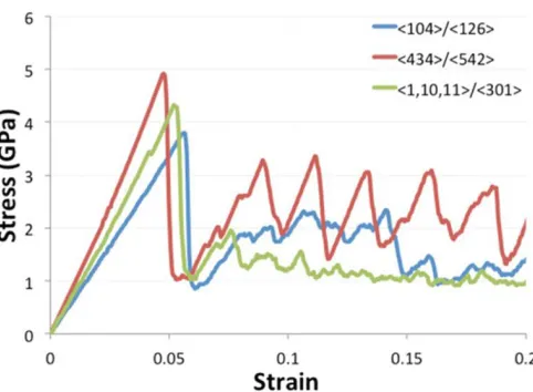
Figure 3.5 shows the stress-strain data generated from compression simulations on 3 different
bicrystalline nanowires. All 3 nanowires reach approximately the same peak stress, but display differing
[image:29.612.195.423.219.499.2]23
Figure 3.6a shows an axial cross section of a nanowire at 5% strain. Atoms are colored by their crystal
structure as determined from common neighbor analysis (CNA) [49,50]. The initial dislocation nucleation
event shown in Figure 3.6a occurs within the high-symmetry crystallite and occurs at the intersection of
the interface and surface. After initial nucleation, the dislocation travels through the crystal, depositing
Burgers vector content into the boundary, which is behavior consistent with the GB acting as a sink.
Unimpeded dislocation glide results in dislocation starvation, where additional dislocations must be
nucleated to accommodate the applied strain. This mechanism of additional nucleation leads to the
stick-slip behavior seen in the stress-strain <434>/<542> bicrystal. If migrating dislocations are instead
momentarily trapped by lattice defects or there is the presence of a mechanism that more easily
nucleates new dislocations, the plastic behavior appears smooth, like that seen in the <1,10,11>/<301>
bicrystal. In these nanowires, twin boundaries are observed that serve as preferred nucleation planes
and paths for dislocations and requires lower axial stress to nucleate new dislocations. This decreased
nucleation stress and preferred slip path contributes to a smoother post-elastic stress-strain signature.
At high compressive strain, after several lattice dislocation interactions and absorption events, full
dislocation loops are seen to nucleate from the GB into the lattice. Figure 3.6b shows the same
cross-section as seen in Figure 3.6a at a high compressive strain, where dislocations loops can be seen
nucleating from the GB on the {111} slip planes. In all three high-angle bicrystalline nanowires, there
was no evidence supporting the GB acting as an obstacle to migrating dislocations. No dislocation
pile-ups or pinned dislocations were observed near the GB for long periods of time. All lattice dislocations
24
Figure 3.5: Compressive stress-strain data for all high-angle bicrystalline nanowires. Peak stress is similar between all bicrystals while plastic stress varies from stick-slip behavior to smooth deformation.
Figure 3.6: (a) Axial view of the initial nucleation event. Emission occurs at the intersection of the GB and the free surface. (b) Nucleation of full dislocation from the GB into both crystals is observed after significant deformation. All atoms are colored by their CNA value and FCC atoms are removed for clarity.
3.3.2.2
Symmetric-tilt grain boundaries
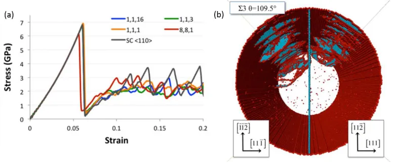
Figure 3.7a summarizes the stress-strain data generating from compression simulation on a bicrystalline
nanowire containing a symmetric-tilt grain boundary. Boundaries studied include Σ129, Σ11, and Σ3. The
interface has negligible effect on the stress of the initial nucleation event. The single-crystalline (i.e., 0°
tilt) displays stick-slip plasticity due to dislocation exhaustion. All other symmetric-tilt bicrystalline
[image:31.612.184.425.77.254.2] [image:31.612.148.465.318.484.2]25
and then emitted from <100> surface facets. In both low and high-angle symmetric structures, the
interface acts as a sink for incoming dislocations. Any impedance of the dislocation motion by the GB is
temporary. Dislocation pile-ups were not observed during compression.
Figure 3.7: (a) Compressive stress-strain data for all symmetric-tilt bicrystalline systems. (b) Axial view of nucleation within Σ3 nanowire. Nucleation occurs from the free surface within both crystals.
Figure 3.7b shows the initial nucleation event in the Σ3 nanowire. In the case of the Σ3 nanowires, the
boundary would absorb the incoming dislocation to create a GB or twin dislocation. Subsequently,
emission of a full dislocation into the opposite lattice and back into the original lattice on the incoming
{111} plane returns the Σ3 boundary to its low energy structure. This demonstrates an
energetically-favorable mechanism in Σ3-containing nanowires that allows for transmission of dislocations across the
grain boundary without significant deformation of the boundary, a conclusion consistent with the
experimental observance of slip traces traversing the grain boundary.
While a single EAM potential was used in this study, it has been observed that the potential can affect
the activation energy for diffusion in Al Σ5 boundaries [51]. In the high-angle grain boundaries, this could
lead to differences in atomic migration along the grain boundary and thus distribution of Burgers vector
content absorbed from migrating dislocations. In the symmetric-tilt grain boundaries, this could play a
[image:32.612.114.503.162.325.2]26
3.4 Summary
In summary, we performed compression experiments on Al bicrystalline nanopillars containing a single
CSL grain boundary of either a Σ3 or Σ5 character. Stress-strain data was similar to single crystalline data
and did not display any evidence of mechanisms that impeded dislocation motion. Post-deformation
SEM images revealed slip traces that passed through Σ3 CSL grain boundaries. The CSL grain boundaries
did not appear to have an impact on the size effect, displaying similar scaling to single crystalline
samples. We also performed molecular dynamics simulations on bicrystalline nanowires containing a
single random grain boundary and nanowire containing a symmetric-tilt grain boundary. Random grain
boundaries were observed to initially act as a sink to dislocations and a source of dislocations with
further straining. Symmetric-tilt grain boundaries did not act as boundaries to dislocation, but absorbed
incoming dislocations and emitted dislocations into both component crystals. No dislocation pile-ups
were observed in either random or symmetric-tilt grain boundaries. The grain boundaries do not act to
impede dislocation motion and can function as dislocation sources or allow dislocation transmission, as
27
4. Room Temperature Grain Boundary Sliding in Nano-scale Aluminum
4.1 Introduction
Grain boundaries in crystals present an intriguing mystery in the materials sciences because of a paucity
of reports on their atomic structure, morphology, and deformation properties. Multiple studies indicate
that at high temperatures the grain boundaries slide past one another to carry plastic strain, while at
room temperature deformation is dominated mainly by dislocation motion and their interactions with
the grain boundaries. The limited number of experimental reports on the energetic and structural
landscape of grain boundaries renders modeling of the general grain boundaries a particularly
challenging task. Most of the existing literature is focused on well-defined, special boundaries such as
symmetric tilt or pure twist boundaries [37,52–54].
The development and extensive use of the uniaxial micro- and nano-pillar uniaxial compression
methodology has allowed for studies on metallic nanopillars with a variety of microstructures including:
single crystalline, nano-twinned [31], nano-crystalline [6,33], bi-crystalline [34,35], and amorphous
metallic glasses [55], each exhibiting unique mechanical behavior. A main finding from the uniaxial
deformation experiments on single-crystalline metallic micro- and nano-sized samples is the emergence
of a power law dependence of their flow stresses on sample dimensions [1,2]. This is in contrast to the
classical theory, which dictates crystalline strength to be independent of sample size. The size effect in
the nano-sized single crystals was attributed to the plasticity mechanism being dominated by
dislocations nucleating either from single-arm sources [4,13,14] or from surface sources [5,15,56] rather
than by dislocation multiplication, as in bulk [12]. In contrast to the single crystalline metals, the
nano-crystalline nanopillars of similar size and material show a weakening, rather than strengthening, with
pillar diameter. This reversal of mechanical behavior highlights the importance that the microstructure
28
Reported experiments on bicrystalline micro- and nano-pillars have concentrated on random, high-angle
or CSL-type grain boundaries that are oriented vertically or at an angle from the pillar axis [34–36].
Deformation in these pillars was accommodated by dislocation activity and no significant movement of
the grain boundary was observed during compression. Interactions between dislocations and the grain
boundary were seen to differ between grain boundaries and possibly dependent on the orientation of
the boundary with respect to the loading direction and pillar size. This limited loading configuration
results in no shear stress acting across the grain boundary and limits the available deformation
mechanisms. The lack of investigation into the mechanical behavior of isolated grain boundaries under
more varied loading configurations limits the current understanding of grain boundary deformation
mechanisms because such axial loading results in no shear stresses acting along the grain boundary.
We conducted room-temperature uniaxial compression experiments on bi-crystalline Al nanopillars with
diameters of 900 nm, each containing a single grain boundary, whose plane normal was inclined at an
angle of approximately 24–28° from the loading direction. This orientation was intentionally chosen to
subject the grain boundary to applied shear loading, in contrast to nearly all existing reports on the
deformation of small-scale metallic bi-crystals. We observed the deformation to commence via a
gradual sliding process along the grain boundary, where the top crystallite sheared off as a single piece
with respect to the bottom one, with no evidence of any other significant plastic deformation. The
stress-strain response contained an initial peak at a strain of 1%, which corresponded to the initiation of
the shear offset, and a subsequent softening followed by a decrease and increase in stress between 79–
112 MPa over 12% compressive strain. The data was continuous, showing no stochastic bursts. TEM
analysis revealed no apparent dislocation debris at the grain boundary. We also performed molecular
dynamics compression simulations on bicrystalline nanopillars containing a single tilted grain boundary
at a tilt angle between 0° to 55° from the pillar axis and shearing simulations on a planar grain boundary.
29
deformation with increasing tilt angle. Shearing simulations show qualitatively similar stress-strain
signatures and reveal a mechanism of atomic migration that facilitates grain boundary sliding.
4.2 Experimental
4.2.1 EBSD characterization and sample fabrication
Samples were prepared from a block of high purity aluminum poly-crystal that had been previously
annealed under vacuum at 350 °C overnight, followed by electro-polishing. Pillars were carved using a
subtractive etching methodology in the Focused Ion Beam (FEI Nova 600) [8]. Electron backscatter
diffraction (EBSD) was used to characterize the location of the grain boundary and orientation of each
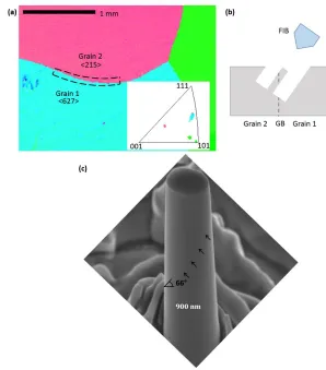
grain. Figure 4.1a shows an orientation imaging microscopy (OIM) crystallographic map of the crystal
face from which the samples were fabricated, with the specific boundary studied denoted by the dashed
rectangle. In contrast to the typical top-down fabrication methodology of vertically-oriented pillars
utilized by multiple research groups [5,8,42,57,58], here (once a suitable boundary was located) the
sample stage was tilted within the chamber such that the surface normal was inclined at 35° relative to
the ion beam column and the pillars were milled using an annular pattern. The inner diameter of the
final annulus was 1 μm, resulting in a typical actual pillar diameter of ∼900 nm, with the final pillar height maintaining an aspect ratio (height/diameter) between 3:1 and 4:1. The inclination between the
samples surface normal and the ion beam led to the non-orthogonal orientation of the pillar tops with
respect to the pillar axis. The sample was then rotated by 180° within the chamber and inclined such
that the ion column was perpendicular to the pillar axis. Utilizing a rectangular milling pattern, the
inclined pillar top was flattened (Figures 4.1b and 4.1c). A SEM image of a representative sample with a
tilted grain boundary is shown in Figure 4.1c, where the grain boundary can be seen extending from
30
Figure 4.1: (a) Orientation Image Microscopy map generated by EBSD, which shows 3 grains in the top surface of the bulk Al crystal. The region along which the pillars were made is indicated by the bashed boundary. The inset shows the stereographic triangle with the grain orientations of <627> and <215>. (b) Schematic of the FIB milling process where the ion beam is tilted 35° from the sample surface normal. (c) A representative pillar (∼900 nm diameter) containing a grain boundary inclined 66° above horizontal. The arrows below the boundary trace its path along the pillar surface.
Compression testing of all pillars was performed in a nanoindenter (Triboscope, Hysitron Inc.) using a
diamond flat punch tip with a diameter of 8 μm. The tests were conducted under displacement rate
control, at the nominal strain rate of 10−3 s−1 up to 15% total strain. The displacement was monitored
continuously at a frequency of 78 kHz via a feedback loop through the Hysitron performec control
module. True stress and true strain were calculated from the measured load and displacement data by
following the methodology [8] and were corrected for the machine and the substrate compliances, as
[image:37.612.143.441.72.411.2]31
wedge sample holder that rotated the sample in order to orient the axis of each tilted pillar parallel to
the indenter column. 7 nanopillars were constructed along the boundary although the orientation of the
grain boundary within the nanopillar prior to compression could only be verified through SEM imagining
within 2 of these samples.
Analysis of microstructure in the deformed samples was performed via transmission electron
microscopy (FEI, Tecnai F30) at an accelerating voltage of 300 kV. Samples were lifted out from the
parent crystal using a micromanipulator within the FIB (Omniprobe, Inc.) and attached to a TEM grid
with ion-beam assisted, site-specific, Pt deposition. Once attached to the TEM grid, the samples were
thinned using decreasing current down to 10 pA to a thickness of <100 nm to ensure electron
transparency.
4.2.2 Compression experiment results
Figure 4.2b displays compressive stress-strain data for a representative 900 nm diameter sample. The
plot shows that elastic loading led to a maximum axial stress of 156 MPa, after which the stress
decreased abruptly to 100 MPa at the strain of 2.5%, slightly increased up to 112 MPa at 4.2% strain,
and then gradually decreased to 79 MPa at 14% strain before rising to 100 MPa at the unloading strain
of 16.2%. The data appears to contain some high-frequency oscillations after the local minima in stress
at 2.5% strain and does not exhibit strain bursts typically seen in micron- and nano-scale pillar
compression tests [41].
Figure 4.2c shows the post-deformation SEM image of this sample and reveals that virtually all plastic
deformation was carried out by a single shear offset at a tilt angle of 66° from the horizontal. The
created surface formed along the grain boundary (Figure 4.2c). Examining the sheared off regions
32
3 nanopillars. Earlier work on uniaxial compressions of similarly fabricated bi-crystalline Al cylinders of
equivalent diameters, which contained a high-angle grain boundary oriented along the compression
direction, exhibited substantially different response, including post-elastic hardening, stochastic
stress-strain signature, and significant crystallographic slip [35]. This highlights the influence of grain boundary
orientation with respect to the loading direction on the deformation mechanism: the frictional sliding of
the top grain occurred only in those bi-crystals, where the grain boundary experienced applied shear
stress.
Figure 4.2: (a) SEM image of an as-fabricated pillar before uni-axial compression with the direction of applied load shown by the black arrow. (b) Stress-strain data of the same pillar collected during the compression experiment. Yield corresponds to the maximum peak stress at the strain of 0.5%, after which it rapidly softens, and plastic flow commences at a gradually decreasing stress to the final
unloading strain of ∼16%. The compressive stress-strain data of Kunz et al. [35] of bicrystalline Al pillars with equivalent diameters, each containing a vertically-aligned grain boundary, is provided for
comparison in the inset (reprinted with permission from Elsevier). In contrast to the compressive data generated for the slanted-boundary pillars in this work, stresses in the vertical-boundary samples exhibited significant hardening and pronounced stochastic behavior. (c) Post-deformation SEM image of the same pillar taken along the same directions as in (a), which shows that the upper grain sheared off from the lower grain along the grain boundary plane. Wavy features can be seen on the exposed grain boundary plane extending periodically from the near side of the pillar to the far side. Inset in the upper right corner shows a top-down view of the same pillar. All SEM images shown were taken at a 52° tilt angle between the sample surface normal and the electron beam.
The shear stresses acting along the grain boundary were calculated by resolving the measured applied
axial stress onto the grain boundary plane in the direction of the offset. This corresponds to a
[image:39.612.78.537.272.424.2]33
of 0.372. This translates to a maximum resolved shear stress of 58 MPa and corresponds to the axial
peak stress of 156 MPa at the strain of 0.5% and the average resolved shear stress of 36 MPa, computed
by averaging over 120,000 data points between 2.4–16.2% strain. This maximum resolved shear stress is
39% lower than the shear stress at 7.5% strain resolved onto the principle slip system of 95 MPa
reported for the bi-crystalline Al nano-pillars with a vertically oriented grain boundary [35]. The stiffness
measured from the initial 15% of the data in the elastic unloading segment was 57 GPa, a value 25%
lower than expected from theoretical calculations. The stiffness measured from tilted single crystalline
pillars fabricated from grain 2 and did not contain a grain boundary was 66 GPa, a value within the range
of measured stiffness seen in Al bi-crystalline pillars containing a vertical boundary [35]. The lower
unloading stiffness measured for the pillars that deformed by sliding is likely a result of the reduced
cross-sectional area as the top crystallite shears off, which may not be representative of the actual
elastic modulus of the material.
4.2.2 Discussion
The first striking difference between the compressive stress-strain curves of the tilted-boundary pillars
studied in this work and similar curves for the single crystalline and vertically oriented bi-crystalline
samples is their continuous signature with almost negligible strain bursts. This is markedly different from
the typical compressions of the single-crystalline and vertical grain boundary-containing bi-crystalline
nano-metals, whose stress-strain signature is stochastic and populated with numerous strain bursts that
range from 1 nm to ∼100 nm [2,59]. These bursts have generally been attributed to the initiation and propagation of avalanches of dislocations being released from their pinned locations and/or from
dislocation sources [42,43]. The lack of such stochastic behavior and of noticeable crystallographic slip
lines in the tilted-boundary nano bi-crystals suggests that when shear stresses are applied to the
boundary, the deformation mechanism becomes distinctly different from the dislocation
34
The axial stress peaks at 156 MPa attained immediately after the elastic loading, which corresponds to a
58 MPa shear stress resolved onto the grain boundary plane in the direction of sliding, approximately a
(111)/[011̅] system. The observed subsequent softening is initially abrupt to ∼2.5% strain and is more gradual thereafter. This may physically correspond to the initiation of the shear offset at peak stress,
followed by an abrupt drop in stress due to the inertia of the initial sliding and a deceleration at 2.5%
strain, where the sliding becomes comparable to friction, and the deformation continues at a steady
state. This sharp decrease in stress caused a momentary rise in the displacement rate, until the
prescribed rate was re-established via the feedback loop algorithm in the nanoindenter software.
The primary slip system under compression for the upper grain (grain 1) is (1̅1̅1)/[101], whose Schmid factor is 0.481. Although the boundary plane for grain 1 is of {111} type, the TEM image in Figure 4.3b
reveals that it does not correspond to the primary slip system, which is denoted by the white arrow.
In the HRTEM image (Figure 4.3c), the set of parallel (111) planes align with the grain boundary,
evidenced by the fringes in the upper grain. These planes terminate within the grain boundary and can
be considered as ‘extra’ planes, or edge dislocations with a Burgers vector of √3. A lack of distortion of the fringes near the grain boundary suggests that little, if any, strain has accumulated in the vicinity of
the boundary, likely due to the interrupted compatibility, or decohesion, between the crystallites after