E THE R LIN X P L U S
3 C 5 0 5
D EVE LOP E R I S
Revision 3.0 3Com Corporation
May 2.1, 1986
PREFACE
This document is intended for use by sophisticated software engineers who will either be writing application software that will talk to the 3C505, or software that will actually reside on the card. The user is expected to have a strong background in microcomputer systems. It is recommended that the user browse through the Intel 80186 Data Sheet and the Intel Lan Components User's Manual before beginning (they are available through Intel).
The manual is divided into the following chapters:
CH1~PTER 1
CHAPTER 2
CHAPTER 3
APPENDIX A
APPENDIX B
APPENDIX C
HARDWARE EXTERNAL REFERENCE SPECIFICATION (ERS) Provides a description of the 3C505 architecture, system resources and functional operation.
HARDWARE INTERFACE SPECIFICATION
Describes the programmable registers used to control, configure, and communicate with the 3C505.
COMMAND INTERFACE SPECIFICATION
Describes the function and use of the command level interface software supplied with the card. 80186 PERIPHERAL CONTROL BLOCK PROGRAMMING
Provides the values used in the 3C505 firmware to configure the 80186 internal resources.
82586 CONFIGURATION
Provides the values used by the 3C505 firmware to configure the 82586.
3CSOS DIAGNOSTIC
Describes the operation of the 3C505 diagnostic utility program.
3D DEBUGGER
TABLE OF CONTENTS
CHAPTER 1 - HARDWARE EXTERNAL REFERENCE SPECIFICATION 1.0 1.1 1.2 1.3 1.4 1.5 1.6 1.7 1.S 1.9 1.10 1.11 1.12 1.13 1.14 1.15 Introduction Resources Architecture Address Maps
1.3.1 Adapter I/O map 1.3.2 Adapter memory map 1.3.3 Host I/O map
80186 Microprocessor
82586 Ethernet Coprocessor Network Interface
1.6.1 82586 Serial Interface 1.6.2 8023 Manchester Converter 1.6.3 Transceiver
Adapter Firmware ROM Adapter RAM
Host-Adapter Interface 1.9.1 Command Register 1.9.2 Data Register
1~9.3 Data Register configuration 1.9.4 DMA Transfers
1.9.5 Status Flags Adapter Interrupts
1.10.1 Internal Interrupts 1.10.2 External Interrupts Host Interrupts
Resetting the Adapter Ethernet Address
LED Indicators Host ROM
CHAPTER 2 - HARDWARE INTERFACE SPECIFICATION 2.0 2.1 2.2 2.3 2.4 2.5 2.6 2.7 Introduction Conunand Register Data Register
Host Control Register Host status Register Host Aux DMA Register Adapter Control Register Adapter status Register
Page #
CHAPTER 3 - COMMAND INTERFACE SPECIFICATION 3.0 Introduction
3.1 Primary Command Block structure
3.1.1 status Flag Usage for PCB Transfer 3.1.2 Host to Adapter Request
3.1.3 Adapter to Host Request or Response 3.2 PCB Commands
3.2.1 Host to 3C505 PCB Formats 3.2.2 3C505 to Host PCB Formats 3.3 System ROM Utilities
3.3.1 Host I/O support: INT SOH 3.3.2, Network I/O S~·;,>,\:i"rt~ INT SlH 3.3.3 Configuration/S\ ~lS. INT 82H 3.3.4 Timer Support: INT 83H
3.3.5 Download Program Support: INT 84H 3.3.6 PCB Command Processor: INT 85H 3.3.7 Packet Processor vector: INT 86H 3.3.8 Idle Vector: INT 87H
3.3.9 PCB Enqueue Vector: INT 8SH
LIST OF FIGURES
APPENDIX APPENDIX APPENDIX APPENDIX
A~PENDI:X
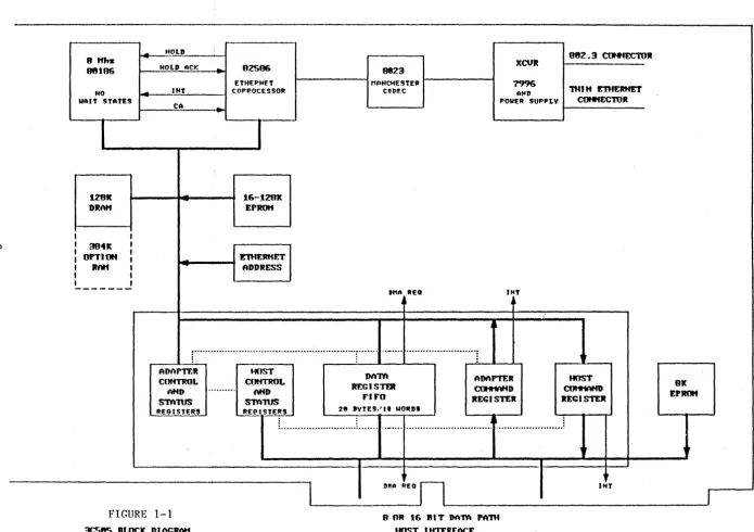
Fiqure 1-1: 3C505 Elock Diagram Figure 1-2: DRAM Refresh
A - 80186 PERIPHERAL CONTROL BLOCK PROGRAMMING B - 82586 CONFIGURATION
C - 3CSOS DIAGNOSTIC D - 3D DEBUGGER
E 3C50S" DEVERLOPER' S SOFTWARE DISKETTE '
28 28 30 30 31 32 32 37 41 41 44 45 47 48 49 50 51 51
2
8
CHAPTER 1
HARDWARE EXTERNAL REFERENCE SPECIFICATION
1.0 INTRODUCTION
The EtherLink Plus, 3C505, is a high performance Ethernet
adapter for IBM PCs and compatibles. It consists of an 80186 16
bit microprocessor, an 82586 Ethernet coprocessor, up to 512K
bytes of user RAM, a high speed 16 bit host interface, and a
highly integrated on-board transceiver. The 3C505 is
particularly well-suited for server and high performance
workstation applications.
1.1 RESOURCES
• 8 Mhz 80186 16 bit microprocessor - no wait states
*
82586 multi-packet buffer Ethernet coprocessor*
16K to 128K bytes EPROM• 128K to 512K bytes packet buffer/program memory
*
8/16 bit host interface - PIO or DMA*
20 byte FIFO to maximize host/adapter data transfer*
On-board "Thin Ethernet" transceiver/802.3 connector*
8K bytes host EPROM1.2 ARCHITECTURE
The 3C505 is a 16 bit microcomputer with a high performance
Ethernet I/O channel and an IBM PC AT interface. The 16K bytes
of on-board firmware contain software that supports',
initialization, program download, and diagnostic software. The
128K RAM, expandable to 512K, allows for protocol processing a.s
well as offloading of application programs from the host PC. The
82586 performs all Data Link functions, as well as powerful:
network diagnostics. It performs all packet buffer management
functions and, in a typical environment, will not "drop" packets.
The host interface supports high speed, 8 or 16 bit, DMA
transfers as well as programmed I/O. The interface is very
flexible, yet simple, allowing for easy programming. The 8 Mhz
N
8 tfhs
88UJ6
NO ..,An stAtES
I
1291( DRAH
I I
I 3941C , : OPTIOtt : I RNt ,
, I
,
---
,
--
HOLDHOLD ACt:
-INt
CA
-0259G ETHEPNET COPROCESSOR
16-120X EPROH
~---~ ETHERHF.T
ADDRESS
9123 t1ttNCHE'TER
COllEC
'"A REQ
XCUR
7996
AND POIIER SUPPLY
[image:6.797.39.735.93.583.2]IHT
... _ ... .
·
.
·
.
·
082.3 COHHECTOR
1.3 ADDRESS MAPS
1.3.1 ADAPTER X/O MAP
HEX Address
o
100
Byte/Word NA (see text) Low Byte
Description 82586 CA 102 102 102 104 180-18F FFOO-FFFF
Low Byte Read High Byte Read High Byte write Word
Adapter Command Register Adapter Control Register Adapter status Register Adapter Control Register Data Register
Low Byte Wo-:r:d
1.3.2 ADAPTER MEMORY MAP HEX Address
OOOOO-lFFFF 20000-3FFFF 40000-5FFFF 60000-7FFFF FCOOO-FFFFF EOOOO-FFFFF
Ethernet address (6 Bytes) Peripheral Control Block
Description
128K Bytes system RAM: Bank 1 128K Bytes option RAM: Bank 2 128K Bytes option RAM: Bank 3 128K Bytes option RAM: Bank 4 16K Bytes system ROM
*
128K Bytes system ROM (If 27512s are installed)
*
Address lines A20-A23 of the 82586 are ignored and the Initialization Root is located at FFFF6 in system ROM.1.3.3 HOST Z/O MAP
HEX Address (factory set)
**
Base address + 0 (300)Base address + 2 (302) Read Base Address + 2 (302) write
Base address + 4 (304)
Base address + 6 (306) Read
Description
Host Command Register Host status Register Host Control Register Data Register
***
Host Control Register**
The address is given as an offset from the I/O base address which is set using the I/O address jumpers on the card. The factory set base address is 300H.***
The slot(AT).
Data Register is a byte wide register in an 8 (PC, XT, or AT) and word wide in a 16 bit
1.4 80186 MICROPROCESSOR
The 3C505 uses the Intel 80186 Microprocessor. This is a highly integrated 16 bit processor with 3 timers, 2 DMA channels, and an interrupt controller on chip. The 80186 is software compatible with the 8086.
The 80186 timing is generated by a 16Mhz crystal. An internal divider generates an 8Mhz clock output which is used for system timing. All 80186 bus cycles are 4 clock cycles long, or 500 nanoseconds, with a system memory bandwidth of 2 Megawords per second. All DMA transfers require 2 bus cycles, or 1 microsecond.
1.5 82586 ETHERNET COPROCESSOR
The 82586 is a high performance, intelligent communications processor resRonsible for all network related tasks, including frame reception and transmission, error logging, and diagnostics. The 82586 has two interfaces: a parallel system bus interface to communicate with the 80186 and to retrieve and store packet data in system RAM; and a serial interface to transmit and receive data from the network. The serial interface is described in section 1.6, Network Interface. The 82586 bus interface operates from the 8 Mhz system clock and all bus cycles are 500 nanoseconds.
The 80186 and the 82586 operate in a shared bus configuration using the HOLD/HOLDA protocol. This configuration is described in detail in the Intel Lan Components User's Manual. In this mode, only one of the processors can use the system bus at a time. All interprocessor communications are via the system RAM. The 80186
can initiate a transaction by asserting the CA (Channel Attention) input to the 82586. A read or write to I/O location
00 will cause an active transition on the CA input. The 82586 initiates a transaction by asserting the 80186 INT1 input.
~.6 NETWORK INTERFACE
The 3C505 network interface consists of the serial interface
the Intel 82586 LAN controller, the SEEQ 8023 Manchester
Converter, and an on-board transceiver using the AMD
Transceiver IC.
~.6.1 82586 SERIAL INTERFACE
on Code
7996
The 82586 perfo~s all parallel to serial and serial to
parallel convers~on during packet transmission and
reception. During transmit, parallel data is retrieved from
the Adapter RAM through the 82586 bus interface. The 82586
serializes the data, inserts the preamble, source and
destination fields, appends a CRC field to the "packet", and
outputs the bit stream. The 82586 also performs the CSMA/CD
link management algorithm according to the IEEE 802.3
standard. During reception, the 82586 strips off the
preamble and compares the destination address field with the
station address to see if the frame should be received. If
so, the serial bit stream is converted into bytes and stored in the Adapter RAM.
1.6.2 8023 MANCHESTER CONVERTER
The 8023 is responsible for the Manchester encoding and decoding of the serial bit stream between the 82586 and the
transceiver. It also supplies the transmit and receive
clocks to the 82586 serial interface. A watchdog timer on
the IC prevents continuous transmission of more than 25
milliseconds, thus limiting the maximum packet size to
approximately 3lk bytes.
For diagnostic purposes, the 8023 can be placed in "loopback
mode" whereby the transmitted data is internally routed to
the receive section. This is useful for isolating
transceiver problems. Enable loopback by clearing the
Loopback bit in the Adapter Control Register. Refer to the
3C505 Hardware Interface Specification, Chapter 2.
~.6.3 TRANSCEIVER
The 3C505 onboard transceiver physically connects the 3C505
to the "Thin Ethernet" coax cable. It performs the
necessary signal conditioning as well as collision
The user can also connect the 3C505 to a thick Ethernet network through an external transceiver such as the 3Com 3CI02. If so, the user must disable the onboard transceiver and enable the 15 pin connecter on the backplate of the card. To do so, the transceiver select plug in the card must be moved from the BNC position to the DIX position. The EtherLink Plust Installation Guide, included with the 3C505, illustrates this procedure.
:1,,7 ADAPTER FIRMWARE ROM
The 3C505 contains 16K bytes of firmware contained in two 8Kx8, 2764 type ROMs. These ROMs can be replac~d by 27128, 27256, or 27512 ROMs for up to 128k bytes of firmware. The ROMs must have a maximum address access time of 250 nanoseconds or less.
The 3C505 ROM firmware performs self-test, initialization and configuration, and DRAM refresh. It also provides, through a command block interface, a set of functions which support Host/Adapter I/O, network interfacing and execution of downloaded programs. Refer to the 3C505 Command Interface Specification, Chapter 3, for more details.
The system ROM is mapped to address space FCOOOH-FFFFFH (EOOOOH-FFFFFH if 128k bytes are used) and is accessible to both the 80186 and 82586. The 82586 only accesses ROM following an 82586 reset to fetch the initialization root.
1.8 ADAPTER RAM
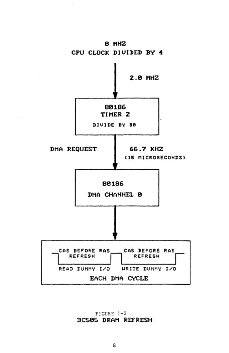
Software must perform two functions for proper RAM operation: initialization and refresh. To refresh the RAM, 256 consecutive locations in each bank must be accessed every 4 milliseconds. Data loss will occur if refresh is not performed. The initialization procedure depends on the refresh technique used. To facilitate refresh, the 3C505 contains hardware which utilizes the "CAS before RAS" refresh feature of the DRAMs. In this mode, the RAMs generate the refresh address internally after each CAS before RAS cycle, and the internal address counter increments so that the next CAS before RAS cycle will refresh the next address. A read or write to I/O location 80H will produce a CAS before RAS cycle in all banks simultaneously. The 80186 PCSl Peripheral Chip Select output is programmed for this range. NOTE: A CAS before RAS cycle, read or write, does not corrupt RAM data.
To increase reliability and to free the 80186 from involvement in RAM refresh, the 3C505 firmware uses 80186 Timer 2 and DY~
Channel 0 to automatically generate refresh cycles. The timer causes a DMA cycle to occur every 30 microseconds. Each DMA cycle performs an I/O read and write to location 80H. Thus each DMA cycle refreshes two memory locations. The DMA controller is not programmed to "stop on terminal count" so that refresh, once initialized, will continue without any CPU involvement. Using this technique, refresh consumes 3.3% of the memory bandwidth. The timer generated DMA will only produce one DMA cycle so that burst mode refresh cannot be used.
8 t1HZ
CPU CLOCK
DIVI~EDBY 4
, r
88186
TIHER 2
2.8 "HZ
DIUIDE
I" se
DHA
REQUEST
66.7 XHZ(15 MICROSECONDS)
88186
DHA CHAHHEL 8
,
,
CAS BE~ORE RAS CAS !EFORE P.AS
l
REFRESHn
REFRESHI
[image:12.620.90.548.47.751.2]1.9 HOST-ADAPTER XNTERFACE
The Host and the Adapter communicate through two I/O mapped registers: the Command Register and the Data Register. In addition, each side has a Control Register and a status Register whare are used for transfer handshaking and interface configuring. A detailed bit level description of these registers is found in the 3C505 Hardware Interface Specification, Chapter 2. The interface requires 16 locations in the Host I/O address space. Jumpers are used to position the base address.
1.9.1 COMMAND REGISTER
The Command Register is a full duplex byte-wide register used to transfer commands and small amounts of data between the Host and the Adapter. The register can be polled using the Command Register Empty (ACRE and HCRE) and Command Register Full (ACRF and HCRF) bits in the Host and Adapter status Registers. Alternately, the Command Register can be interrupt driven, so that an interrupt is generated to the Host or Adapter when the opposing side has loaded a byte into the Command Register. Refer to section 1.10 on interrupts for more information.
1.9.2 DATA REGISTER
The Data Register is a half duplex 20 byte FIFO designed for high speed bulk data transfers between the Host and the Adapter. The direction of the data transfer is controlled ~y
the DIR bit in the Host Control Register. If the DIR bit ~s
cleared (0), data transfer is from the Host to the Adapter, which is referred to as a data download. If the DIR bit is set (1), data transfer is from the Adapter to the Host and referred to an upload. The state of the DIR bit can be read in both the Host and Adapter status Registers.
TRANSFER I DIR I HRDY I ARDY I DESCRIPTION
---1---1---1---1---
PIO I I 1 1 X 1 REGISTER NOT FULLDOWNLOAD
1
01---1---1---I
1
X1
11
REGISTER NOT EMPTY---1---1---1---1---PIO
I
XI
1I
REGISTER NOT FULL UPLOADI
11---1---1---I 1 1 I X 1 REGISTER NOT EMPTY
---1---1---1---1---REGISTER NOT FULL
--->
WRITE DATA REGISTER NOT EMPTY .... -> !<Lj:~D DATATo clear a stuck byte from the Data Register, or to ensure that the register is in a known empty state, the FLSH (Flush) bit in the Host and Adapter Control Register is used. By setting and resetting the FLSH Bit, the Data Register Ready Flag is forced to the empty state (the data in the FIFO is not actually cleared). Either the Host or the Adapter can use this bit, regardless of the state of the DIR Bit.
Careful attention should be paid
in
the use of the DIR bit. Incorrect and confusing results occur if the bit is not set correctly. The DIR must be in its correct state prior to enabling DMA transfers. When changing the state of the DIR bit from download to upload, the Host must make sure that the Adapter has actually completed the download, i.e., the FIFO is empty. One solution is to change the DIR bit only as part of the command block sequence. The 3C505 firmware changes the DIR bit after the Adapter has accepted the first word of a command block. This indicates that the Adapter has completed execution of the last command block.1.9.3 DATA REGISTER CONFIGURATION
In a PC, XT, or an 8 bit slot of an AT, the Data Register is configured as a 20 byte FIFO to the Host. The register performs byte to word conversion so that the 80186 always performs word I/O to the Data Register and Adapter performance is not reduced in 8 bit systems. The Host must always transfer an even number of bytes to the register; the Adapter Data Register Ready flag (ARDY) indicates the presence of words, not bytes. An odd byte will get "stuck" in the register because the Adapter will not know of its presence. In Adapter to Host transfers, word to byte conversion is performed. A byte cannot get stuck in this direction because the Host Data Registe~ Ready flag (HRDY) indicates the presence of bytes.
~.9.4 DMA TRANSFER
DMA transfers by the Host to and from the Data Register are enabled using the DMAE bit in the Host Control Register. Since the DMA channel floats when this bit is cleared, caution should be taken to ensure that this channel in the
PC DMA controller is not enabled until the DMAE bit is set. When the DMAE bit is cleared, another I/O card may use the same DMA channel.
TRANSFER I DIR I HRDY I ARDY I DESCRIPTION
---1---1---1---1---DMA
I
1
1I
XI
WRITE REQUEST TO HOST DOWNLOAD1
01---1---1---1 1 X 1 1 1 READ REQUEST TO ADAPTER
---1---1---1---1---
DMA 1 I X I 1 I WRITE REQUEST TO ADAPTER tJJ?WAD ,I 1i ---'--'
f ' - - - -'I-1 I 1 I X 1 READ REQUEST TO HOST
---1---1---1---1---The 3C505 can be programmed to generate an interrupt to the Host after the last cycle of a Host DMA transfer using the TCEN bit in the Host Control Register. Refer to the section on interrupts for more information.
Note: the Adapter and the Host may perform DMA transfers independent of one another. That is, one may use polled I/O while the other performs DMA. There is little reason for the Adapter to use polled I/O and the 3C505 firmware always uses DMA.
The 3C505 contains hardware to support Host "demand mode" DMA transfers in PCs where this mode is supported. If the Burst (BRST) bit in the Aux DMA Register is not set, the 3C505 will transfer 9 bytes/words and then relinquish the DMA channel for one host CPU cycle. This will allow the Host to refresh its own system DRAM if necessary. The 3C505 will then transfer another 9 bytes/words, and so on. If the Burst bit is set, this pause will not occur. The Burst bit has no effect if single cycle DMA is used. ThUS, if the DMAE bit is set, the DMA request inp~t to the host PC will go inactive under the following conditions:
1. The entire Host DMA transfer is completed
2. The Data Register FIFO is temporarily full/empty depending bn the transfer direction.
3. The Burst bit is not set and 9 DMA transfers have occured since the last DMA pause.
1.9.5 STATOS FLAGS
1.10 ADAPTER (80186) INTERRUPTS
The 80186 microprocessor in the 3C505 may be interrupted by both
internal and external sources.
1.10.1 INTERNAL INTERRUPTS
A brief description of how the 3C505 firmware uses
internal interrupts follows. These include Timer, DMA, and
software generated interrupts. Refer to the 80186 Data
Sheet for programming details.
DMA Channel 1 Done Interrupt
This is used to generate an interrupt after the last
cycle of a DMA transfer to or from the Data Register.
Timer Interrupt
An interrupt is generated every 10 millisecond from
Timer
o.
The interrupt is used for general purposecounting and timeouts.
1.10.2 EXTERNAL INTERRUPTS
There are three sources of external interrupts to the 80186:
Command Register Full (INT 0), 82586 Int (INT1), and
Attention (NMI). Since each interrupt has a unique channel,
there is no need for a corresponding status bit to indicate
the cause of the interrupt. Except for NMI, which cannot be
disabled, the interrupts are enabled or disabled by setting
the appropriate bit in the Interrupt Mask Register in the
80186. These inputs never "float" so that these channels
can be enabled at any time. All channels are programmed
positive edge triggered.
Command Register Full (INTO)
I£ enabled, an interrupt will be generated to the 80186
when the Host loads a byte in the command register.
This condition is also reflected by the HCRF (Host
Command Register Full) bit in the adapter status
register. The Command Register Full interrupt and
status bit are cleared when the 80186 reads the byte from the Command Register
82586 INT (INT1)
This input is tied directly to the INT output on the
82586. If enabled, the 80186 will be interrupted by
Attention (NMI)
When the ATTN bit is set in the Host Control Register, an NMI is generated in the 80186. This NMI is used as a "soft" reset to bring the adapter back to a known state after an interface error occurs. The NMI is positive edge triggered and the ATTN bit must be brought from low to high to force the NMI.
1.11 HOST INTERRUPTS
The 3C505 can be programmed to interrupt the Host in two situations: DMA complete and Command Register Full. Only one PC interrupt channel is used.
Host DMA Done
By setting the TCEN (Terminal Count Enable) bit in the Host Control Register, an interrupt will be generated to the Host after the last cycle of a DMA transfer to or from the Data Register. If the Command Register Full interrupt is also enabled, the Done bit in the host status register should be used to determine if a DMA Done was the source of the interrupt. The DMA Done interrupt and Done status bit are cleared by disabling the DMA channel using the DMAE (DMA enable) bit in the Host Control Register.
Command Register Full
By setting the CMDE (Command Enable) bit in the Host Control Register, an interrupt will be generated to the Host when the Adapter writes a byte in the Command Register. If the DMA Done interrupt is also enabled, the ACRF (Adapter Command Register Full) bit in the Host status Register should be used to determine the source of the inte~rupt.
When installed in a PC, XT, or a-bit AT slot, interrupt channels 3,4,5,6,7 or 9 should be used. In this situation, channel 9 is equivalent to channel 2. In an a 16-bit AT slot, any interrupt channel can be used.
1.12 RESETTING THE ADAPTER Power On Reset
Upon power up, the 3C505 is put in reset state. Both the 80186 and 82586 are reset, the Command and Data Registers status indicate empty, and both the Host and Adapter Control Registers are cleared.
Adapter Reset
The Host can reset the adapter by simultaneously setting both the ATTN bit and the FLSH bit in the Host Control Register. This reset is similar to the power on reset except that the Host Control Register is not affected. The Adapter will remain reset until the ATTN and FLSH bits are reset. Note: After either of the above "hard" resets, the adapter firmware performs configuration and self-test routines which several seconds. The completion of these tasks is indicated transition in the Host status Flags from state 3 to state Visually, this is indicated by LED #1 turning off.
1.13 ETHERNET ADDRESS
last by a
o.
The Adapter Ethernet station address resides in a PROM in the Adapter I/O space. The twelve digits are contained in the low byte of the six consecutive words starting at location 180H.
1.14 LED INDICATORS
The Adapter contains two LEDs which are enabled by the LEDl and LED2 bits in the Adapter Control Register. The LEDs are active high so that setting the bit turns the LED on and clearing the bit turns the LED off.
LED t1
LED
'2
The 3C505 firmware turns this LED on or off at approximately a 1 HZ rate. It serves as a "heartbeat" signal and is a visual indicator that the card is alive. If the LED should stop blinking, a software or hardware error has occurred. It is not recommended that application software use this LED. CAUTION! When using 3C505 firmware, downloaded software must control the LEOs by calls to the firmware routines provided in ROM. Otherwise incorrect operation will result.
1. 15 :i}:~ST ROM
A socket is provided on the card for an SK
x
S (2764) ROM which resides in the Host memory space. This ROM can be used for applications such as BIOS extensions. The maximum address access time for these devices must not be greater than ~50 nanoseconds. The ROM is only accessible to the Host. Note - The PC AT will execute from 8 bit ROMs on I/O cards.The ROM can be mapped on any 8K boundary in the Host address space. The base address for the ROM is programmed using the memory address jumpers on the card. The 3C505 does not support DMA access to this ROM. Incorrect data will be read.
CHAPTER 2
HARDWARE INTERFACE SPECIFICATION
2.0 INTRODUCTION
The 3C505 Hardware Interface specification describes in detail the 3C505 interface registers accessible by the PC host and the 3C505 processor.
Briefly, the Host and 3C505 communicate using four registers: Command, Data, status, and control. The Command Register is full duplex and used for command block transfers. The Data Register is a half duplex, 16-bit wide FIFO, and can-be used with a DMA channel for efficient bulk data transfer. The Control Register allows programmed configuration of the interface. The status Register contains interface state flags and programmable flags. The Host and Adapter access these registers in their I/O space relative to a base I/O address:
Command Data status Control Control AUX DMA
Base Offsets
I Host I Adapter I Access I
---1
I 0 I 0 I Read/Write II
4I
4I
Read/WriteI
I 2 I 3 I Read only I I 6 I 3 I write only I I 6 I 2 I Read only
*
II
2I
XI
write onlyI
The Host base I/O address can be modified with jumpers, while the Adapter base address is fixed at 100 hex. Refer to section 1.3, Address Maps, for more detail.
Refer to the 3C505 Hardware External Reference Specification in Chapter 1 for a more detailed explanation of the hardware architecture. And also refer to the 3C505 Command Interface Specification in Chapter 3 for a description of how this interface can be programmed.
2.1 COMMAND REGISTER
+---+---+---+---+---+---+---+---+
I CMD7 I CMD6 I CMDS I CMD4 I CMD3 I CMD2 I CMD1 I CMDO I+---+---+---+---+---+---+---+---+
The Command Register (CMDR) is a bidirectional 8-bit register used for passage of primary command blocks between Host and the 3C50S. Programmed and interrupt driven I/O can used to read/write this register; DMA is not supported.
2.2 DATA REGISTER
+---+---+---+---+---+---+---~+---+
I
DR1SI
DR14I
DR13I ••••
• ••• I
DR2I
DR1I
DROI
+---+---+---+---+---+---+---+---+
data the be
2.3 HOST CONTROL REGrSTER
The Host Control Register (HCR) is an 8-bit register used by the Host to cause 3C505 hard or soft resets, to control interrupt and DMA requests to the Host, and to provide synchronization control signals between the PC Host and 3C505 processors. The contents of this register can be read back by the Host. This register is cleared upon power-up.
+---+---+---+---+---+---+---+---+
I ATTN I FLSH I DMAE I DIR I TCEN I CMDE I HSF2 I HSF1 I+---+---+---+---+---+---+---+---+
ATTN
FLSH
****
Attention
When the Host sets ATTN, a non-maskable interrupt (NMI) is generated to the Adapter's 80186 processor. The Host Control and status Registers on the Adapter are not affected. The interpretation of NMI is intended to be "soft reset", where the Adapter resets itself into an idle state ready to accept commands.
Flush Data Reqister
Setting the FLSH bit flushes all data words from the Data Register regardless of the state of the DIR (direction) bit. The FIFO assumes an empty condition, although the actual data in the FIFO is unchanged. The Data Register remains in this state until the FLSH bit is cleared.
Reset a~apter
DMAE DMA enable
Used in conjunction with the DIR bit, DMAE enables DMA transfers to or from the Data Register. DMA requests to the Host can occur only if this bit is set. with the DMAE bit cleared, the DMA request output to the Host "floats" and another I/O card may use the channel.
DiR Direction flag
TCEN
CMDE
HSFl HSF2
The Host has exclusive control of the direction of the half-duplex Data Register. If DIR is clear, data transfers are to the Adapter (download). If DIR is set, data transfp-s are to the Host (upload)~
CAUTiONl After completing a download, the Host must make sure that the Adapter has completed its transfer (FIFO empty) before changing the DIR bit to the upload state. This c~n take 1 to 30 microseconds, depending on the network activity occurring on the Adapter.
Terminal Count interrupt enable
TCEN enables an interrupt to the Host at the completion of a DMA transfer to or from the Data Register.
Command Register interrupt enable
The CMDE control bit allows the Host to be interrupted when the Adapter has written the Command Register. When neither TCEN nor CMDE are set, the Host should disable the interrupt channel because the interrupt request line will float.
Host status Flags 1 and 2
2.4 HOST STATUS REGISTER
The Host status Register (HSR) is an B-bit register used by the Host to determine causes of interrupts, check status of both Data and Command Register programmed I/O, and provide a way to synchronize the Host and 3C505 processors.
+---+---+---+---+---+---+---+---+
I HRDY I HCRE I ACRF I DIR I DONE I ASFJ I ASF2 I ASF1 I+---+---+---+---+---+---+---+---+
HRDY
HCRE
ACRF
Data Register ready
not When set for the The HRDY bit indicates whether the Data Register is
full or not empty, depending on the Direction Flag. the Host is downloading data to the Adapter, HRDY means that the Data Register is not full, i.e., ready more data. When the Host is uploading data from Adapter, HRDY set means that the Data Register is empty, i.e., input data is available.
not
Host Command Register empty
The HCRE flag is used to handshake data transfer through the Command Register from the Host to the Adapter. When the Host writes the Command Register, HCRE is cleared indicating the register is not empty. When the Adapter has read the Co~~and Register, HCRE is set, indicating that the register is empty.
Adapter Command Register full
DIR
DONE
ASF1 ASF2 ASF3
Direction flaq
The DIR status bit is the current value of the DIR control bit in the Host Control Register. It specifies in which direction data is allowed to pass through the Data Register. When DIR is clear, transfers are from the Host to the Adapter (download). When DIR is set, transfers are from the the Adapter to the Host (upload). The DIR bit also determines how HRDY should be interpreted.
DMA done
The DONE flag is set when a DMA transfer between the Host and the Data Register is complete. An interrupt to the Host will also be generated if the TCEN bit in the Host COt,trol Register is set. The DONE bi~ is cleared by clearing the DMAE bit in the Host Cont~ol Register.
Adapter status Flags 1, 2 , 3
The ASF1, 2 and 3 status bits are routed directly to the Host status Register from the Adapter Control Register. They are general purpose in nature and can be used by Host and Adapter interface drivers to synchronize data transfer or pass command completion status.
CAUTION! These bits are set asynchronously with respect to the Host processor and it is possible to read these bits while they are in transition. This is only a problem if the state of more than one flag is tested simultaneously. For example, if the present state is ASFl
2.5 HOST AUX DMA REGISTER
The Host Aux DMA Register is used to support demand mode DMA transfers. This register is cleared upon power-up.
+---+---+---+---+---+---+---+---+
I 0 I 0 I 0 I 0 I 0 I 0 I 0 I BRST I+---+---+---+---+---+---+---+---+
BRST DMA Burst
If the Burst bit is not set, demand mode DMA transfers by the· Host will pause every 9 transfers to allow the PC to refresh its dynamic RAMs. If the B~rst bit is set, no such pause will occur. This bit has no effect during single cycle DMA transfers.
CAUTION! Do not use demand mode DMA uploads in PC's or XT type PC's. Data errors will occur!
2.6 ADAPTER CONTROL REGISTER
The Adapter Control Register (ACR) is an 8-bit register used by the Adapter to reset the 82586, flush the Data Register, blink the LEDs, and set the state of synchronization flags between the PC Host and 3C505 processor. The contents of this register can be read back by the Adapter. This register is cleared upon power-up.
+---+---+---+---+---+---+---+---+
I LPBK I FLSH I R586 I LED2 I LEDl I ASF3 I ASF2 I ASFl I
+---+---+---+---+---+---+---+---+
LPBK Loopback control
LPBK specifies a diagnostic mode in which transmitted data
FLSH
R586
LED2
LEDl
ASF1 ASF2 ASF3
Flush Data Register
Setting the FLSH' bit flushes all data words from the Data Register regardless of the state of the DIR (direction) bit. The FIFO assumes an empty condition, although the actual data in the FIFO is unchanged. The Data Register remains in this state until the FLSH bit is cleared.
Reset 82586
When the Adapter sets R586, a hardware reset is applied to the 82586 coprocessor chip. All major 82586 hardware components are reset to an inactive state and remain reset until R586 is cleared. The 82586 then waits for the Channel Attention signal before completing initialization. LED control bit 2
LED2 determines the state of LED 2. Setting the bit turns the LED on, and clearing the bit turns the LED off.
LED control bit 1
LED1 determines the state of LED 1. Setting the bit turns the LED on, and clearing the bit turns the LED off.
Adapter status Flags 1, 2 and 3
2.7 ADAPTER STATUS REGISTER
The Adapter status Register (ASR) is an 8-bit register used by the Adapter to determine causes of interrupts, check status of both Data and Command Register programmed I/O, and provide a way to synchronize the Host and 3C505 processors.
+---+---+---+---+---+---+---+---+
I ARDY I ACRE I HCRF I DIR I 8/16 I SWTC I HSF2 I HSF1 I
+---+---+---+---+---+---~+---+---+
'ARDY
ACRE
ECRF
Data Register ready
The ARDY bit indicates whether the Data Register is not full or not empty, depending on the Direction Flag. When the Host is downloading data to the Adapter~ ARDY set means that the Data Register is not empty, ~.e., input data is available. When the Adapter is uploading data to the Host, ARDY set means that the Data Register is not full, i.e., ready to accept more data.
Adapter Command Reqister empty
The ACRE flag is used to handshake data transfer through the Command Register from the Adapter to the Host. When the Adapter writes the Command Register, ACRE is cleared, indicating that the register is not empty. When the Host reads the Command Register, ACRE is set, indicating that the register is empty.
Host Command Register full
DI:R
8/16
SWTC
Direction flaq
The DIR status bit specifies in which direction data is allowed to pass through the Data Register. The direction is settable only by the Host using the DIR bit in the Host Control Register. When DIR is clear, transfers are from the Host to the Adapter. When DIR is set, transfers are from the Adapter to the Host.,
8/16 bit
The 8/16 bit flag indicates whether the Adapter is installed in an 8 or 16 bit expansion slot. If the 8/16 bit is set, the Adapter is in a sixteen bit slot, i.e., p~
IBM AT or AT-compatible. External switch
The SWTC flag in the Adapter status Register represents the state of the TEST jumper on the Adapter. When the TEST jumper is set to one, the Revision 3.0 ROM code will: 1. Ignore powerup memory test error. Memory errors
detected during powerup normally prevent the Adapter from entering the main ROM idle loop. Ignoring errors is useful when using ICE systems that need to modify the NMI vector location in order to operate.
2. Ignore ROM checksum error. During ROM development, i t is convenient not to checksum since the code is changing frequently.
HSFl HSF2
Host status Flags 1 and 2
The HSF1 and HSF2 status bits are routed directly from the Host Control Register. They are general purpose in nature and can be used by Host and Adapter interface drivers to synchronize data transfer or pass command completion status.
CHAPTER 3
COMMAND INTERFACE SPECIFICATION 3.0 INTRODUCTION
The 16K bytes of EPROM on the 3C505 Adapter contain firmware that support the following:
*
Bootup initialization and diagnostics*
Software memory refresh*
Network I/O*
Packet buffer control*
Host I/O*
System timer*
Host PC primary command interfaceAfter Adapter bootup initialization, host-based application programs or drivers can access the network or resources of the Adapter through the primary command block interface described in sections 3.1 and 3.2. Programs downloaded into the Adapter can access the Adapter resources directly or through a set of utilities described in section 3.3.
3.1 PRIMARY COMMAND BLOCK STRUCTURE
The 3C505 firmware idles waiting for a Primary Command (PCB) from the PC Host. The PCB structure is expected command/response sequences. The format of a PCB is:
PCB command code (byte) PCB data length (byte) PCB data (variable length)
Block during
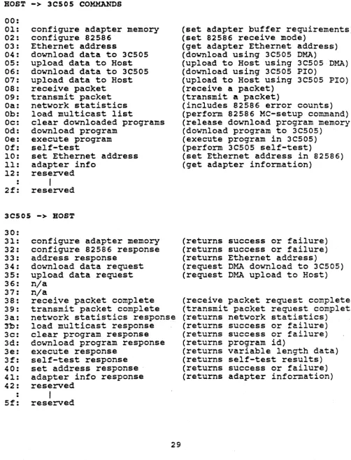
TABLE 1 : PCB COMMAND CODE SUMMARY HOST -> 3C505 COMMANDS
00:
01: configure adapter memory 02: configure 82586
03: Ethernet address
04: download data to 3C505 05: upload data to Host 06: download data to 3C505 07: upload data to Host 08: receive packet
09: transmit packet Oa: network statistics Ob: load multicast list
Oc: clear downloaded programs Od: download program
Oe: execute program Of: self-test
10: set Ethernet address 11: adapter info
12: reserved
:
I
2f: reserved
3CS05 -> HOST
configure adapter memory configure 82586 response address response
download data request upload data request n/a n/a 30: 31: 32: 33: 34: 35: 36: 37: 38: 39: 3a: 31:> : 3c: 3d: 3e: 3f: 40: 41: 42:
receive packet complete transmit packet complete network statistics response load multicast response clear program response download program response execute response
.
.
5f:
self-test response set address response . adapter info response reserved
I
reserved(set adapter buffer requirements) (set 82586 receive mode)
(get adapter Ethernet address) (download using 3C505 DMA)
(upload to Host using 3C505 DMA) (download using 3C505 PIO)
(upload to Host using 3C505 PIO) (receive a packet)
(transmit a packet)
(includes 82586 error counts) (perform 82586 MC-setup command) (release download program memory) (download program to 3C505)
(execute program in 3C505) (perform 3C505 self-test)
(set Ethernet address in 82586) (get adapter information)
(returns success or failure) (returns success or failure) (returns Ethernet address)
(request DMA download to 3C505) (request DMA upload to Host)
(receive packet request complete) (transmit packet request complete) (returns network statistics)
(returns success or failure) (returns success or failure) (returns program id)
[image:33.623.62.564.97.755.2]3.1.1 STATUS FLAG USAGE FOR PCB TRANSFER
The Adapter uses a 64-byte circular buffer to store the host byte stream sent through the Command Register. For protection against stray bytes (from Host aborted PCB transfers), the Adapter does not consider a PCB transfer complete until the Host status Flags (HSF2 and HSFl) go to state 11. Simultaneously, the TOTAL length of the PCB should be in the Command Register so the true beginning of PCB can be calculated. (This last total length is NOT included in the PCB data length field.) The Adapter uses its status flags (ASF2 and ASF1) similarly to signal "end of PCB" when sending a PCB to the Host.
The Adapter is always ready to read a PCB but it might not always be able to accept it. To indicate the acceptance of the PCB, the Adapter uses status flag-state 01 after the Host signals end-of-PCB. To indicate rejection, the Adapter uses status flag state 10. When the Adapter sends a PCB to the Host, it expects the Host to set its status flags similarly to signal acceptance or rejection.
In summary, the Adapter uses and expects the Host to use the following conventions:
Adapter or Bost Status Flaq SF2
o
o
11
SFl
o
1
o
1Undefined PCB accepted PCB rejected End of PCB
The state 11 is accompanied by the total length of the PCB just transmitted. After a PCB is received, the state 01 or 10 is used to signal acceptance or rejection of ·the PCB.
3.1.2 BOST TO ADAPTER REQUEST
- output the remainder of the PCB similarly, reducing the timeout period to SOOus. The Adapter remains in interrupt context to read PCB data.
- After the last actual PCB data byte is transferred, the Host must send one last byte signifying the TOTAL length of the PCB (excluding this byte). set the Host status flags to state 11 before writing the length.
- wait for adapter state 01 (accept) or 10 (reject). Assume a reject if a SOms timeout occurs.
3.1.3 ADAPTER TO HOST REQUEST OR RESPONSE
The 3C505 Adapter to PC Host request is made when the Adapter needs to read or write a block of host memory. The Adapter usually sends a response PCB after it has executed a host request.
The following method is used to transmit an adapter PCB to the Host:
- Load the PCB command byte into the Command Register; this interrupts the PC Host, synchronizing i t to the Adapter for the data transfer.
- Poll the Command Register Empty (ACRE) flag in the Adapter status Register. Abort the I/O if i t does not go empty within 20 ms.
- Output the remainder of the PCB similarly, timeout to SOous. The Host should remain context to read PCB data.
reducing the in interrupt
- After the last actual PCB data byte is transferred, the Adapter sends one last byte signifying the TOTAL length of the PCB. The Adapter status Flags are set to state 11 before writing the length.
3.2 PCB COMMANDS
3.2.1 HOS~ TO 3C505 PCB FORMATS
01H: Confiqure A~apter Memory. The Adapter allocates memory for the PCB command queue, receive command queue, multicast address list, 82586 frame descriptors, receive buffers, and download program data structures. Each PCB and receive command queue entry is large enough to buffer the maximum size PCB of 64 bytes. A multicast list is kept in adapter memory to be loaded into the 82586 LAN coprocessor when in multicast mode. Receive and transmit buffers of 1.6kb are alwp: is iJ.sei:' tQ decrease buff,~r
management and DMA overhead. The number of transmi~
buffers is fixed at one and is not confiqurable. If this command is not issued, the Adapter uses the default values shown in parentheses below. The Host should expect the adapter response PCB31H to confirm execution.
db db dw dw dw dw dw dw
01 OC ? ? ? ? ? ?
;command code
;length of data portion of PCB
;# command queue entries (10)
;# receive queue entries (20)
;# multicast addresses (0) ;# frame descriptors (20)
;*
receive buffers (20) ;# download programs (10)02H: Confiqure 82586. Instructs the Adapter to configure the 82586 LAN coprocessor into the given receive mode. If this configure command is not issued, the Adapter will use the default values shown in parentheses below. The Host should expect the adapter response PCB 32Hto confirm execution.
db 02 ;command code
db 02H ;length of data portion of PCB
dw ? ;receive mode
·
bit 2,1,0: receive mode (000),
000
=
station only 001=
plus broadcast03B: Ethernet Address. Requests Adapter to return the Ethernet address stored in its address PROM. The Adapter sends the PROM address in PCB 33H.
db db
03 00
:command code
;length of data portion of PCB
04H: Download Data To 3CSOS. Requests the Adapter to DMA download data through the data register. The direction bit must be set to the download direction before issuing the command. If the command is accepted, the Adapter sets up the DMA transfer and expects the Host to supply the required number of bytes. There is no Adapter response PCB for this command.
db 04 ;command code
db 06 ;length of data portion of PCB
dw ? ;data block byte length (must be even) dw ? ;Adapter destination offset
dw ?
·
,
"
"
segmentOSH: Upload Data To Host. Requests the Adapter to use its DMA channel to upload data through the data register. The direction bit must be set to the upload direction before issuing this command. If the command is accepted, the Adapter sets up the DMA and expects the Host to read the given number of bytes. There is no adapter response PCB for this command.
db 05 icommand code
db 06 ;length of data portion of PCB
dw ? idata block byte length (must be even) dw ? ;Adapter source offset
dw ?
·
,
"
It segment06H: Download Data To 3C50S. Operates as command code 04H, except that the Adapter uses programmed input/output (PIO) instead of DMA. The direction bit must be set to the download direction before issuing this command. There is no adapter response PCB for this command.
db 06 icommand code
db 06 ilength of data portion of PCB
dw ? ;data block byte length (must be even) dw ? ;Adapter destination offset
07H:
OSH:
Upload Data To Host. Operates as command code 05H, except that the Adapter uses PIO instead of DMA. The direction bit must be set to the upload direction before issuing this command. There is no adapter response PCB for this command.
db 07 icommand code
db 06 i length of d'ata portion of PCB
dw ? idata block byte length (must be even) dw ? iAdapter source offset
dw ? ; II II segment
Recei~;;i(~ P~,cket. Pequests 'the Adapte,r, to rece:l're " Ethernet packet. The packet type of interest is d~fined
previously by the Configure PCB 02H. _ When the receive is complete, the Adapter responds with PCB 3aH. The Host should set up to input the packet data and then accept the response. The Adapter will DMA upload the packet through the Data Register.
db db
dw dw dw dw
OS 08 ? ?
?
?
icommand code
;length of PCB data portion ;offset of Host receive buffer ;segment of Host receive buffer
iHost receive buffer length in bytes itimeout in 10ms increments (zero is
i no timeouti maximum is 32767 ticks) 09H: Transmit Packet. Requests the Adapter to transmit a packet. If the PCB is accepted, the Host should DMA download the packet data through the Data Register. When the transmit is complete, the Adapter responds with PCB 39H.
db
db
dw dw dw
09H 06 ? ? ?
;command code
ilength of PCB data portion ;offset of Host transmit buffer isegment of Host transmit buffer
OBB: Load Multicast List. The Adapter will add the given list of multicast addresses to the 82586 multicast list. A zero length list will cause the Adapter to clear all multicast addresses and multiple PCB's can be issued to create lists greater than ten entries. The maximum number of addresses in the PCB is ten. The response PCB 3BH will contain command completion status.
db db db db OBH 6*n
6 dupe?) 6 dupe?)
;command code
;length of PCB data portion ;Multicast address 1
;Multicast address n (10 maximum)
OCH: . Clear Downloaded- ProqramEi. This command releases all adapter memory previously allocated to downloaded progams. The adapter response PCB 3CH will contain the number of paragraphs of program memory available.
db
db
OCH
o
;command code ;length of PCB data portionODH: Download Proqram. Downloaded programs occupy adapter memory not used for packet buffers or system overhead. If this request is accepted, the Adapter will DMA download the program. When done, the Adapter responds with PCB 3DH containing a "program id". The Adapter always provides paragraph alignment to each downloaded program. It is suggested that the Adapter be hard reset before a Download Program sequence.
db db dw ODH 02 ?
icommand code
;length of PCB data portion ;program length in bytes
OEB: Execute Proqram. The Adapter will pass control to the program defined by the program ide The first executable code is assumed at offset zero relative to the beginning of the downloaded program. The calling sequence to the downloaded program is described in section 3.3.5, function 2. The Adapter, when done, responds with PCB 3EH.
db db dw db OEB 02+n ?
n dupe?)
;command code
ilength of PCB data portion ;program id
OFH: Sel~-Test. The Adapter will execute its self-test. Adapter, when done, responds with PCB 3FH.
db db
OFH
o
;command code ;length of PCB data portionThe
10H: set Ethernet Address. The Adapter will issue an lA-setup command to the 82586 coprocessor specifying an' Ethernet station address. If this command is not used, the address from the Adapter's Ethernet address PROM is used to configure the 82586.
lOH 6
6 dupe?)
;command code
;length of PCB data portion ;Ethernet address
11H: Adapter Info. Requests the 3C505 Adapter to send general information that describes the adapter configuration. The Adapter, when done, responds with PCB 41H.
db
db
llH
3.2.2 3C505 TO HOST PCB FORMATS
31H: Configure Adapter Response. After the Adapter has
32H:
33H:
34H:
3SH:
initialized the PCB command queue and the multicast address storage area, i t responds with status in this PCB. db db dw 3lH 02 ? ; command
;length of PCB data portion ; status 0
=
successfulConfigure 82586 Response. After the Adapter has initial-ized the 82586 coprocessor using parameters in the PCB 02H command, i t responds with status in this PCB.
db db dw 32H 02 ?
;command code
;length of PCB data portion istatus 0
=
successfulEthernet Address Response. The Adapter returns the 6-byte Ethernet address in this response PCB. The address has previously been read from the Ethernet address PROM and stored into memory.
db db db
33H 06
6 dupe?)
icommand code
;length of PCB data portion iEthernet address
Download Data To 3CS05. In this PCB, the Adapter requests that the Host download a block of host memory to the 3C505. If the command is accepted by the Host, the Adapter will use DMA to transfer the data through the data register.
db 34H icommand code
db 06 ilength of data portion of PCB
dw ? idata block byte length (must be even) dw ? iHost data block source offset
dw ? ;Host II segment
Upload Data To Host. In this PCB, the Adapter requests that the Host upload a block of data into Host memory. If the command is accepted, the Adapter will set up a D¥~ to transfer the appropriate data through the data register. db db dw dw dw 35H 06 ? ? ?
;command code
ilength of data portion of PCB
idata block byte length (must be even) ;Host data block destination offset
38H: Packet Received Response. When the Adapter receives a packet and there is an outstanding Host request to receive a packet, the Adapter sends this response PCB and follows i t with a DMA upload. The number of bytes DMA'ed will not exceed the buffer length specified in the receive packet command PCB 8Hi extra packet data is discarded.
39B: 3~: db db dw dw dw dw dw dw dd 38H 10H ? ? ? ? ? ? ?
Transmit Packet transmission is PCB.
db 39H
db 08H
dw ?
dw ?
dw ?
dw ?
icommand code
ilength of PCB data portion ;offset of Host receive buffer isegment of Host receive buffer inumber of bytes to be DMA'ed iactual packet length
icompletion status 0 = successful
i -1
=
timeouti82586 receive status
idouble word time tag in 15us ticks Complete. The status of a packet returned to the Host in this response
icommand code
ilength of PCB data portion ioffset of Host transmit buffer isegment of Host transmit buffer ;completion status 0 = successful :82586 transmit status
Network statistics Response. The Adapter returns the total packet counters and the 82586 error counters in this response PCB.
db db dd dd dw dw dw dw 3~' OCH ? ? ? ? ? ?
icommand code
;length of PCB data portion itotal receive packets
itotal transmit packets iCRC error counter
3CH: Clear Downloaded Program Response. To clear the down-loadable program memory, the Adapter reinitializes the structures and variables describing each downloaded program. The Adapter sends the amount of program memory available in paragraphs in this response PCB.
db db dw 3CH 02 ?
icommand code
ilength of PCB data portion ;amount of downloadable program ;memory in paragraphs
3DB: Download Program Response. A downloaded program is assigned a "program id" by the Adapter. The id is used by
the Host and Adapter when specifying which downloaded program to execute or has executed.
db db dw dw dw dw 3DH 08 ? ? ? ?
icommand code
;length of PCB data portion
;program id: > 0 , if allocated iprogram offset in adapter memory iprogram segment in adapter memory iremaining memory in paragraphs
3EH: Execute Program Response. After a downloaded program has executed, i t sends this response PCB to the Host. The return status and parameters are program dependent.
db db dw db 3EH 02+n ?
n dupe?)
iconunand code
;lenqth of PCB data portion
;program id: -1 if bad id in request ;return status and parameters
3FH: Self-Test Response. The adapter self-test consists of a ROM checksum, non-destructive RAM test, and internal loopback test on the 82586. status of the test is returned in this PCB.
db db dw dw 3FH 2+2n ?
n dupe?)
;command code
;length of PCB data portion ;self-test status
; and optional failure data
The self-test status codes and failure data for each are:
#
o
1 2 3 STATUS no errors ROM checksum RAM test 82586 testFAILURE DATA none
computed checksum value
failed memory offset:seqment status word:
40H: set Address Response. address in the 82586,
After the Adapter sets the Ethernet this response is sent to the Host.
db db
dw
40H 2 ?
icommand code
ilength of PCB data portion istatus O=successful
41H: Adapter Info Response. The Adapter formats a response containing the ROM revision code, ROM checksum value, total amount of memory in kilobytes, and the segment/ offset pointer to free memory.
db db
dw dw dw dw dw
41H 10 ? ? ? ? ?
icommand code
ilenqth of PCB data portiori
iROM revision level (Ox0300 = rev 3.0) ichecksum value in rom
iamount of memory in kbyte ifree memory offset
3.3 SYSTEM ROM UTILITIES
Programs downloaded into the 3C505 Adapter can access the adapter resources directly or through a set of utilities available in ROM code. To simplify and standardize usage, a set of soft interrupt vectors have been allocated to support the following:
*
Host I/O*
Network I/O*
Configuration/status*
System Timer*
Download Program Support*
PCB Command Processing*
Receive Packet Processing*
Timed execution*
PCB EnqueuingThese vectors may be replaced or chained to by user downloaded programs. To chain to a vector, the downloaded program should first save the current vector before replacing i t with a pointer to itself. A program then gains control when the vector is invoked. As appropriate, the program should pass control to the next program in the chain.
The 3C505 ROM utilities always save and restore the calling program's SS, DS, ES and SP. It is suggested that downloaded programs also maintain these registers.
3.3.1 HOST I/O SUPPORT: INT aOH
This group of function allows upload and download of data and command blocks between the Adapter and PC Host. Both DMA and PIO methods of IO are supported.
01H: Download Request. The Adapter formats a download for Host If the should request PCB, sends i t to the Host, and waits
acknowledgement (HSF2 and HSF1 state 01 or 10). Host accepts the request (state 01)1 the caller proceed with the data transfer.
ax ~ 1
es:bx cx
dx
function code
Host source buffer address
buffer length bytes (must be even; maximum 64kb) initial timeout in 10ms increments
(maximum is 32767 ticks) Return: carry clear if successful
02H: DMA Upload Request. The Adapter formats a upload request PCB and sends i t to the Host. If the request is acknowledged by the Host (HSF2 and HSFl state 01), the Adapter should perform the data transfer.
ax
=
2 es:bx cx dxfunction code
Host destination buffer address
buffer length bytes (must be even: maximum 64kb) initial timeout in 10ms increments
(maximum is 32767 ticks) Return: carry clear if successful
'Try set if error, ax
=
errCJt' code03B: Get Primary Command Block From Host. This function reads a PCB through the Command Register and stores i t into the destination buffer.
ax = 3 function code es:bx buffer address
cx buffer length bytes
dx initial timeout in 10ms increments (maximum is 32767 ticks)
Return: carry clear if successful
carry set if error, ax
=
error code04H: Send primary Command Block To Host. This function sends the given PCB buffer to the Host and waits for host acknowledgement either accept or reject.
ax
=
4 function code es:bx buffer addresscx total buffer length bytes
dx initial timeout in 10ms increments (maximum is 32767 ticks)
Return: carry clear if successful and accepted carry set if error, ax = error code
ax - 5 ax -= 6 es:bx ex dx
DMA download or
PIO download buffer address
buffer length in bytes to transfer (must be even) timeout in lOms increments
(maximum is 32767 ticks) Return: carry clear if successful
carry set if error, ax -= error code
07H: OSH: Host Data output. Assuming that the Host is already configured to perform an upload, this function transfers adapter data (using DMA or PIO) from the adapter buffer to the Host. The comments descriping DMA in int SOH function OSH also apply here.
ax -= 7 ax -= S es:bx ex
dx
DMA upload or
PIO upload buffer address
buffer length in bytes to transfer (must be even) initial timeout in lOms increments
(maximum is 32767 ticks) Return: carry clear if successful
carry set if error, ax - error code
09H: OAB: Accept or Reject PCB. When a PCB is read using int SOH function 3, the protocol described in section 3.1.1 requires that the PCB be accepted or rejected. The following function codes provide this ability to downloaded programs:
ax
=
09H Accept Host PCB ax=
OAR Reject Host PCBFunction 9 to accept a PCB also includes a Data Register flush operation to prepare for a DMA or PIO data transfer.
OBH: Check DMA Complete. When a DMA transfer has been initiated, this function can be ~alled to check if the DMA has completed.
ax
=
OBH Check DMA Completedx timeout in lOms ticks (maximum is 32767 ticks) Return: carry clear if DMA done