Molecular Adsorption at the
Solid/Liquid Interface
Thesis submitted in accordance with the requirements of the
University of Liverpool for the degree of Doctor in Philosophy
by
Andrew Francis Bowfield
Department of Physics
If the facts don’t fit the theory, change the facts
solid/liquid interface. The variation in adsorption kinetics are studied as a function of concentration, pH, applied electrode potential and surrounding environment by the surface sensitive analytical techniques of Reflection Anisotropy Spectroscopy and X-ray Photoelectron Spectroscopy.
An electrochemical investigation into the surface reconstructions of Au(110) and their associated RA profiles is undertaken. The spectral profiles of Au(110) in 0.1 M H2SO4/Na2SO4, NaClO4/HClO4 and NaClO4 electrolytes were observed as a function of potential and spectral signatures of the different reconstructions are assigned.
The adsorption of adenine and its monophosphate (AMP) on Au(110) was studied using RAS. It is shown that both molecules adsorb in a vertical orientation through sites common to the base through formation of base stacked layers. Application of a phenomenological Lorentzian transition model and rotations about the polarisation direction of the incident light suggest that the molecules align along the [11 0] principal axis of the substrate. Linear simulations show that the orientation of adenine at sub-saturation coverage is the same as that when a monolayer is adsorbed and that adenine does not adsorb on the surface at sufficiently alkaline pH.
The attachment of thiolated ss-DNA on a functionalised diamond surface and the subsequent detection of hybridisation are discussed. High resolution XPS spectra are used to characterise both the integrity and structure of the organic thin film and its modification to precipitate DNA adsorption.
Acknowledgements
I would firstly like to thank Professor Peter Weightman for providing me with the opportunity to be a part of his research group. His wit, generosity, knowledge and endless enthusiasm will forever accompany me. Not just a good scientist, a good man. Of course, I would never have gotten this far without Caroline ‘time for tea’ Smith and her invaluable help and advice. I would also like to thank Trevor Farrell and Paul Harrison whose technical expertise is second to none. Indeed, Paul Unsworth deserves a mention for all the guidance he has shown on the ever dependable XPS kit. Thanks also go to fellow PhD students Gerard Dolan, Nick Almond, Gareth Holder and James Convery. To Chelo Cuqeurella and Amy Schofield also thanks.
On a personal note, it is often close friends who amplify what an enjoyably tough PhD is really about. The following people have not only encouraged me to consume far too much alcohol, but also discuss life, the universe and physicists over many lost hours: Michael ‘two socks’ Cormack, Alex Brownrigg, Dan Poulter, Abdi Noor, Craig Wiglesworth, Joe Parle, Chris Mansley, Joe Croft, Craig Gray-Jones, Alex Grint, David Scraggs and Richard Miller. And not forgetting the girls Ella Morley, Katherine Elliott and Pauline Gallon.
A very special thank you must be extended to an extraordinary person who has accompanied me throughout these last four long years; Nina Morley. Love, laughter and support have always been in endless supply when submission seemed so far away. My gratitude to her is boundless. Her embracing approach to life is truly unique.
Atomic force microscopy: AFM Chemical vapour deposition: CVD
Circular dichroism: CD
Complete active space with second-order perturbation theory: CASPT2 Complete neglect of differential overlap: CNDO
Configuration interaction perturbing a multi-configurational zeroth-order wave function selected iteratively: CIPSI
Cyclic voltammetry: CV
Cytidine 5'-monophosphate: CMP
Decanethiol: DCNT
Deoxyribonucleic acid: DNA
Intermediate neglect of differential overlap/screened approximation: INDO/S
Linear dichroism: LD
Low energy electron diffraction: LEED Low energy helium atom diffraction: LEAD
Photoelastic modulator: PEM
Photomultiplier tube: PMT
Scanning tunnelling microscopy: STM
Self-assembled monolayer: SAM
Spectroscopic ellipsometry: SE Saturated calomel electrode: SCE Surface enhanced raman spectroscopy: SERS Time dependant density functional theory: TDDFT
Ultra high vacuum: UHV
X-ray diffraction: XRD
Abstract ... i
Acknowledgements... ii
Acronyms ... iii
Chapter 1:
Introduction...1
1.1: Emergence of Interdisciplinary Approaches... 2
1.2: Surface Science and the Solid/Liquid Interface ... 3
1.3: Importance of Electrochemistry... 4
1.4: Thesis Aims... 4
1.5: Thesis Structure... 5
1.6: References ... 7
Chapter 2:
Experimental Techniques and Components... 8
2.1: Reflection Anisotropy Spectroscopy... 9
2.1.1: The RA Spectrometer and its Optical and Electronic Components... 11
2.2: The Propagation of Light Through the System... 16
2.2.1: The Jones Matrix Formalism ... 21
2.2.2: Errors ... 28
2.3: Electrochemistry ... 29
2.3.1: Measuring Electrode Potentials... 32
2.3.2: The Electrochemical Cell ... 33
2.3.3: Cyclic Voltammetry... 34
2.4: X-ray Photoelectron Spectroscopy... 36
2.4.1: The VSW ESCA Instrument ... 40
2.4.2: Monochromated X-ray Source... 41
2.5: References ... 44
Chapter 3:
The Au(110) Surface... 46
3.1: Introduction... 47
3.2: Surface Phase Transitions... 47
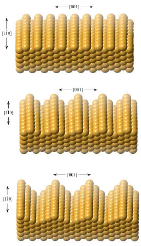
3.3: Physical Structure of the Au(110) Surface... 48
3.3.1: Au(110) in UHV... 49
3.3.2: Electrochemistry of Au(110) ... 53
3.4: Electronic Structure of Au(110)... 55
3.5: RAS of Au(110): Origin of Spectral Features ... 57
3.6: The Three-Phase Model... 62
3.6.1: The Dielectric Function ... 63
3.6.2: The Lorentzian Transition Model... 64
3.7: Crystal Preparation... 66
3.8: Simulations Using the Three-Phase Model ... 67
3.9: Spectral Signatures of the Different Reconstructions of Au(110): An Electrochemical Investigation ... 68
3.9.1: Au(110) in 0.1 M H2SO4/Na2SO4 at pH 1.36 ... 69
3.9.2: Au(110) in 0.1 M NaClO4/HClO4 at pH 1.18 ... 82
3.9.3: Au(110) in 0.1 M NaClO4 at pH 6.14... 88
3.10: Comparison of the (1x1), (1x2) and (1x3) Reconstructions in Different Electrolytes and Varying pH. ... 98
3.11: Simulation of (1x2)... 102
3.12: Summary... 104
3.13: References ... 105
Chapter 4:
Determination of the Structure of Adenine Monolayers
Adsorbed at Au(110)/electrolyte Interfaces ... 110
4.4: Electronic Spectrum of Adenine ... 124
4.5: Simulation of Au & Au + Adenine RA spectra... 130
4.6: Simulation of Sub-Saturation Adenine Spectrum... 141
4.7: The Effect of Electrode Potential on Adenine Adsorption ... 142
4.8: Effect of pH Variation in the Supporting Electrolyte ... 148
4.9: Summary... 151
4.10: References ... 152
Chapter 5:
RAS of Alkanethiol Adsorption at Au(110)/liquid
Interfaces ... 157
5.1: Introduction... 158
5.2: Experimental Procedure ... 160
5.3: The Orientation of DCNT as a Function of Coverage... 162
5.4: Azimuth Dependent RAS as a Function of Surrounding Environment... 168
5.5: Summary... 173
5.6: References ... 174
Chapter 6:
Detection of DNA Hybridisation on a Functionalised
Diamond Surface ... 177
6.1: Introduction... 178
6.2: Experimental Procedure... 180
6.3: XPS of Amine Functionalised TFAAD Protected Diamond... 184
6.4: Determination of Elemental Ratios:... 190
6.5: Structure of the Monolayer Films... 191
6.6: XPS of Amine Terminated Deprotected Diamond... 194
6.8: Detection of DNA Hybridisation ... 201
6.9: Summary... 202
6.10: References ... 202
Chapter 7:
Conclusions ...205
7.1: Summary of Findings ... 206
7.1.1: The Au(110) Surface ... 206
7.1.2: Adenine... 206
7.1.3: Decanethiol ... 207
7.1.4: DNA on Diamond... 208
7.2: Future work... 209
Appendix ... 211
A.1: XPS of Amine Terminated Deprotected Diamond (II) ... 212
Chapter 1: Introduction
1.1: Emergence of Interdisciplinary Approaches
"Now I am become Death, the destroyer of worlds" J. Robert Oppenheimer famously quoted as he witnessed the first detonation of an atomic bomb at the Manhattan Project headquarters at Los Alamos National Laboratory in New Mexico thereby capturing in a rather astonishingly morbid statement the impact of the physical sciences on the twentieth century. Of course, this is not to suggest that this was the only impact
of a post relativity science community on the wider world, although it was without doubt the most noticeable. After Einstein had revolutionised physics thinking with his famous ruminations on mass-energy equivalence in 1905, the natural sciences became questions of the minute and how they impacted the large and visible world which humans inhabit. Advances in quantum mechanics, harnessing nuclear fission as a platform for safe, effective electricity generation and the immunisation programmes which rendered many diseases all but extinct gave us a far deeper understanding of not just our world but the universe as a whole. The latter half of the previous century bore witness to the semiconductor revolution which heralded the age of the computer microchip and altered the course of human history irrevocably. The problem with most of these discoveries is that their full ramifications were often only felt in solitary scientific communities. The first years of the twenty-first century confined this approach to science research to the dustbin.
One such area where physical approaches can be applied to biological systems is the interaction and adsorption kinetics of molecules at surfaces. This field is already well established [1] with an array of techniques available with which to study various properties [2]. It is only in a truly interdisciplinary and collaborative approach to science that solutions to many of mans immediate ailments lie.
1.2: Surface Science and the Solid/Liquid Interface
Surface science has developed at a fast pace since its inception over forty years ago. The ability to maintain UHV has allowed techniques such as LEED, XPS and STM, which exploit the short mean free path of electrons and require contaminants from air to be kept at a minimum, to flourish with abandon and have become essential surface sensitive diagnostic tools. While these approaches are still important they cannot be applied to a solid/liquid interface, for example STM being susceptible to surface tip effects, and since there is an increasing need to study biological molecules in situ so as
to appropriately re-create an environment in which biological activity and functionality remains at a maximum, there is also a need for more versatile techniques. Hence understanding of the solid/liquid interface is a critical area of study for many scientists, however cataloguing the interactions occurring at this boundary is made difficult, rather ironically, by the presence of a supporting electrolyte or liquid.
The requirement to study biological systems in situ has led to the development
1.3: Importance of Electrochemistry
Electrochemistry is increasingly pivotal to the study of interfacial systems and coupled with the development of optical probes has applications in both scientific and industrial sectors [3,5,6]. Recently, it has been shown that the change in optical response of metal surfaces and molecular and chemical adsorbates can provide a wealth of information which can be used to further the understanding of these systems [5]. The interface between electrode surface and electrolyte is crucially important since it provides the site of the majority of interactions which have scientific and industrial applications. These include the development of DNA labelled nanoparticles, bioarray technology and the exploitation of surface plasmon resonance and heterogeneous catalysis [6]. Other electrochemical techniques such as CV do not provide enough surface structural information alone to gain a full understanding of the interface.
1.4: Thesis Aims
1.5: Thesis Structure
Chapter 2 Instrumentation and Theory
RAS is introduced and the experimental components described in detail. The layout of the spectrometer and a theoretical treatment of the passage of light through the system are considered. The current model of the solid/liquid interface at electrode surfaces is discussed along with how electrochemical control is maintained in the electrochemical cell. Also included is an introduction to cyclic voltammetry and its importance in investigating interfacial behaviours.
A detailed description of the X-ray photoelectron spectrometer employed is also included. The principles underpinning the technique, its components and an explanation of a typical XPS spectrum, including where the background signal originates, are detailed.
Chapter 3 The Au(110) Surface
The structure of the Au(110) surface is known to be sensitive to the environment in which it is studied and this section gives an overview of the physical configuration and previous RAS of the surface in both UHV and electrolyte in order to provide a basis upon which surface atomic arrangement can be explained. A Lorentzian transition model is described in an attempt to understand the changes in spectral profiles induced by molecular adsorption.
Chapter 4 The Adsorption of Adenine at the Au(110)/electrolyte Interface The orientation of biologically important molecules such as nucleic acid bases once adsorbed at an interface is important in the production of bio-electronics. The three-dimensional structure of adsorbed adenine on Au(110) is determined using rotations of the crystal through a plane perpendicular to the incident light in conjunction with a Lorentzian transition model and studied as a function of surface coverage, potential and pH.
Chapter 5 Alkanethiol Adsorption at Au(110)/liquid Interfaces
The gold/sulphur bond is known to be very strong and thiolated species with a hydrophobic backbone should self-assemble in such a fashion so as to try and exclude hydrogen bonding between separate molecules. The formation of a SAM is investigated as a function of coverage along with changes to the surrounding environment to determine variations in the back-bone orientation.
Chapter 6 DNA Hybridisation on a Functionalised Diamond Surface
RAS is shown to be sensitive to the hybridisation of single stranded DNA on an amine functionalised diamond surface. XPS data is fitted to highlight the removal of a protecting group originally attached to the amine and also to prove functionalisation has occurred in an ordered fashion across the surface.
Appendix
1.6: References
[1] Surface Science: The First Thirty Years, Surf. Sci. 299 – 300, 1-1054 (1994) [2] Introduction to Surface Physics, M. Prutton (Oxford University Press, 1998)
[3] P. Weightman, G. J. Dolan, C. I. Smith, M. C. Cuquerella, N. J. Almond, T. Farrell, D. G. Fernig, C. Edwards and D. S. Martin, Phys. Rev. Lett. 96, 086102 (2006)
[4] C. I. Smith, A. Bowfield, G. J. Dolan, M. C. Cuquerella, C. P. Mansley, D. G. Fernig, C. Edwards and P. Weightman, J. Chem. Phys.130, 044702 (2009)
[5] R. LeParc, C. I. Smith, M. C. Cuquerella, R. L. Williams, D. G. Fernig, C. Edwards, D. S. Martin and P. Weightman, Langmuir 22,3413 (2006)
Chapter 2: Experimental
Techniques and Components
2.1: Reflection Anisotropy Spectroscopy
Reflection anisotropy spectroscopy is a non-destructive optical probe developed from SE [1,2] which can be used to investigate surface structure by exploiting the anisotropy found at some of the surfaces of cubic crystals. Optical probes are generally strongly influenced by the optical response of the bulk specimen due to light penetration many atomic layers into the material. This lack of sensitivity is not shared by certain techniques such as XPS and LEED, conducted in UHV environments, which exploit the low mean free path of electrons to obtain surface sensitivity. A comparison between the electron escape depth vs light penetration into a solid is shown in Figure 2.1 and it is immediately clear that contributions from bulk layers would dominate the optical response of the system thereby preventing surface sensitivity.
[image:21.612.172.484.471.679.2]Crystalline materials such as gold have a cubic cell structure in which each atom in the material can be considered to occupy a position either at the corner of a cube or at the centre of each face of the cube (Figure 2.2). If one considers an infinite arrangement of these cubes, as is the situation when engaged in experimentation, the optical response of the bulk material at near normal incidence will be symmetrical in all
Figure 2.2: Examples of the three main cubic cell structures: primitive (left), body-centred
cubic (BCC, centre) and face-centred cubic (FCC, right).
directions (isotropic) as all planes of atoms will contribute to the signal equally. As a consequence, any reflections dominated by a particular plane/crystal axis (anisotropic) will arise solely from the surface. RAS is therefore able to provide a characteristic diagnosis of the surface electronic structure with the added benefit of versatility in the range of environments in which experiments can be conducted. Since these environments must consist of optically transparent media, an application to electrode surfaces in electrochemical surroundings becomes possible. RAS is therefore a useful addition to a somewhat limited group of techniques with the ability to function in these electrochemical conditions.
RAS is able to achieve surface sensitivity by measuring the difference in reflectance (∆r) of normal incidence linearly-polarised light between two orthogonal
directions in the surface plane (rx,ry) normalised to the mean reflectance (r) [Figure 2.3]:
(
)
y x
y x
r
r
r
r
r
r
+
−
=
∆
2
2.1.1: The RA Spectrometer and its Optical and Electronic
Components
RAS uses a similar experimental set-up to SE but with some significant differences. SE illuminates the sample with linearly polarised light near to the Brewster angle [4] whereas RAS illuminates the sample with linearly polarised light at near normal incidence (≤ 5˚). Originally labelled reflection difference spectroscopy (RDS), the technique was initially created by the need for a real-time monitor of III-IV semi-conductor growth at near atmospheric pressure [5]. Developed in the 1980s by Aspnes and co-workers [6], RAS has recently been applied to the study of metal surfaces in UHV and air [7], the metal/liquid interface in the electrochemical environment [8] and the adsorption of biological molecules onto electrode surfaces [9-13]. The individual components of the spectrometer are displayed in Figure 2.3. Each of the components is described in the order in which light passes through the system. Mirrors, not pictured in the schematic, are placed before and after the polariser and analyser to facilitate the position of the focal length of the light. The axes of the gold substrate are defined as: [11 0] = rx and [001] = ry.
Xenon Lamp
A 75 Watt Super-Quiet 9 short arc xenon discharge lamp (Hamamatsu), in conjunction with a stabilised power source (Hamamatsu C4621-02) which minimises fluctuations from the mains supply by removing spikes, provides a high intensity point source of light. The lamp functions by means of an arc discharge when high voltages are applied across the anode to a high performance cathode in a xenon gas environment. Such a light source is desirable for RAS studies due its reliable and stable output of a continuous spectrum in the infrared to ultraviolet range (1.5 – 5.5 eV). Owing to the fact that xenon gas pressure in the lamp varies for up to 1 hour after power up and does not reach thermal equilibrium and thus a maximal radiant intensity until after this point, care must be taken to only begin experimentation at least 1 hour after the lamp is switched on so as to ensure an unchanging photonic flux can be obtained with confidence.
Mirrors
Concave mirrors are employed to produce a parallel beam of focused light from the incident diverging light emitted by the Xe-lamp and, utilising the intrinsic astigmatism of the mirrors, to re-focus the light reflected from the sample surface onto the monochromator entry slit after it has passed through the photo-elastic modulator and analyser. The input of the monochromator is a narrow vertical slit; it is therefore possible to use the tangential focus as the image at the input slit and so reduce any sagittal component from the analyser. These mirrors are front coated aluminium on glass, with a thin silica coating to prevent mechanical abrasion.
Polariser
consist of two attached quartz prisms that separate the ordinary and extraordinary polarised beams which are polarised perpendicular to each other. Glan prism polarisers separate the two polarised beams by total internal reflection and consequently a single beam emerges. A single beam is often preferable when used with UHV apparatus since they pose no restrictions on geometry to avoid the 2nd beam thereby allowing a more compact experimental layout. The RAS instrument detailed in this thesis makes use of Rochon type prisms due to a more efficient transmission of light in the UV region. This is a reasonable choice since UHV RAS measurements are not conducted in this body of work. Nevertheless, care must be taken to ensure the two beams which exit the polariser do not overlap.
Low-Strain window
After the light has been polarised, it next encounters a low-strain silica window prior to entering the electrochemical cell. This window itself will make a small contribution to the detected RAS signal as it will inherently possess some inhomogeneous birefringence. This contribution can be removed by subtracting a correction spectrum from all raw experimental data.
Photoelastic Modulator
The PEM (Hinds Instruments Inc., PEM90 Quartz) is crucial to how RAS is able to attain surface specificity and is displayed in Figure 2.4. Sir David Brewster discovered in 1816 that applying a mechanical stress to a normally transparent isotropic substance could induce an optical anisotropy in that same material. In some materials, namely fused silica in this instance, this mechanical effect manifests itself in the form of a stress-induced birefringence (photoelasticity).
The PEM is in effect a tuneable wave-plate which modulates the polarisation ellipse of the light reflected from the surface by exploiting the aforementioned process. This is to ensure collection of both real and imaginary elements of the light wave by driving a quartz piezoelectric transducer at 50 kHz, which is the natural resonant frequency of the coupled fused silica optical element. One can effectively consider the incident ellipse as having two orthonormal components polarised parallel and perpendicular to the modulation axis of the PEM. The PEM introduces an oscillating birefringence into the centre of the optical element and acts solely on the parallel component thus, as the silica is compressed the component polarised parallel to the axis of modulation travels faster than the perpendicular component and vice-a-versa when the optical element is stretched. The phase difference between the components at any instant is called the retardation (Γ) where the peak retardation is defined as the amplitude of the sinusoidal retardation as a function of time. Consequently, as elliptically polarised light impinges, the PEM introduces a phase modulation dependent upon the polarisation state.
Analyser
Monochromator
To enable a spectroscopic analysis of the reflected light, it is necessary to split the light into its constituent wavelengths. A Jobin Yvon monochromator (H10), consisting of a holographic grating with 1200 grooves mm-1, with a spectral range of 1.5 - 6.2 eV (200 to 800 nm) is utilised to this end. The position of the grating and hence the wavelength of light entering the detector is determined using a computer controlled stepper motor.
Detection
Located immediately behind the exit slit of the monochromator is a Hamamatsu multi-alkali cathode photomultiplier tube (PMT Hamamatsu R955). The PMT measures the intensity of the light and converts the intensity-modulated waveform into a current. This current is often minute (of the order of nA) and is therefore in need of amplification. The amplified signal is then converted to a potential relative to the initial intensity of the incoming light. The signal consists of an AC component, related to the surface anisotropy, superimposed on a DC offset, which is related to the reflectivity. These two components then need to be analysed separately which requires the use of a lock-in amplifier.
Silicon photodiodes are another type of detector which can also be used in RAS set-ups which are optimised for longer wavelength detection (200 - 1100 nm). The spectral range over which these types of detectors function does not extend into UV, however detection in this region can be attained through the application of an appropriately chosen coating which converts UV photons for detection within the visible range. This process ultimately results in a loss of sensitivity in the visible range and to avoid this occurrence a PMT was chosen for this instrument.
Lock-in Amplifier
Fourier coefficients of the first and second harmonics of the signal which carries the real and imaginary parts of the RA response respectively. Since such instruments are able to detect signals at very specific frequencies that would otherwise be obscured by noise, they are critical to the successful detection of the RA signal.
So as to produce accurate measurements and correct identification of the signal of interest, the lock-in is supplied with a reference voltage of the same frequency and phase relationship as that of the signal. Any differences between the frequencies of the signal of interest compared to this locked in signal will then be tracked. In this case the locked in reference signal is taken from the PEM.
2.2: The Propagation of Light Through the System
Thus far, only the optical considerations and signal analysis components of the spectrometer have been discussed. This section describes the theoretical applications to RAS in a quantitative manner using a highly successful mathematical formalism.
The accurate measurement of a RA signal requires a comprehensive method of determining the state of polarisation of the light reflected from the surface. It is pertinent to initially define the electric field vector, E, of a light wave which can be
represented as a superposition of two orthogonal states.
)
,
(
)
,
(
)
,
(
z
t
E
z
t
E
z
t
E
=
x+
ywhere
)
cos(
)
,
(
0x xx
z
t
E
kz
t
E
=
−
ω
+
φ
and
)
cos(
)
,
(
0y yy
z
t
E
kz
t
E
=
−
ω
+
φ
)
t
kz
cos(
yˆ
)
t
kz
cos(
xˆ
)
t
,
z
(
=
E
0x−
ω
+
E
0y−
ω
+
δ
Ε
where δ = φy– φx and is the relative phase between the two components. The direction of polarisation of the resultant wave depends on both its relative projection along each axis and δ. When δ = mπ for m = 0, ±1, ±2, ±3,… the wave is confined to a solitary plane and is said to be linearly polarised. If either E0y or E0x = 0, the wave is limited to vibrations along the x or y axes respectively. For non-zero magnitudes of both
components, the linearly polarised light is inclined at an angle α to the x axis defined as
[Figure 2.5]: = − y x E E 0 0 1 tan α
The polarisation of the resultant wave will be restricted to the positive x axis if
δ = 0 whereas if the phase difference is ± π, polarisation will lie along the negative x
axis. If a phase lag of an integer multiple of ± π/2 exists between the two components but they possess equal magnitudes (E0x = E0y), a state of circular polarisation is achieved. In this polarisation state the magnitude remains constant as the wave propagates through space, but the direction of E fluctuates with time following a
circular path with angular frequency ω. If the resultant vector not only rotates in this fashion but is also accompanied by variations in magnitude, the result is a state of elliptical polarisation. Elliptical polarisation occurs when either E0x ≠ E0y and δ is a multiple of ± π/2 or when E0x = E0y but δ is an arbitrary angle.
Figure 2.5: Linear polarisation states determined from the magnitudes and phases of E0x and
E0y [15].
analyser. As this action is only impacted upon elliptically polarised light, it is possible to extract harmonics from the amplitude modulation giving information deriving exclusively from the surface anisotropy. Circularly polarised light originating from the bulk response will pass through the modulator unaffected as the intensity of the resultant vector is the same in all phases.
Figure 2.6: Circular polarisation states [15].
Figure 2.7: Elliptically polarised light. Left: Phase difference of ±
2
π and E0x ≠ E0y. Right:
E0x = E0y and phase difference not equal to ±
2
As Jones Calculus is applicable in this instance the resulting wave, E, can now be
described much more concisely as:
=
δ δ y i y x i xe
E
e
E
0 0t)
(z,
E
The implementation of the Jones vector (M) allows the polarisation state of the light,
from its initial polarisation (Ei) emerging from the polariser to its final polarisation (Ef) arriving at the detector, to be determined as the light traverses the RAS instrument due to its ability to fully detail the effect on the light of the optical components.
i f
ME
E
=
(2.1)The Jones matrix M is formed by combining in sequence the 2 x 2 matrices which
describe the effect that each of the optical components has on the polarisation state of the light. Each component has its own set of optical axes - the polariser and analyser have transmission (t) and extinction (e) axes while the PEM has fast (f) and slow (s)
axes. The axes of the sample (x,y) are taken to be in the [11 0] and [001] surface directions and define the reference frame for each component thus rotation matrices, labelled R, are used to convert the Jones vector representing the polarisation state of
the light to those of the optical component with which it is interacting.
( )
( )
( )
( )
( )
θ
θ
θ
−
θ
=
cos
sin
sin
cos
θ
R
Figure 2.8: The orientation of the reference frames for each optical component relative to the
xy frame. All angles are positive in the anticlockwise direction [14].
axis of the modulator. P, M and A are referenced to the x direction of the sample and
are characterised as positive for an anti-clockwise rotation.
2.2.1: The Jones Matrix Formalism
Light emerging from the xenon lamp is unpolarised so it cannot be assigned an appropriate Jones matrix. However, after passing through the polariser it is in a definable polarisation state for the remainder of its journey through the instrument. Once through the polariser, it can be assigned the Jones matrix te
P
T , since it is in the te
reference frame of that component.
=
0
0
0
1
te P
T
Next, to ensure the light is in the xy plane of the sample, TPtemust be multiplied by the
−
=
−
=
0
sin
0
cos
0
0
0
1
cos
sin
sin
cos
P
P
P
P
P
P
R(P)T
Pte (2.2)Before reflecting from the surface, the light will encounter a strain-free window as it enters the electrochemical cell. The orientation of the window axes are unknown and as such are assumed to be commensurate with those of the xy frame of the sample. It is
likely the window will contain some birefringence (fast and slow axes) and hence some retardation of the incident light beam will occur. The effect of this action can be captured by:
=
WI i xy WIe
T
δ0
0
1
(2.3)where, δWI is the retardation of the incident beam by the window. δ is defined as:
(
n
en
o)
d
4
−
=
λ
π
δ
(2.4)where, d is the thickness of the material, λ is the wavelength of the light, and ne, no, are the refractive indices of the extraordinary and ordinary directions of the material respectively. The light then impinges upon the surface and after reflection will pass through the window as it exits the cell. The light will leave via a different part of the window with an associated retardation δWO. The Jones matrix for the surface is:
After exiting the cell, the light meets the PEM. To change the lights’ reference frame from that of the surface to that of the PEM, the rotation matrix must once again be utilised:
(
) (
)
−
=
−
=
δ δ δM
cos
e
M
sin
e
M
sin
M
cos
M
cos
M
sin
M
sin
M
cos
e
i M i M i M0
0
1
R(M)
T
Sfs(2.6)
The analyser then converts the light from phase-modulated to an amplitude-modulated signal, requiring the same matrix as that applied for the polariser and the rotation matrix.
(
)
−
−
−
=
−
−
−
−
−
=
−
0
0
)
sin(
)
cos(
)
cos(
)
sin(
)
sin(
)
cos(
0
0
0
1
M
A
M
A
M
A
M
A
M
A
M
A
M
A
R
T
Ate(2.7)
The complete matrix representing the final polarisation state of the fully propagated light, M, is obtained by combining the matrices of each element. Matrices are
non-commutative and as such the matrix for each component must operate in the order in which the light interacts with them. Combining Equations (2.2), (2.3), (2.5), (2.6) and (2.7) in order, the Jones matrix for the system becomes:
te P xy WI xy S xy WO fs M te
A
R
A
M
T
R
M
T
T
T
R
P
T
T
M
=
(
−
)
(
)
(
)
=
0
0
0
11a
M
where: ) P sin e e r ))( M cos e )( M A sin( M sin ) M A cos( ( ) P cos r ))( M sin e )( M A sin( M cos ) M A (cos( WI WO M M i i y i x i δ δ δ δ − − − − − − − − = 11 a (2.8)The values of the angles P, A and M used are -45°, 0°, and 45° respectively [Figure 2.8]. Thus:
,
2
1
)
45
sin(
±
°
=
±
,
2
1
)
45
cos(
±
°
=
sin(
0
°
)
=
0
,
cos(
0
°
)
=
1
Putting the above values into Equation (2.8) gives:
)
e
(
e
e
r
)
e
(
r
WO WI MM i i i y i x
1
2
2
1
2
2
a
11=
+
+
δ−
δ δ δ
(2.9)
As a11 is the solitary non-zero term in the total system matrix, M, Equation (2.1) now becomes
=
=
0
0
1
0
0
0
11 11a
a
E
f (2.10)The window terms can also be simplified:
W WI
WO WI
WO i i i
i
e
e
e
It is possible to expand the exponential in terms of a power series since the total retardation induced by the low-strain window, although finite, is small:
(
)
W W W W ii
i
i
i
e
δW=
+
δ
+
δ
+
δ
+
...
≈
1
+
δ
!
3
!
2
)
(
1
3 2Using the above simplifications, Equation (2.9) is now:
)]
1
(
)
(
)
[(
2
2
1
11 M M i y W i y x yx
r
r
r
e
i
r
e
r
a
=
−
+
−
δ−
δ
−
δ (2.11)rx and ry in Equation (2.11) represent the complex Fresnel reflection coefficients and can therefore be written in terms of their real and imaginary components:
,
ib
a
r
x=
+
r
y=
c
+
id
De Moivre’s theorem can be applied to express the term relating to the retardation of the modulator as:
)
sin(
)
cos(
M Mi
i
e
δM=
δ
+
δ
After some trivial manipulation a11 becomes:
( )
2
2
a
11=
α
+
i
β
(2.12)where α and β constitute the real and imaginary parts of a11. If one assumes that the
analyser is no longer transformed and the detector would only measure the time dependent intensity at each wavelength. The measured intensity, I, is proportional to
the square of Ef, which is dependent upon a11, thus:
( )
2 2 211
2
2
=
α
+
β
∝
a
I
After some extensive algebraic manipulation, this becomes:
(
) (
) (
)
[
]
(
) (
) (
)
[
]
( )
(
) (
)
[
W]
( )
MM W W
bd
ac
dc
ad
d
c
d
c
b
a
d
c
d
c
b
a
a
I
δ
δ
δ
δ
δ
sin
2
1
cos
4
1
4
1
2 2 2 2 2 2 2 2 2 2 2 2 2 2 2 11+
−
−
+
+
−
−
−
+
+
+
+
+
+
+
=
∝
(2.13)Which can also be written in the form:
( )
M( )
Mdc
I
I
I
I
=
+
ωsin
δ
+
2ωcos
δ
(2.14)The PEM varies the retardation (δM) sinusoidally:
( ) ( )
t
M
α
λ
ω
δ
=
sin
( )
(
t
)
J
( )
J
( ) (
n
t
)
n
n
α
ω
α
ω
α
sin
2
cos
2
cos
1 2 0∑
∞ =+
=
( )
(
t
)
J
( )
(
(
n
)
t
)
n
n
α
ω
ω
α
sin
2
sin
2
1
sin
1 1 2−
=
∑
∞ = −Where Jn(α) is the Bessel function of argument α and of order n. For the case of 0
) ( 0 α =
J , achieved by adjusting the voltage applied to the PEM, Equation (2.14) becomes:
( ) ( )
sin
2
( ) ( )
cos
2
...
2
1+
2 2+
+
=
I
I
J
t
I
J
t
I
dc ωα
ω
ωα
ω
(2.15)The first term of Equation (2.15) is time-independent, and can be considered as a DC component. By comparing the terms in Equations (2.13) and (2.15), the intensity coefficients can be determined. It is assumed that for small surface anisotropies rx ~ ry for additive terms. If one considers only the first order terms of window strain, the normalised frequency terms are found to be:
R
r
r
I
y x dc=
+
2
~
2 2 (2.16) W dcr
r
I
I
δ
ω
−
∆
Im
~
(2.17)TheIdc is therefore a measure of the reflectivity of the subject material. The imaginary component of (∆r/r) is measured at frequency ω, and is found to be
dependent on the first-order window strain term, whereas the signal at 2ω measures the real part of (∆r/r) and is only sensitive to window strain terms of the second order.
In order to reduce the total contribution to the detected RA signal of remnant artefacts originating from non-optical components, the vast majority of published RAS measurements are of the real part of the RA spectral profile since window strain effects are substantial for imaginary constituents and make the analysis of the results non trivial. Experimentally, the real and imaginary parts of the signal are separated by their frequency dependence.
2.2.2: Errors
The major sources of error in the RAS experimental set-up are the relative misalignments of the polariser, PEM and analyser, azimuthal misalignment of the sample relative to the incident polarisation vector and insufficient linear polarisation of the beam emitted by the Xe lamp. Misalignment results in an offset of the measured Re(∆r/r), but does not introduce new spectral features. Such offsets create problems
when quoting the absolute values of Re(∆r/r) as defining a zero level would require
-0.7 -0.6 -0.5 -0.4 -0.3 -0.2 -0.1 0.0
1.5 2.5 3.5 4.5 5.5
Energy (eV)
R
e
(
∆∆∆∆
r /r
)
(x
1
0
[image:41.612.160.496.87.291.2]-3 )
Figure 2.9: RA spectrum of the low-strain window correction.
2.3: Electrochemistry
Chemical reactions that relate to the transfer of electric charge between chemical species and an electrode come under an umbrella of research called electrochemistry. The existence of a potential gradient at the electrode surface drives the transfer of negatively charged species between electrode and solution at the molecular scale. Since only a minute distance exists at the interface, the potential gradient can be substantial (of the order of 1010 Vm-1) [17]. Comprehension of the interfacial region requires a functional knowledge of the electrostatic consequences of the potential field and the kinetics of electron transfer specifically in the movement of ions towards the surface through electrostatic attraction and the effect the structure of the adsorbed species then has on the potential field in that expanse [18].
opposite charge density of the electrolyte. The opposing charge of the solution is instigated by a migration of electrolyte ions to the electrode surface where the distance of closest approach is determined by the solvation shell of the ion. The principles underpinning the theory are analogous to those of a molecular scale parallel plate capacitor with a linear potential drop separating two plates of equal and opposite charge. The two plates are defined as a metal electrode which has its own surface excess charge and a plane which travels through the centre of fully solvated ions at their closest approach. This is labelled the Outer Helmholtz Plane (OHP).
A comprehensive depiction of the accepted model of the interfacial region [19], with the associated Helmholtz planes and potential drop, is given in Figure 2.10. Since Brownian motion dictates that excess charge must be dispersed, the charge in the electrolyte is not concentrated at the OHP and is instead spread over a diffuse layer with the majority at locations close to the electrode surface and some extending beyond the OHP due to the lack of a homogeneous charge distribution.
The interfacial region is made more complex by the existence of two kinds of adsorption at the interface: specific and non-specific. Non-specifically adsorbed solvated ions are held in position entirely by electrostatic forces and are accompanied by a linear drop in potential across the interface [red curve, Figure 2.10]. Specifically adsorbed ions (such as Cl-, Br-) are categorised by their weakly bound solvation shells and release part of those shells so as to form a chemical bond with the electrode surface. The Inner Helmholtz plane (IHP) is defined as a plane which runs through the centres of these ions. A steeper potential drop at the surface [purple curve, Figure 2.10] and an over-shooting of the potential with respect to the bulk electrolyte value is the typical behaviour observed with those anions that are specifically adsorbed. The potentials ϕm, ϕs, ϕ1 and ϕ2 correspond to potentials inside the metal, the electrolyte, the IHP at Z1 and the OHP at Z2 respectively.
Figure 2.10: A schematic interpretation of the metal/electrolyte interface and the
electrochemical double layer. Also shown is a plot of the potential drop across the interface as a function of increasing distance Z. Adapted from [20].
[image:43.612.166.488.80.512.2]which no electron transfer occurs. This leads to the concept of the potential of zero charge (PZC) and is described accurately by the above model.
2.3.1: Measuring Electrode Potentials
It is essential to be able to accurately control the potential drop across the working-electrode/solution interface
(
ΦW −ΦSolution)
as this is where the majority of reactionsof interest in electrochemical systems occur. However, direct measurement of the absolute potential-difference across this interface is not possible. In a one-electrode cell measurements of the potential drop attempted with a digital volt meter (DVM), for example, fail since free-electrons will not flow from the DVM to the solution. If a second electrode is introduced to the cell the potential difference can be measured between these two electrodes. Still, this is an indirect method and is in effect a potential difference between two different metal/solution interfaces:
) ( ) ( ) ( ) ( ) ( ) (
)
(
)
(
MetalB MetalA Solution MetalB Solution MetalAΦ
−
Φ
=
Φ
−
Φ
−
Φ
−
Φ
=
∆Φ
The potential difference can be re-written if one of the electrodes represents a test system and the other a reference system:
)
(
)
(
Φ
(Test)−
Φ
(Solution)−
Φ
(Reference)−
Φ
(Solution)=
∆Φ
The potential drop across a reference electrode/solution interface remains constant, and the potential drop can now be written:
−
Φ
−
Φ
=
The absolute value of Φ(Test) −Φ(Solution) can still not be directly probed, but the changes in this value can be determined. The use of a reference electrode is thus an important introduction to electrochemistry experiments. The potential dependent experiments carried out in the current work involve the application of an external potential difference across the working electrode/solution interface. Large currents can alter the ionic concentration in the solution and therefore the contribution to the difference between the reference electrode and the measured potential will no longer be constant. As such two electrode set-ups are not applicable here since the current is sufficiently large to make the relative contributions an issue. The introduction of a third ‘counter electrode’ bypasses this problem by allowing the passage of current between it and the working electrode. This is different from the two electrode set-up where the passage of current is between the working and reference electrodes. For measurements in this thesis the counter electrode is a piece of platinum gauze due to its inert nature and large surface area.
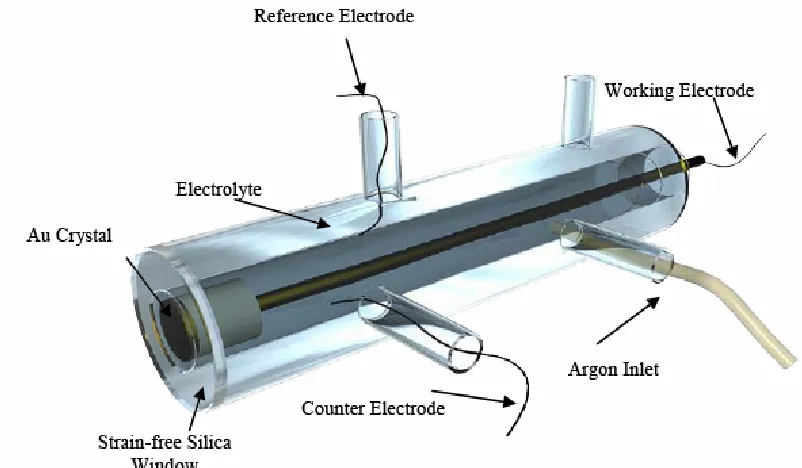
2.3.2: The Electrochemical Cell
Figure 2.11: Schematic of the electrochemical cell used in all potential controlled experiments.
Reproduced with permission from N. Almond [21].
2.3.3: Cyclic Voltammetry
2.4: X-ray Photoelectron Spectroscopy
XPS is employed in this thesis as a sensitive diagnostic tool for the elemental and chemical analysis of adlayers on both Au(110) and CVD grown diamond surfaces. This technique harnesses the phenomena known as the photoelectric effect first detected by Heinrich Hertz in the latter part of the nineteenth century [22] which the eminent physicist James Clerk Maxwell had theorised some fifteen years previously. Einstein, through his famous Nobel prize winning paper of 1905 [23], placed the photoelectric effect in the common conscience by utilising Planck’s quantum theory of black body radiation to propose that if and only if the frequency (ν) of the incident electromagnetic radiation had reached a specific threshold, could an electron spontaneously absorb a quantum of energy and hence be emitted from the material with a measurable kinetic energy (EK). The technique is used extensively as it produces high quality re-producible results which can be interpreted in terms of the elemental composition and electronic structure of the subject sample.
Measurement of EK together with knowing the work function φ of the analyser specific to each XPS instrument enables one to determine the binding energy (EB) of the emitted electrons according to the photoelectric equation:
EK = hν - φ- EB (2.35)
thereby allowing identification of the characteristic energy levels of individual elements to be established.
The binding energy of an electron in a quantised atomic energy level is defined as the amount of energy required for that electron to escape the attractive electrostatic force provided by the atom’s positive nucleus. The work function is defined as the difference in potential energy of an electron between two energy levels described as the Fermi level (EF) and vacuum level (Evac) as shown in Figure 2.12.
number, l is the orbital angular momentum quantum number and j is the total angular
momentum quantum number, j = (l + s) where s is the spin angular momentum
quantum number (± ½). Hence s levels (l = 0) are singlets but all other levels (l > 0)
give rise to doublets.
In a recorded kinetic energy spectrum, the signals from core levels which one expects to be very sharp are broadened into peaks. There are two contributory factors which cause this broadening: (a) the lifetime of the core hole itself as it is governed by the processes that follow photoemission by which the excess energy of the ion state decays [24] (explained below) and takes the form of a Lorentzian contribution while more importantly (b) the instrumental Gaussian resolution function (ΓI) whose origin arises from a combination of broadening effects from both the analyser (ΓA) and monochromator (ΓM) during measurement. The analyser resolution can be calculated from a well characterised feature such as the Fermi edge of Ag whilst the monochromator resolution is dependent upon how well the impingent radiation is focused. The relationship between these contributions is succinctly captured in Equation (2.36):
2 2 2
M A I =Γ +Γ
Γ (2.36)
K. Williams [25] has recently conducted calibration studies on the equipment used in the current work. A reproduction of the tabulated instrumental Gaussian resolution as a function of entrance slit width and pass energy is shown in Table 2.1.
Table 2.1: Gaussian resolution as a function of entrance slit width and pass energy.
6mm slit 4mm slit 2mm slit 1mm circular
aperture 5mm circular aperture Analyser standard
deviation Resolution at a pass energy of
10 eV
0.200 0.133 0.067 0.033 0.167
Analyser standard deviation Resolution
at a pass energy of 20 eV
0.400 0.267 0.133 0.037 0.333
Analyser standard deviation Resolution
at a pass energy of 50 eV
0.884 0.589 0.295 0.147 0.737
Analyser standard deviation Resolution
at a pass energy of 100 eV
2.000 1.333 0.667 0.333 1.667
an electron from a less strongly bound energy level which liberates its excess energy in the form of the kinetic energy of a further (Auger) electron which is excited out of the atom. This process is explained schematically in Figure 2.12 for the case where an L-shell electron minimises the energy of the atom by dropping to the K-shell to fill the core hole. The energy released through this action, EB(K) – EB(L), causes the electron remaining in the L-shell to be emitted and for the purposes of this specific case can be described in X-ray notation as a KLL Auger electron. The kinetic energy of the KLL Auger electron is:
EK = EB(K) – EB(LL)
Figure 2.12: Schematic depiction of different core-hole relaxation processes after initial
excitation with a photoelectron (left), including Auger electron emission (centre) and X-ray fluorescence (right).
As a direct result of excitations in the surface layers by X-rays, photoelectrons are generated from a depth of 10 nm. The excited electrons move through the solid undergoing both inelastic and elastic scattering in which some will escape into the vacuum to be detected by the spectrometer. Only those photoelectrons that have been subject to either elastic or conversely no scattering whatsoever result in the discrete peaks on a spectrum whose energies reflect the quantised shell structure of the sample under investigation. Consequently electrons more loosely bound to the atom in higher shell configurations which escape from the solid without energy loss appear at a very high kinetic energy (or low binding energy) in XPS spectra. This is often labelled the no-loss or primary spectrum. In addition, there will also be intrinsic excitations occurring at the same time as the transfer of energy to the core level electron that appear as characteristic losses. Hence the primary spectrum consists of a peak or peaks together with a tail to higher binding energies that may or may not have significant structure [27]. Moreover, there are electrons that have lost energy through extrinsic inelastic processes as they traverse the solid and these appear as a background which extends from the peak energy to zero kinetic energy. This is called the inelastically-scattered background. A further, secondary, electron cascade background from electron collisions within the material which can result in secondary electron emission from atomic neighbours extends throughout the spectral range but is most intense at kinetic energies < 250 eV. This cascade effect is modest however and since few photoelectric peaks exist at such low kinetic energies it is generally ignored in XPS.
2.4.1: The VSW ESCA Instrument
Figure 2.14: Schematic of the VSW ESCA Spectrometer taken from [27].
Both the preparation and main chambers of the apparatus are each pumped by a turbo pump backed by an alcatel pump which encompasses a molecular drag pump backed by a diaphragm pump. A pneumatic valve on the preparation chamber offers protection against vacuum accidents such as unexpected venting. Additional pumping to reach and sustain the required UHV level is provided by titanium sublimation pumps in each chamber.
2.4.2: Monochromated X-ray Source
source of the Henke design [29]. Thermionic electrons from a tungsten filament are accelerated onto an Aluminium anode held at a high potential of approximately 12.5 kV. The anode is cooled by a water pump of minimum flow rate 5 l/m and also pumped by an ion pump. Both anode and filament shape are carefully designed to produce a sharp focus of e- onto a small spot on the anode thereby generating a sharply focused spot ~ 2 x 3 mm2 in size. Core-level electrons are removed from the K-shell of atoms in the anode when electrons from the tungsten filament impact upon it. Core-hole states created through this process decay through characteristic emission of K-shell X-rays of 1486.6 eV.
A crystal monochromator is housed in a UHV maintained vessel terminating in a 1500 mm flange. An X-ray transparent Mylar window isolates the monochromator vacuum from the main experimental chamber. This window also protects samples from the relatively high pressure in the monochromator chamber caused by outgassing of the X-ray gun while preventing contamination of monochromator crystals through desorption of the specimen surfaces.
Monochromation of the X-rays is suitably attained by first order diffraction of the Al Kα radiation. The diffractor is a 200 mm2 surface consisting of 35 quartz crystals
cut parallel to the (1010) plane while the source, sample and monochromator lie on a 686 mm Rowland circle. The Bragg angle is set to 78.5˚ to satisfy the Bragg condition for first order diffraction of the subject radiation. The crystals themselves are mounted in accordance with Johann geometry providing a radiation spot size in relation to the size of the X-ray source. Mechanical adjustment of the orientation and position of the crystals relative to source and sample is made possible through three precision micrometers on the vacuum housing.
2.4.3: Analysis of Photoelectron Energies
150 mm hemispherical analyser be employed. A six element electrostatic lens which retards photoelectrons helps to focus them onto then entrance slits of the analyser. These electrons are then fed into channel plates to provide a platform for 16 channel detection. As is shown in Table 2.1, there are five choices for entrance slit width: 5 and 1 mm diameter holes and 2 X, 4 X and 6 X 12 mm slits. These can be changed externally along with 4 different pass energies enabling the user to balance resolution with count rate. The analyser has an acceptance angle (α) of 4˚ and the energy resolution is calculated from Equation (2.37):
) 4 2
(
2
0 0
α
+ =
∆
R d E
E (2.37)
where E0 is the energy being analysed (pass energy), d is the chosen slit width and R0 is the mean radius of the hemisphere (150 mm).
The energy scale of the spectrometer can be accurately calibrated enabling detailed binding and Auger energies to be determined. The analyser power supplies are driven by a 0 – 10 V output from a computer controlled DAC. R. Unwin from Scientific Instruments Consultants in 2003 (Version 8.5-D-A) has written software to control analyser voltages and calibration.
Photoelectrons dispersed in energy across the exit focal plane emerge from the analyser and enter microchannel plates. Two channel plates are situated directly beneath the analyser exit slit. Whilst a scan is engaged the channel plates are run sequentially through each energy point on the spectrum meaning that each channel contributes equally to each data point. The effect of this multi-detector array is to greatly improve sensitivity and in conjunction with the monochromated Al Kα source
![Figure 2.1: Comparison of electron escape depth vs light penetration depth in solids [3].](https://thumb-us.123doks.com/thumbv2/123dok_us/8065671.226659/21.612.172.484.471.679/figure-comparison-electron-escape-depth-light-penetration-solids.webp)
![Figure 3.2: Au(110) in UHV displaying the RA profile of the (1x2) reconstruction from [19]](https://thumb-us.123doks.com/thumbv2/123dok_us/8065671.226659/64.612.191.454.401.661/figure-au-uhv-displaying-ra-profile-x-reconstruction.webp)