This is a repository copy of
Influence of doping density on electron dynamics in
GaAs/AlGaAs quantum cascade lasers
.
White Rose Research Online URL for this paper:
http://eprints.whiterose.ac.uk/1695/
Article:
Jovanovic, V.D., Hofling, S., Indjin, D. et al. (5 more authors) (2006) Influence of doping
density on electron dynamics in GaAs/AlGaAs quantum cascade lasers. Journal of Applied
Physics, 99 (10). 103106-(9 pages). ISSN 1089-7550
https://doi.org/10.1063/1.2194312
[email protected] https://eprints.whiterose.ac.uk/ Reuse
See Attached
Takedown
If you consider content in White Rose Research Online to be in breach of UK law, please notify us by
Influence of doping density on electron dynamics in GaAs/ AlGaAs
quantum cascade lasers
V. D. Jovanovića兲
School of Electronic and Electrical Engineering, University of Leeds, Leeds LS2 9JT, United Kingdom
S. Höfling
Technische Physik, Universität Würzburg, Würzburg, Am Hubland D-97080, Germany
D. Indjin, N. Vukmirović, Z. Ikonić, and P. Harrison
School of Electronic and Electrical Engineering, University of Leeds, Leeds LS2 9JT, United Kingdom
J. P. Reithmaierb兲and A. Forchel
Technische Physik, Universität Würzburg, Würzburg, Am Hubland D-97080, Germany
共Received 23 October 2005; accepted 23 February 2006; published online 31 May 2006兲
A detailed theoretical and experimental study of the influence of injector doping on the output characteristics and electron heating in midinfrared GaAs/ AlGaAs quantum cascade lasers is presented. The employed theoretical model of electron transport was based on a fully nonequilibrium self-consistent Schrödinger-Poisson analysis of the scattering rate and energy balance equations. Three different devices with injector sheet doping densities in the range of
共4 – 6.5兲⫻1011cm–2have been grown and experimentally characterized. Optimized arsenic fluxes were used for the growth, resulting in high-quality layers with smooth surfaces and low defect densities. A quasilinear increase of the threshold current with sheet injector doping has been observed both theoretically and experimentally. The experimental and calculated current-voltage characteristics are in a very good agreement. A decrease of the calculated coupling constant of
average electron temperature versus the pumping current with doping level was found. © 2006
American Institute of Physics.关DOI:10.1063/1.2194312兴
I. INTRODUCTION
The idea of electrically pumped intersubband lasers or
quantum cascade lasers 共QCLs兲 as unipolar semiconductor
devices utilizing intersubband transitions in a repetition of identical coupled multi-quantum-well structures was
pio-neered by Kazarinov and Suris.1 However, more than
20 years passed until the experimental realization was
dem-onstrated by Faist et al. at Bell Laboratories on an InP
substrate.2Since then tremendous progress in QCL research
has resulted in bidirectional,3multiwavelength,3,4 ultrabroad-band,5above room temperature continuous-wave共cw兲
opera-tion,6–8 sum-frequency and higher order harmonic
genera-tion,9–11 and fully integrated electrically pumped Raman
lasers.12 Moreover, laser operation has been reported on
other material systems, i.e., AlGaAs on a GaAs substrate13
and Al共Ga兲Sb on InAs.14Devices with Sb-containing barriers on both InAs substrate14–16 as well as on InP substrate17–19 are promising for either increasing the electron confinement or reducing the emission wavelength, and above room tem-perature pulsed operation on both substrates was recently reported.16,18
Since the realization13 of the GaAs-based quantum cas-cade laser, an impressive extension of the attainable infrared
frequency range has been achieved and can be operated at
wavelengths as long as 160m.20The design of QCLs based
on GaAs/ AlGaAs can be made very flexible by varying the Al content due to naturally occurring near lattice matched material system across the full range of Al contents. Hence,
following the first terahertz QCL,21 several laser designs
based on 15% Al content in the barriers were presented, ap-proaching high temperature pulsed operation22 共137 K兲 and above23 or close to24 liquid nitrogen temperature cw opera-tion.
GaAs-based QCLs emitting in the midinfrared spectral region have so far used Al contents of 33%,13,25 45%,26–28 and 100%,29–31respectively. Pulsed room temperature opera-tion has been reported only for designs with 45% Al
content26–28 except for one design employing AlAs barriers
and monolayers of InAs deposited at the antinode of the electron wave functions in order to improve the electron
confinement.30Achieving cw operation in midinfrared
GaAs-based QCLs is a very challenging task due to the relatively high threshold current densities. Nevertheless, cw operation has been reported29,32,33 with operating temperatures up to 150 K.33
However, the output characteristics of midinfrared GaAs-based devices are still rather poor in comparison to InP-based midinfrared QCLs, which can lase in cw regime at
room temperature.6 For further improvements, a detailed
knowledge of crucial design parameters as well as an under-standing of relevant physical limitations of particular designs and further investigation of the influences of relevant physi-a兲Present address: Lehman Brothers, 25 Bank Street, London E14 5LE,
United Kingdom; electronic mail: [email protected]
b兲Present address: Technische Physik, Insititute for Nanostructure Technolo-gies and Analytics, University of Kassel, Heinrich-Plett-Strasse 40, D-34132 Kassel, Germany.
cal and technological parameters are highly desirable. To-gether with experimental investigations, a systematic and compact theoretical modeling is a necessary step towards improvements of the existing structures and the understand-ing of physical processes within. These include Monte Carlo
simulation,34–37 nonequilibrium Green’s function
forma-lism,38,39as well as self-consistent rate equations model.40,41 The doping level in the active region is an important parameter with particular influence on the dynamic working range of QCLs. Until now, very few experimental investiga-tions have been presented including the influence of the
in-jector doping on InP-based42–44 and GaAs-based45–48 QCL
threshold currents.
Due to the superior device performance of midinfrared devices with 45% Al content there is a demand for a com-prehensive experimental and theoretical analysis of these de-signs. In this work, we report such an investigation of three-quantum-well design26in which the influence of the injector doping density on the carrier dynamics is analyzed.
II. THE QCL MODEL
Electron transport in QCLs was simulated within the framework of a fully self-consistent scattering theory
approach.40,41 For that purpose, the QCL was assumed to
consist of a large number of periods forming a perfectly pe-riodic cascade withNbound or quasibound states assigned to each period. The latter is justified by excellent localization properties of the confining potential in QCLs. Hence, the space and energy shift invariance of the potential enforce the same type of translation symmetry on the solutions of the Schrödinger equation, i.e., if the⌿共z,E兲is a solution of the
eigenvalue problem then ⌿共z+L,E+⌬V兲, where L is the
length of the period, and⌬Vis the potential drop across the period, will also be a solution as well. Furthermore, the scat-tering processes follow the same trend, i.e., the intraperiod scattering rate between equivalent states in any two periods is equal共Wi,j=Wi+kN,j+kNk= 1 , 2 , . . ..兲. Also, the shift
invari-ance of the inter-period scattering between different periods requires that Wi−kN,j=Wi,j+kN k= 1 , 2 , . . . . In order to reduce
the computational cost of calculating a large number of scat-tering rates, the model was embedded into a “tight-binding”-like picture, assuming that each period interacts with only a few of its nearest neighbors. Based on the symmetry rules in a cascade, a limited number of scattering rates between the states of a single period and its following P nearest neigh-bors needs to be calculated. Therefore, the total number of scattering rates is dependent on the number of chosen neigh-bors and bound states within the period state set and is equal toN2共2P+ 1兲−N. With the scattering rates known, a
steady-state nonequilibrium electron distribution over quasidiscrete states of the injector/collector miniband and over states of the active region can be calculated by solving a system of rate equations given as
dni
dt =j=1,
兺
j⫽iN
njWj,i−ni
兺
j=1,j⫽i N
Wi,j
+
兺
k=1
P
兺
j=1,j⫽i N
兵nj关Wj,i+kN+Wj+kN,i兴
−ni关Wi+kN,j+Wi,j+kN兴其. 共1兲
Owing to the ultrafast nature of intersubband relaxation processes the system can be solved in the steady-state regime
assuming d/dt= 0. The system comprises of N− 1 linearly
independent equations completed with the particle conserva-tion law, i.e., 兺ini=Ns, where Ns is the total sheet electron
density in each period. As the scattering rates are electron
density dependent 共i.e., usually averaged assuming
Fermi-Dirac distributions over subbands兲, the solution of the system has to be found in the self-consistent manner, until the carrier
distribution converges.40,41 The physical meaning of the i
⫽j requirement in Eq. 共1兲 is that intrasubband scattering processes are not influencing the electron population over states. However, such processes will later become relevant in the discussion of the electron heating in QCLs.
In order to simulate the influence of the injector doping density on the output characteristics of QCLs, the model was extended to include the effects of the dopant position and electron distribution on the electronic structure and dynam-ics. Commonly, the effective band profile including the elec-trostatic potential is calculated by iteratively solving the Schrödinger and the Poisson equations until the electronic structure converges. However, in the case of a highly non-equilibrium system such as a QCL共i.e., working in the high current injection regime兲, an electron distribution is not pre-defined, and in each step of the iterative procedure it has to be separately estimated. Hence, the electrostatic potential is dependent on the transport properties of the structure and both the Schrödinger and Poisson equations as well as the system of scattering rate equations关Eq. 共1兲兴are intrinsically coupled. As a consequence, the convergence of both pro-cesses 共self-self-consistency兲is required for the accurate so-lution of the electron distribution over subbands. In the low bias regime applied across the QCL periods, i.e., in the lasing subthreshold, the carrier distribution over subbands becomes close to equilibrium and a common Fermi level across the structure can be assumed. In such a case, the electronic trans-port does not influence the electrostatic potential, and the
scattering rate equations are decoupled from the
Schrödinger-Poisson solver. Hence, the calculation becomes much simpler and is usually employed in the literature. How-ever, the subthreshold regime does not reflect the real nature of the electronic transport in QCLs and cannot deliver the necessary insight into the lasing capabilities in case of a high doping level. In order to explore the influence of doping density on the above threshold QCL regime, the calculation in a fully self-self-consistent manner, described above, is re-quired.
One should note that the electrostatic potential given as a solution of the Poisson equation is due to the quasiperiodic
nature of the electron and donor distribution also periodic and needs to be found only for a single period and space shifted to map the whole structure.
A. Electron temperature
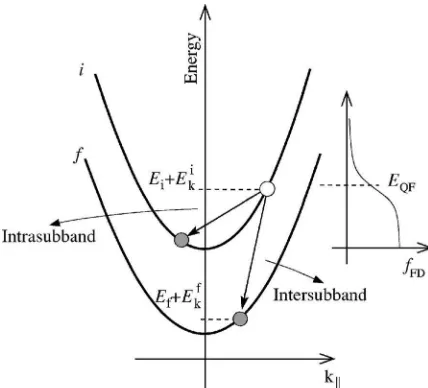
Owing to the various elastic or inelastic scattering inter-actions, electrons transfer their kinetic energy between sub-bands. A gain or loss of the total energy of the subband can be modeled in terms of the subband electron temperature, as previously done in the literature.49,50This assumes that the electron distribution in a subband is thermalized and thus, the extra kinetic energy of the electrons is quickly redistrib-uted, and the distribution is rethermalized. The rate at which the kinetic energy is transferred between the subbands can be modeled in the rate equation framework, in a fairly similar manner as the electron densities over subbands. Hence, the electron in theith state scattering into thefth state will result in a loss of energy in theith state equal to its kinetic energy Eki. An increase of energy in thefth state based on the energy conservation law then reads
Ekf=Ei−Ef+␦E+Ek i
, 共2兲
where ␦E is the energy of the scatterer, and Ei−Ef is the
“nonkinetic” energy gain/loss owing to the different energies of the subbands 共Fig. 1兲. For elastic 共electron-electron, im-purity, etc.兲 and inelastic 共electron-phonon兲scattering inter-actions relevant in most QCLs, the energy of the scatterer can be written as
␦E=
冦
ELO for phonon absorption process
−ELO for phonon emission processes
0 for elastic scattering processes,
冧
共3兲
where ELO is the LO-phonon energy. Two different energy
rates corresponding to thei→f transition can be defined as wi+,f, representing the rate at which the energy of thefth state increases, andwi−,f, representing the rate at which the energy of the ith state decreases. Therefore, the equation defining the total energy rate of the subband reads
dEf
dt =
兺
iniwi,f
+
−nf
兺
iwf−,i. 共4兲
The rate at which the energy of the final state increases共wi+,f兲 is equal to the product of the “incoming” kinetic energy关Eq.
共2兲兴and the scattering rate corresponding to that energy state
共i.e., in-plane wave vector兲 Wi,f共Ek i兲
. The total rate can be found by averaging the product 具EkiWi,f共Ek
i兲典
over Fermi-Dirac distribution with respect to the subband temperatureTi
and taking into account the Pauli exclusion principle as
wi+,f=兰0
⬁E
k fW
i,f共Ek i
,Ti兲fFD共EQF
i
,Ti兲关1 −fFD共EQF
f
,Tf兲兴dEk i
兰0
⬁f
FD共EQF
i
,Ti兲dEk
i , 共5兲
whereEQFi is the quasi-Fermi levels of the electron distribu-tion on theith state. By substituting the expression forEki the latter reads
wi,f
+
=共Ei−Ef+␦E兲Wi,f
+兰0
⬁E
k i
Wi,f共Ek i
,Ti兲fFD共EQF
i
,Ti兲关1 −fFD共EQF
f
,Tf兲兴dEk i
兰0
⬁f
FD共EQF
i
,Ti兲dEk
i ,
共6兲
whereWi,fis the average scattering rate. Similarly, the rate at which the energy of theith state decreases共wi−,f兲follows
wi−,f=兰0
⬁E
k i
Wi,f共Ek i
,Ti兲fFD共EQF
i
,Ti兲关1 −fFD共EQF
f
,Tf兲兴dEk i
兰0⬁fFD共EQF
i
,Ti兲dEk
i , 共7兲
Hence, thewi+,f andwi−,f are related as
wi+,f=共Ei−Ef+␦E兲Wi,f+wi,f
−
. 共8兲
Although, not explicitly present in the particle rate equa-tion, the intrasubband scattering 共wi+,i=wi−,i兲 has to be ac-counted for in the energy balance equation as the energy of an electron in the subband can change due to interaction with the lattice or due toi,j→i,j-type electron-electron interac-tion, and thus the intrasubband scattering can be a mecha-nism of electron cooling or heating.
Hereafter, the balance equation is derived for the cascade in the tight-binding approximation. If the energy gain/loss rate is balanced, the total energy does not change in time,
i.e., d/dt= 0, and thermalization of each subband can be
characterized via a unique electron temperature共Ti兲. Hence,
assumingPnearest neighbors, the Eq.共4兲can be rewritten as
dEf
dt = 0 =
兺
i=1N
niwi,f
+
−nf
兺
i=1N
w−f,i+
兺
k=1
P
兺
i=1
N
关ni共wi,f+kN
+
+wi++kN,f兲
−nf共w−f+kN,i+w−f,i+kN兲兴, 共9兲
wherewi+,f andw−i,f are given by Eqs.共8兲 and共7兲. Equations
共9兲and共1兲form a system of 2Nnonlinear equations yielding
N subband concentrations and N electron temperatures.
However, recent experimental51 and theoretical work50 justi-fied the use of a single共average兲electron temperature共Te兲in
[image:4.612.64.278.48.242.2]the midinfrared QCLs. Furthermore, this considerably re-duces the computational cost of solving of a nonlinear prob-lem. Hence, the summing of the particular balance equations for each subband reads
共10兲
where the physical meaning of the terms in the equation equal to zero, can be understood as the balance between the kinetic energy loss of theith and the energy gain of thefth state owing to thei→f scattering. Hence, Eq.共10兲does not comprise the integral terms. As the energy separation be-tween the states of the different periods can be written in terms of the single period energies and the potential drop across the period共⌬V兲, i.e.,Ei+kN=Ei+k⌬V, the final form of
the single temperature balance equation reads
兺
f=1
N
兺
i=1
N
ni共Ei−Ef+␦E兲Wi,f+
兺
f=1N
兺
k=1
P
兺
i=1
N
ni关共Ei−Ef−k⌬V
+␦E兲Wi,f+kN+共Ei−Ef+k⌬V+␦E兲Wi+kN,f兴= 0.
共11兲
The equation is coupled with the scattering rate equation
关Eq. 共1兲兴, and as such, needs to be incorporated into the self-consistent procedure and evaluated in each iteration. That also adds on the complexity of the problem as the con-vergence of the electron temperature becomes a necessary requirement as well.
B. Output parameters
Having the electron distribution and temperature over subbands, physical observables such as current density, frac-tional injection, gain, and threshold current can be estimated. The current density in the QCL cascade is defined as49
J=
兺
k=1
P
兺
i=1
N
兺
j=1
N
kni共Wi,j+kN−Wi+kN,j兲, 共12兲
where the first term presents forward scattering into the states of the neighboring periods and the second term pre-sents backscattering. The definition of the current density can also be used for estimating fractional injection as a ratio of the current injected into the upper laser level and the total current through the QCL.
In the two level approximation, the modal gain can be expressed as
G共兲= e
2
cn0⑀0L
兺
i=1N
兺
f=1
N
ni兩zi,f兩2sgn共Ei−Ef兲L共,兩Ei−Ef兩兲
+
兺
k=1
P
兺
i=1
N
兺
f=1
N
ni兵兩zi,f+kN兩2sgn共Ei−Ef−k⌬V兲
⫻L共,兩Ei−Ef−k⌬V兩兲
+兩zi+kN,f兩2sgn共Ei−Ef+k⌬V兲L共,兩Ei−Ef+k⌬V兩兲其,
共13兲
wheren0is the refractive index,Lis the length of a period,
L共·兲 is the Lorentzian assumed to describe well gain broad-ening, and “sgn” denotes the sign function of the argument. The modal gain is then equal toGM=g⌫.
Having the current dependence of the modal gain, the threshold current can be evaluated based on a well-known formula: GM共Jth兲=␣W+␣M, where the ␣M and ␣W are the
mirror and waveguide losses, respectively.
C. Electronic structure and scattering calculation
The subband energies and wave functions were calcu-lated by solving the envelope function Schrödinger equation in an effective mass approximation with conduction band dispersion nonparabolicity taken into account via Kane’s two-band model of the energy-dependent effective mass. The Schrödinger equation was solved for three full QCL periods. Clearly, the states confined mostly in the central period are calculated with better accuracy than states in other periods, owing to distant boundary conditions, and therefore these states have been taken to form a period state set. Based on the space and energy shift invariance, they were afterwards used to create the states of all other periods. The relevant scattering mechanisms that have been taken into account are based on phonon, electron, and electron-impurity interactions. The latter of which can be important at high doping levels. The scattering rates were calculated us-ing Fermi’s golden rule and averaged over the in-plane wave vector assuming Fermi-Dirac distributions over subbands. For calculating the electron-LO-phonon scattering, bulk pho-non modes were assumed, which is widely used in the litera-ture owing to a good agreement with the experiment for
QCL structures.34,38,40,47 Single subband screening of the
electron-electron scattering was accounted for in the
frame-work of the random phase approximation.52 Based on a
sample calculation, the acoustic phonon scattering was found to be a few orders of magnitude smaller than the LO-phonon scattering due to a large subband energy separation and a relatively high operating temperature and as such, assumed to be negligible.
III. DEVICE FABRICATION AND CHARACTERIZATION
For the experimental investigations, three wafers based on a three-quantum-well design26 with doping levels of 4.1,
5.2, and 6.5⫻1011 cm−2 were grown in series with a solid
source molecular beam epitaxy共MBE兲system. The group III
elements aluminium and gallium as well as then-type dopant
silicon were provided by conventional effusion cells共a dual filament cell was used for Ga兲. For arsenic a valved cracker
cell was used in As4 growth mode. The MBE system
cali-bration and the layer quality confirmation were performed with high resolution x-ray diffraction and scanning electron microscopy. The layer structures were grown at a pyrometer
temperature of 590 ° C on the 共001兲 plane of highly doped
GaAs:Si substrates with a GaAs growth rate of 0.75m / h
for the entire structure. The active regions comprise 48 cas-caded stages embedded in a symmetrically grown plasmon
enhanced waveguide53,54 with 3.8m thick low doped 共4
⫻1016cm−3兲 and 1.2m highly doped 共4⫻1018cm−3兲
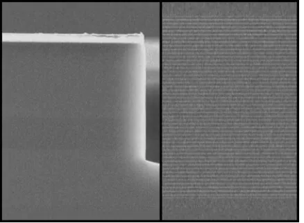
GaAs layers. On the left of Fig. 2, a scanning electron
mi-croscopy 共SEM兲 image of the laser facet is depicted. The
slightly darker section at the bottom of the ridge can be iden-tified as the active region, which is shown in a magnified SEM image on the right of Fig. 2.
Optimized arsenic fluxes were used for the growth of the active region layers and the waveguide layers.45 The fluxes
used for the waveguide 关V/III beam equivalent pressure
共BEP兲ratio of 35兴 and the active region layers 共V/III BEP ratio of 50 for GaAs layers, correspondingly less for AlGaAs layers兲result in high-quality layers with smooth surfaces and low defect densities. Layer structures grown under these
con-ditions exhibit threshold current densities of 2.9 kA/ cm2
共8.0 kA/ cm2兲at 80 K共240 K兲and maximum operation
tem-peratures of around room temperature. In contrast, when the growth was performed with a constant III/V BEP ratio of 65 for both the waveguide and active region GaAs layers, we have observed increased threshold current densities of 5.1 kA/ cm2 共19 kA/ cm2兲 at 80 K 共240 K兲 and the maxi-mum operation temperature decreased to about 255 K.
In order to avoid current spreading and to achieve good
lateral optical confinement, 18 to 34m wide ridge
wave-guide lasers were manufactured from the wafers by etching through the active region. For this purpose, the thinned wa-fers were processed by standard optical lithography and elec-tron cycloelec-tron resonance reactive ion etching in an Ar/ C12
plasma. The bottom contacts 共Au/ Ge/ Ni/ Au兲 were
depos-ited and alloyed, while the top contact共Cr/ Pt/ Au兲 was not alloyed and evaporated together with a thick Ni layer which served as the etch mask. Devices with 1 mm long cavities and uncoated facets were mounted episide up on copper heat sinks and wire bonded. For characterization, the QCLs were installed in a continuous flow helium cryostat and operated under pulsed conditions. All electro-optical measurements were made with 100 ns long pulses and repetition rates of about 500 Hz. The light output characteristics were
deter-mined with a fast mercury cadmium telluride共MCT兲
detec-tor. Spectral characteristics were measured with a slow MCT detector in a Fourier transform infrared spectrometer setup in rapid scan mode.
IV. RESULTS AND DISCUSSION
The electronic and optical characteristics of the 45%
Al⬃9m QCL design26 have been investigated for the
se-ries of injector doping densities 4.1⫻1011, 5.2⫻1011, and
6.5⫻1011 cm−2. Fully self-consistent calculations were
per-formed for lattice temperatures of 80 and 240 K. The calcu-lated band profile and wave functions squared for
conven-tional doping of 4.1⫻1011cm−2 at T= 80 K are shown in
Fig. 3. For the moderate doping conditions, the self-consistent band bending due to the specific electron distribu-FIG. 2. SEM pictures of a cleaved facet of a processed ridge waveguide
[image:6.612.326.545.46.209.2]structure共left兲and of the corresponding active region with 48 stages共right兲. The slightly darker region at the bottom of the ridge structure can be iden-tified as the active region.
[image:6.612.65.284.50.211.2]tion is not very prominent, however, when higher doping is used, the band profile changes. That is especially important in the working regime around the resonant alignment be-tween ground injector and upper laser levels.
As an example, the typical light output characteristics of
a 1.5 mm long device with 4.1⫻1011cm−2 injector doping
level at several heat sink temperatures are shown in Fig. 4. As discussed in detail below, devices with an injector doping of 4.1⫻1011cm−2 exhibit consistently lower threshold cur-rent densities compared to devices with higher doping con-centrations.
The measured temperature dependence of the threshold current density of a corresponding 1 mm long device is given in Fig. 5. It is interesting to note that at 80 K, the threshold current density amounts to 2.9 kA/ cm2, which is a factor of 2 lower than that measured in devices with a sheet carrier concentration of 6.5⫻1011cm−2. The inset of Fig. 5
[image:7.612.325.544.47.424.2]displays the typical Fabry-Perot emission spectrum of a de-vice just above threshold taken at 80 K.
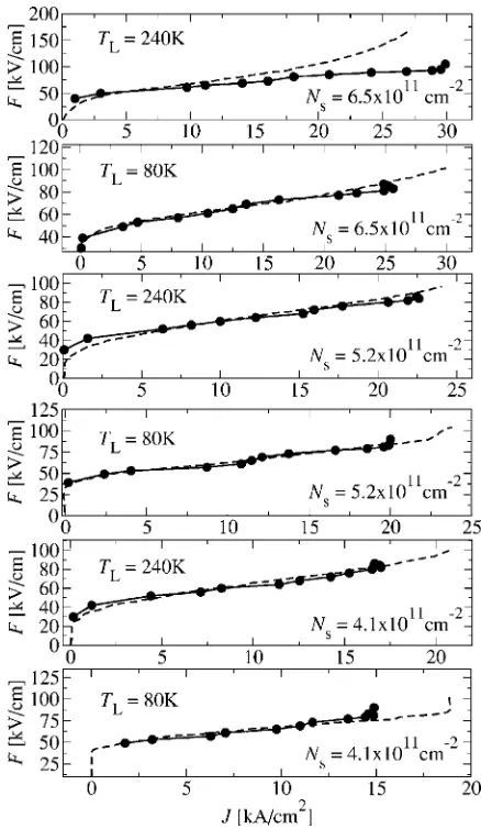
Figure 6 shows the theoretical共normal line and circles兲 and experimental 共dashed line兲 field-current density charac-teristics for the analyzed injector doping densities at the lat-tice temperatures of 80 and 240 K. The calculatedI-Vcurves have been shifted by a voltage drop across the waveguide and contacts, by fitting to experimental data found to be 2 V
at 80 K and 2.6 V at 240 K. An excellent agreement, both quantitatively and qualitatively, between the simulation and the experimental measurements was found. There is an espe-cially good agreement in the slope of theI-Vcurves, giving a good match for the structure’s differential resistivity.
However, the theoretical maximal current density 共just before the current saturation兲 is generally lower than mea-sured. For example, in the case of the “4.1” device at 80 K it
is around 14 kA/ cm2, which is somewhat lower than the
measured value of 19 kA/ cm2. That could be explained with
leakage mechanisms existing in the real QCL devices and not accounted for in the calculations. Furthermore, a certain dis-crepancy was observed between the calculated and measured
I-V curves at higher fields for the injector doping of 6.5
⫻1011cm−2at 240 K. In that particular case, the
experimen-tal measurement is showing a larger differential resistivity than expected, probably owing to imperfect contacts.
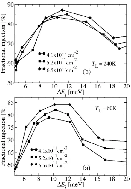
The fractional injection is calculated as a function of the energy spacing between the upper laser level and the lowest injector state共⌬El兲 and presented in Fig. 7 for different
[image:7.612.64.287.47.205.2]in-jector doping densities at 80 and 240 K. The bell-like shape of the fractional injection is observed for both temperatures, FIG. 4. Typical light output characteristics up to 280 K for a 1.5 mm long
device with 4.1⫻1011cm−2injector sheet doping level.
FIG. 6. Simulated current density-field characteristics for the three doping densities共4.1⫻1011, 5.2⫻1011, and 6.5⫻1011cm−2兲at the lattice tempera-tures of 80 and 240 K共normal line and circles兲. The voltage drop across the waveguide and contacts of around⬃2V was assumed. The measured current density-field characteristics are presented with dashed lines.
FIG. 5. Dependence of the threshold current density on temperature mea-sured for the 1 mm long device. The inset shows a typical emission spec-trum just above threshold taken at 80 K.
[image:7.612.65.283.568.721.2]showing a maximum in the range of ⌬El between 10 and
12 meV. In the range below 10 meV the fractional injection drops rapidly, due to an enhanced backfilling from the upper laser level into the lowest injector state in the conditions close to resonance. Moreover, as this occurs at higher electric fields, the parasitic current channels via higher injector states and a quasicontinuum exist, decreasing a fraction of the total current going through the upper laser level. An increase of the fractional injection with doping density was observed at
80 K, ranging from ⬃75% at 4.1⫻1011 cm−2 to ⬃85% at
6.5⫻1011cm−2. This is a consequence of enhanced injection from the lowest injector state into the upper laser level via electron-electron scattering in the higher doping regime. However, at 240 K the increase of the fractional injection with doping is not pronounced, as the scattering rates be-come less sensitive to the band filling at the higher tempera-tures.
The electron temperature in the single temperature ap-proximation, calculated as a function of current density at 80 and 240 K, for different doping densities is presented in Fig. 8. The dependences are well fitted by a quadratic function
共dashed lines兲. However, for the range of working current densities, the quadratic bowing is rather small, thus a linear
functional form can be adopted50 and characterized by a
electron temperature-current coupling constant. For a fixed value of the current density, a decrease of the electron tem-perature with doping has been calculated. A more
macro-scopic explanation can be presented in terms of an effective decrease of input electrical powerPE, i.e., the same value of
the current density at higher doping corresponds to the lower applied bias than in case of a lower doping共see Fig. 7兲. Also, the power per electron decreases as the number of electrons increases. Hence, for the same current density, the electrons in the QCL, in the higher doping regime, need to heat up less than for lower doping, in order to facilitate a LO-phonon emission and an efficient heat dissipation. This was con-firmed by calculating the ratio between the relative increase in electron temperature and power of each individual elec-tron 共Te−TL兲/共PE/Ns兲 which shows almost constant
behav-ior for all doping levels. Consequently, the coupling constant
drops with increased doping from 10.3 K / kA cm−2 at 4.1
⫻1011cm−2 to 7.1 K / kA cm−2 at 6.5⫻1011cm−2 at 80 K
and from 22.2 K / kA cm−2 at 4.1⫻1011cm−2 to
14.2 K / kA cm−2 at 6.5⫻1011cm−2 at 240 K. The value at
4.1⫻1011 cm−2 at 240 K is in excellent agreement with
re-cently published experimental value of ⬃28 K / kA cm−2
determined from microprobe photoluminescence measure-ments,51but somewhat larger共⬃50%兲than the first
theoret-ical prediction reported earlier,50 due to more scattering
[image:8.612.326.546.45.355.2]mechanisms taken into account in this calculation. The maxi-mal value of the electron temperature, which corresponds to the current density just before saturation, is found to increase linearly with doping. The evaluated increase was around FIG. 7. Fractional injection as a function of the energy difference between
[image:8.612.64.283.46.361.2]the upper laser level and the lowest injector state calculated for the three doping densities of 4.1⫻1011cm−2共circles兲, 5.2⫻1011cm−2共squares兲, and 6.5⫻1011cm−2 共diamonds兲 at the lattice temperatures of 共a兲80 and 共b兲 240 K.
40 K 共i.e. 17%兲at 80 K in comparison with⬃20 K 共6%兲at 240 K. The latter is due to reduced LO-phonon scattering sensitivity to doping density change at high temperatures.
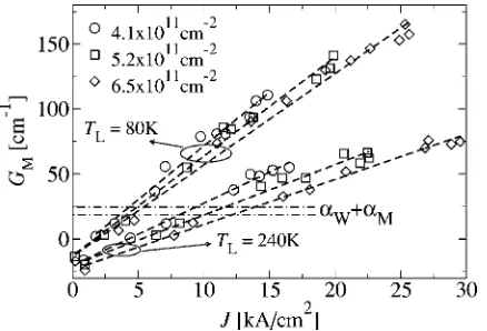
The lasing performance of the QCLs has been theoreti-cally investigated by calculating the modal gain as a function of the current density 共Fig. 9兲. The waveguide parameters
共losses␣Wand confinement factor⌫兲 were calculated using
the transfer matrix approach combined with the Drude model for the material parameters. Due to a greater number of pe-riods in the QCL stack共48兲, the calculated confinement fac-tor is slightly higher than in the original structure by Page et al.,26ranging between 0.37 for 4.1⫻1011cm−2to 0.34 for
6.5⫻1011cm−2. However, the estimated waveguide losses
are quite similar and they are in range between ␣W
=共15– 19兲cm−1, see dot-dashed lines in Fig. 9 where the mirror losses are assumed to be␣M⬇6 cm−1. The full widths
at half maximum 共FWHM兲 of the electroluminescence line
were taken26 to be 12 meV at 80 K and 22 meV at 240 K
and assumed to vary linearly by 1 meV in total in the range of examined doping densities. As expected, the gain exhibits quasilinear behavior and can be fitted by a linear function
共Fig. 9兲up to the current saturation. For both temperatures of 80 and 240 K, the slope of the gain共modal gain coefficient兲 decreases with an increase in doping. That is due to a chang-ing interplay between the decrease in the lower laser level extraction efficiency共e.g., the lifetime at 80 K was reduced by 20%, from 0.34 to 0.28 ps in the examined range of dop-ing兲, decrease of the mode confinement factor, and increase of the FWHM of the luminescence. The latter can especially deteriorate the laser performance at higher temperatures,
where the gain margins are already quite narrow 共see gain
coefficient at 240 K in Fig. 9兲.
Knowing the modal gain dependence on the current den-sity, a threshold current density 共Jth兲 can be estimated. An
excellent agreement with the experimental data was found, with an average discrepancy of around 5%, as shown in Fig. 10. The experimental value of the threshold current at 6.5
⫻1011cm−2 at 240 K was slightly higher than calculated,
which is consistent with the previous discussion on the large differential resistivity exhibited by this particular QCL de-vice. One should note that a simple threshold current esti-mate based on the unity injection approximation in the
simple three-level QCL model, commonly used in
literature,13 does not exhibit a good agreement with the ex-periment. For both temperatures of 80 and 240 K, the thresh-old current density dependence on injector doping level can be characterized by a linear function of the form Jth共Ns兲
⫻共kA/ cm2兲=J
th共4.1兲+␥共Ns− 4.1兲, where Ns is given in
1011cm−2. The calculated slope of the theoretical linear fit
共dashed line on Fig. 10兲 was ␥⬃0.77 kA at 80 K and ␥
⬃2.35 kA at 240 K, which is in a good agreement with the
experimentally obtained ␥⬃0.91 kA at 80 K and ␥
⬃2.91 kA at 240 K. The significantly larger ␥can be
asso-ciated with a considerably smaller gain coefficient at 240 K than at 80 K as well as a further drop due to an increased doping level. Having in mind the increase of the threshold current shown in Fig. 10 but also an increase of the satura-tion current with increased doping, one could consider the optimal value for the doping level for particular application purposes. Recently, it has been argued that in a particular QCL design “optimal” injector doping is suggested to be between 6⫻1011and 8⫻1011cm−2in order to achieve sig-nificant gain and at the same time avoid the considerable increase in the threshold current.55
The theoretical model together with the experimental and numerical analysis presented above clearly show that doping density variations can play an important role in sign and optimization of future high-performance QCL de-vices. This includes reduction of the threshold current and prolonged operation before saturation. Particularly, the lin-earized empirical formula for threshold current dependence
on doping density can help inad hocoptimization of GaAs
devices in the midinfrared. Furthermore, insight into micro-scopic processes governing the electronic transport in QCLs such as electron heating and their connection to density of carriers can lead to increase in the dynamic range of lasing and deliver enhance flexibility in possible applications. Fi-nally, the results presented in this paper can be applied and proved to be of considerable importance in the design and growth of long-wavelength and THz QCLs.
V. CONCLUSIONS
[image:9.612.325.545.45.203.2]We have presented a detailed experimental and theoreti-cal study of the impact of injector doping densities on the FIG. 9. Calculated modal gain for three injector doping densities at 80 and
at 240 K. Dot-dashed lines represent the range of calculated total losses. FIG. 10. Simulated threshold current density 共circles兲and corresponding experimental measurements共squares兲 as functions of the injector doping density at the temperatures of 80 and 240 K. The linear fits of theoretically obtained values are represented by dashed lines.
[image:9.612.66.285.48.197.2]output characteristic and carrier heating in GaAs/ AlGaAs midinfrared QCLs. The employed theoretical model is based on a fully nonequilibrium Schrödinger-Poisson analysis of the coupled scattering rate and kinetic energy balance
equa-tions with all relevant electron-LO-phonon,
electron-electron, and electron-ionized impurity interactions taken into account. Experimental analysis shows substantial reduc-tion of the threshold current, particularly at higher tempera-ture, when optimized arsenic fluxes were used during the growth procedure. The increase of the threshold current with doping level was characterized as quasilinear dependences with a very good agreement between calculations and experi-mental data.
ACKNOWLEDGMENTS
The authors would like to thank R. W. Kelsall, M. Gie-hler, and V. Spagnolo for useful discussions and M. Wagen-brenner and T. Demarczyk for expert technical assistance. Thanks go to J. Seufert of Nanoplus, Nanosystems and Tech-nology GmbH for mounting the devices. The theoretical
work in Leeds is partially supported by EPSRC共UK兲 and
ORS共UK兲. Experimental work at Universität Würzburg was
partially supported by the German Federal Ministry of Edu-cation and Research共project “Quankas”兲.
1
R. Kazarinov and R. Suris, Sov. Phys. Semicond. 5, 707共1971兲.
2
J. Faist, F. Capasso, D. L. Sivco, C. Sirtori, A. L. Hutchinson, and A. Y. Cho, Science 264, 553共1994兲.
3
C. Gmachl, A. Trediccuci, D. L. Sivco, A. L. Hutchinson, F. Capasso, and A. Y. Cho, Science 286, 749共1999兲.
4
C. Gmachl, D. L. Sivco, J. N. Baillargeon, A. L. Hutchinson, F. Capasso, and A. Y. Cho, Appl. Phys. Lett. 79, 572共2001兲.
5
C. Gmachl, D. L. Sivco, R. Colombelli, F. Capasso, and A. Y. Cho, Nature
共London兲 415, 883共2002兲.
6
M. Beck, D. Hofstetter, T. Aellen, J. Faist, U. Oesterle, M. Ilegems, E. Gini, and H. Melchior, Science 295, 301共2001兲.
7
A. Evans, J. S. Yu, J. David, L. Doris, K. Mi, S. Slivken, and M. Razeghi, Appl. Phys. Lett. 84, 314共2004兲.
8
A. Evans, J. S. Yu, S. Slivken, and M. Razeghi, Appl. Phys. Lett.85, 2166
共2004兲. 9
J.-Y. Bengloan, A. De Rossi, V. Ortiz, X. Marcadet, M. Calligaro, I. Mau-rin, and C. Sirtori, Appl. Phys. Lett. 84, 2019共2004兲.
10
C. Gmachl, A. Belyanin, D. L. Sivco, M. L. Peabody, N. Owschimikow, A. M. Sergent, F. Capasso, and A. Y. Cho, IEEE J. Quantum Electron.39,
1345共2003兲. 11
T. S. Mosely, A. Belyanin, C. Gmachl, D. L. Sivco, M. L. Peabody, and A. Y. Cho, Opt. Express 12, 2972共2004兲.
12
M. Troccoli, A. Belyanin, F. Capasso, E. Cubukcu, D. L. Sivco, and A. Cho, Nature共London兲 433, 845共2005兲.
13
C. Sirtori, P. Kruck, S. Barbieri, P. Collot, J. Nagle, M. Beck, J. Faist, and U. Oesterle, Appl. Phys. Lett. 73, 3486共1998兲.
14
K. Ohtani and H. Ohno, Jpn. J. Appl. Phys., Part 2 41, L1279共2002兲.
15
K. Ohtani, K. Fujita, and H. Ohno, Jpn. J. Appl. Phys., Part 2 43, L879
共2004兲. 16
R. Teissieret al., Appl. Phys. Lett. 85, 167共2004兲.
17
Q. Yang, C. Manz, W. Bronner, Ch. Mann, L. Kirste, K. Köhler, and J. Wagner, Appl. Phys. Lett. 86, 131107共2005兲.
18
Q. Yang, C. Manz, W. Bronner, L. Kirste, K. Köhler, and J. Wagner, Appl. Phys. Lett. 86, 131109共2005兲.
19
D. G. Revin, L. R. Wilson, E. A. Zibik, R. P. Green, J. W. Cockburn, M. J. Steer, R. J. Airey, and M. Hopkinson, Appl. Phys. Lett. 85, 3992
共2004兲. 20
D. Scalari, S. Blaser, J. Faist, H. Beere, E. Linfield, D. Ritchie, and G. Davies, Phys. Rev. Lett. 93, 237403共2004兲.
21
R. Köhleret al., Nature共London兲 417, 156共2002兲.
22
B. S. Williams, S. Kumar, H. Callebaut, Q. Hu, and J. L. Reno, Appl. Phys. Lett. 83, 5142共2003兲.
23
S. Kumar, B. S. Williams, S. Kohen, Q. Hu, and J. L. Reno, Appl. Phys. Lett. 84, 2494共2004兲.
24
S. Barbieri, J. Alton, H. E. Beere, E. H. Linfield, and D. A. Ritchie, Appl. Phys. Lett. 85, 1674共2004兲.
25
S. Barbieri, C. Sirtori, H. Page, M. Stellmacher, and J. Nagle, Appl. Phys. Lett. 78, 282共2001兲.
26
H. Page, C. Becker, A. Robertson, G. Glastre, V. Ortiz, and C. Sirtori, Appl. Phys. Lett. 78, 3529共2001兲.
27
S. Anders, W. Schrenk, E. Gornik, and G. Strasser, Appl. Phys. Lett. 80,
1864共2002兲. 28
C. Pflügl, W. Schrenk, S. Anders, G. Strasser, C. Becker, C. Sirtori, Y. Bonetti, and A. Muller, Appl. Phys. Lett. 83, 4698共2003兲.
29
W. Schrenk, N. Finger, S. Gianordoli, E. Gornik, and G. Strasser, Appl. Phys. Lett. 77, 3328共2000兲.
30
D. A. Carder, L. R. Wilson, R. P. Green, J. W. Cockburn, M. Hopkinson, M. J. Steer, R. Airey, and G. Hill, Appl. Phys. Lett. 82, 3409共2003兲.
31
V. Ortiz, C. Becker, H. Page, and C. Sirtori, J. Cryst. Growth 251, 701
共2003兲. 32
H. Page, S. Dhillon, M. Calligaro, V. Ortiz, and C. Sirtori, Electron. Lett.
39, 1053共2003兲.
33
H. Page, S. Dhillon, M. Calligaro, C. Becker, V. Ortiz, and C. Sirtori, IEEE J. Quantum Electron. 40, 665共2004兲.
34
R. C. Iotti and F. Rossi, Phys. Rev. Lett. 87, 146603共2001兲.
35
R. Köhler, R. C. Iotti, A. Tredicucci, and F. Rossi, Appl. Phys. Lett. 79,
3920共2001兲. 36
H. Callebaut, S. Kumar, B. S. Williams, and Q. Hu, Appl. Phys. Lett. 84,
645共2004兲. 37
O. Bonno, J.-L. Thobel, and F. Dessenne, J. Appl. Phys. 97, 043702
共2005兲. 38
S.-C. Lee and A. Wacker, Phys. Rev. B 66, 245314共2002兲.
39
S.-C. Lee and A. Wacker, Appl. Phys. Lett. 83, 2506共2003兲.
40
D. Indjin, P. Harrison, R. W. Kelsall, and Z. Ikonić, Appl. Phys. Lett. 81,
400共2002兲. 41
V. D. Jovanović, D. Indjin, Z. Ikonić, and P. Harrison, Appl. Phys. Lett.
84, 2995共2004兲.
42
M. Beck, International Workshop on Quantum Cascade Lasers, Seville, Spain, 4–8 January, 2004共unpublished兲.
43
G. Scarpa, P. Lugli, N. Ulbrich, G. Abstreiter, M.-C. Amann, M. Manenti, F. Comapgone, and A. Di Carlo, Semicond. Sci. Technol. 19, S342
共2004兲. 44
A. Straub, T. S. Mosley, C. Gmachl, R. Colombelli, M. Troccoli, F. Ca-passo, D. L. Sivco, and A. Y. Cho, Appl. Phys. Lett. 80, 2845共2002兲.
45
S. Höfling, S. R. Kallweit, J. Seufert, J. Koeth, J. P. Reithmaier, and A. Forchel, J. Cryst. Growth 278, 775共2005兲.
46
M. Giehler, R. Hey, H. Kostial, S. Cronenberg, T. Ohtsuka, L. Schrottke, and H. T. Grahn, Appl. Phys. Lett. 82, 671共2003兲.
47
S.-C. Lee, M. Giehler, R. Hey, T. Ohtsuka, A. Wacker, and H. T. Grahn, Semicond. Sci. Technol. 19, S45共2004兲.
48
M. Giehler, H. Kostial, R. Hey, and H. T. Grahn, J. Appl. Phys. 96, 4755
共2004兲. 49
Z. Ikonić, P. Harrison, and R. W. Kelsall, J. Appl. Phys. 96, 269共2004兲.
50
P. Harrison, D. Indjin, and R. W. Kelsall, J. Appl. Phys. 92, 6921共2002兲.
51
V. Spagnolo, G. Scamarcio, H. Page, and C. Sirtori, Appl. Phys. Lett. 84,
3690共2004兲. 52
P. Harrison,Quantum Wells, Wires and Dots: Theoretical and Computa-tional Physics, 2nd ed.共Wiley, Chichester, 2005兲.
53
C. Sirtori, P. Kruck, S. Barbieri, H. Page, J. Nagle, M. Beck, J. Faist, and U. Oesterle, Appl. Phys. Lett. 75, 3911共1999兲.
54
G. Scarpa, N. Ulbrich, A. Sigl, M. Bichler, D. Schuh, M.-C. Amann, and G. Abstreiter, Physica E共Amsterdam兲 13, 844共2002兲.
55