Rochester Institute of Technology
RIT Scholar Works
Theses
7-2018
Cache Memory Access Patterns in the GPU
Architecture
Yash Nimkar
[email protected]Follow this and additional works at:https://scholarworks.rit.edu/theses
This Thesis is brought to you for free and open access by RIT Scholar Works. It has been accepted for inclusion in Theses by an authorized administrator of RIT Scholar Works. For more information, please [email protected].
Recommended Citation
Cache Memory Access Patterns in the GPU
Architecture
Cache Memory Access Patterns in the GPU
Architecture
Yash Nimkar July 2018
A Thesis Submitted in Partial Fulfillment
of the Requirements for the Degree of Master of Science
in
Computer Engineering
Cache Memory Access Patterns in the GPU
Architecture
Yash Nimkar
Committee Approval:
Dr. Sonia Lopez Alarcon Date
Thesis Advisor
Department of Computer Engineering Rochester Institute of Technology
Dr. Amlan Ganguly Date
Department of Computer Engineering Rochester Institute of Technology
Dr. Roy Melton Date
Acknowledgments
I would like to thank my Thesis Advisor, Dr. Sonia Lopez Alarcon for all her help
and support. This has been a continual learning experience for me and my thesis
would not have been the same without Dr. Sonia Lopez’s guidance and direction. I
would also like to thank Dr. Amlan Ganguly and Dr. Roy Melton for being on my
Master’s thesis committee.
I would like to thank Richard Tolleson and Richard Flegal from the Department
of Computer Engineering at RIT for all IT related help especially while setting up
my research VMs and computers.
I would like to thank Paul Mezzanini, Sidney Pendelberry and Emilio Del Plato
from the Research Computing department at RIT for all their help in relation to the
research computing clusters and VMs that were initially used for my research.
I would like to thank Xun Gong who is a Multi2Sim developer at
Northeast-ern University for all his help with the Multi2Sim simulator and for setting up and
customizing the NVIDIA Kepler model on the Multi2Sim.
I would like to thank our labs ex-students or alumni, Ben Johnstone and Harshdeep
Chawla, for their help as I used their research as a base to understand the GPU
architectures and setup the GPU simulator.
Lastly, I would like to thank my family members and close friends for their
contin-ued support along the way. This would not have been possible without their support
Abstract
Data exchange between a Central Processing Unit (CPU) and a Graphic
Process-ing Unit (GPU) can be very expensive in terms of performance. The characterization
of data and cache memory access patterns differ between a CPU and a GPU. The
motivation of this research is to analyze the cache memory access patterns of GPU
architectures and to potentially improve data exchange between a CPU and GPU.
The methodology of this work uses Multi2Sim GPU simulator for AMD Radeon and
NVIDIA Kepler GPU architectures. This simulator, used to emulate the GPU
ar-chitecture in software, enables certain code modifications for the L1 and L2 cache
memory blocks. Multi2Sim was configured to run multiple benchmarks to analyze
and record how the benchmarks access GPU cache memory. The recorded results
were used to study three main metrics: (1) Most Recently Used (MRU) and Least
Recently Used (LRU) accesses for L1 and L2 caches, (2) Inter-warp and Intra-warp
cache memory accesses in the GPU architecture for different sets of workloads, and (3)
To record and compare the GPU cache access patterns for certain machine learning
Contents
Signature Sheet i
Acknowledgments ii
Dedication iii
Abstract iv
Table of Contents v
List of Figures vii
List of Tables ix
1 Introduction 1
1.1 Motivation . . . 2
1.2 Objective . . . 4
2 Background 6 2.1 Simulators . . . 6
2.2 Related Work . . . 7
3 Multi2Sim 12 3.1 Setting up the simulator on an Ubuntu OS . . . 13
3.2 AMD Southern Islands (Radeon) GPU Architecture . . . 14
3.3 NVIDIA Kepler GPU Architecture . . . 19
4 Analyzing Cache Memory Access Patterns 24 4.1 L1 and L2 Cache Hit Ratios . . . 25
4.1.1 AMD Southern Islands . . . 25
4.1.2 NVIDIA Kepler . . . 26
4.2 MRU and LRU Cache Counters for Temporal Locality . . . 27
4.3 Inter-warp and Intra-warp Cache Locality . . . 33
CONTENTS
5.2 MRU and LRU Temporal Locality Results . . . 41
5.3 Inter-warp and intra-warp Locality Results . . . 48
5.4 Comparing the CPU and GPU results . . . 54
6 Machine Learning Benchmarks using CUDA 58 6.1 Design Methodology . . . 58
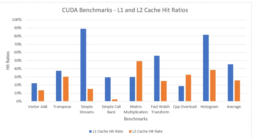
6.2 Results . . . 61
6.2.1 L1 and L2 cache hit ratios . . . 61
6.2.2 MRU and LRU Temporal Locality Results . . . 62
6.2.3 Inter-warp and Intra-warp Locality Results . . . 65
7 Conclusion 70 7.1 Future Work . . . 72
7.1.1 Unified Memory Model . . . 72
7.1.2 Machine Learning Benchmarks on the GPU . . . 72
List of Figures
3.1 Block diagram of the AMD 7970 architecture [14] . . . 16
3.2 Block diagram of the Compute Unit of the AMD 7970 architecture [14] 17 3.3 Block diagram of the NVIDIA Kepler architecture [1] . . . 19
3.4 Kepler GPU Memory Architecture [1] . . . 20
3.5 NVIDIA Kepler Steaming Multi-processor (SM) architecture [1] . . . 21
4.1 Cache Replacement Policies [15] . . . 29
5.1 Cache Memory Hit Ratios for the OpenCL benchmarks . . . 40
5.2 Cache Memory Hit Ratios for the CUDA benchmarks . . . 40
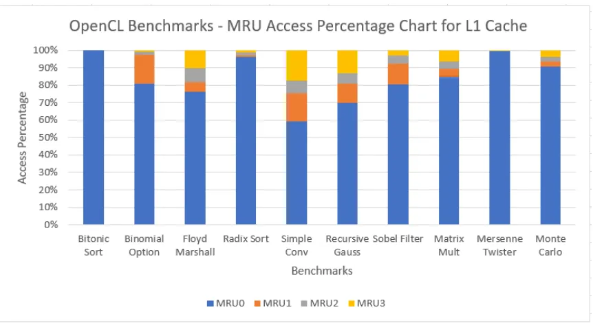
5.3 OpenCL benchmark results for the AMD SI architecture for L1 cache 42 5.4 CUDA benchmark MRU Results for L1 Cache of the NVIDIA Kepler architecture . . . 43
5.5 OpenCL benchmark results for the AMD SI architecture for L2 cache 45 5.6 CUDA benchmark MRU Results for L2 Cache of the NVIDIA Kepler architecture . . . 46
5.7 OpenCL L1 vector and L2 cache intra-warp and inter-warp access per-centages . . . 49
5.8 CUDA L1 vector and L2 cache intra-warp and inter-warp access per-centages . . . 50
5.9 OpenCL L1 vector intra-warp and inter-warp hits and misses . . . 52
5.10 OpenCL L2 intra-warp and inter-warp hits and misses . . . 52
5.11 CUDA L1 intra-warp and inter-warp hits and misses . . . 53
5.12 CUDA L2 intra-warp and inter-warp hits and misses . . . 53
6.1 Machine Learning benchmark results for the NVIDIA Kepler architec-ture for L1 cache . . . 63
6.2 Machine Learning benchmark results for the NVIDIA Kepler architec-ture for L2 cache . . . 64
6.3 L1 and L2 cache inter-warp and intra-warp access percentages for Ma-chine Learning benchmarks . . . 66
LIST OF FIGURES
6.5 L2 intra-warp and inter-warp hits and misses for Machine Learning
benchmarks . . . 67
List of Tables
3.1 Dependency list for the Multi2Sim simulator . . . 13
3.2 Difference in terminology between OpenCL and CUDA . . . 15
3.3 AMD Southern Islands emulated GPU configuration on Multi2Sim [10, 14] . . . 18
3.4 NVIDIA Kepler emulated GPU configuration on Multi2Sim [1, 14] . . 22
5.1 OpenCL Benchmark MRU results for L1 Cache (per module) of the AMD SI architecture . . . 42
5.2 CUDA Benchmark MRU results for L1 Cache of the NVIDIA Kepler architecture . . . 43
5.3 OpenCL Benchmark MRU results for L2 Cache of the AMD SI archi-tecture . . . 45
5.4 CUDA Benchmark MRU results for L2 Cache of the NVIDIA Kepler architecture . . . 46
5.5 Inter-warp and Intra-warp Access Percentages for L1 and L2 cache for OpenCL benchmarks . . . 49
5.6 Inter-warp and Intra-warp Access Percentages for L1 and L2 cache for CUDA benchmarks . . . 50
5.7 MRU Results for the CPU [11] . . . 54
5.8 Comparison of MRU results for the CPU and the GPU [11] . . . 55
5.9 Cache Hit Rates for the CPU [10] . . . 56
5.10 Comparison of Cache Hit Ratios for the CPU and the GPU . . . 57
6.1 Defined Machine Learning algorithms in CUDA . . . 59
6.2 L1 and L2 Hit Ratios for Machine Learning Benchmarks . . . 61
6.3 MRU Results for the Machine Learning benchmarks on the NVIDIA Kepler architecture for L1 cache . . . 62
6.4 MRU Results for the Machine Learning benchmarks on the NVIDIA Kepler architecture for L2 cache . . . 63
6.5 Inter-warp and Intra-warp Access Percentages for L1 and L2 cache . . 66
Chapter 1
Introduction
Graphic Processing Units (GPUs) are regarded as one of the standards when it comes
to high processing power and parallel execution. As the world advances in technology,
the applications of GPUs range from machine learning and computer vision to general
purpose computing and more. Although the use of GPUs is growing greatly in
indus-try, there is very little knowledge and understanding of GPUs and their relationship
with cache, as well as the communication between a CPU and a GPU.
Data level parallelism is achieved when multiple processors work on the same code
to execute the results in parallel therefore improving the performance. GPUs enabled
programmers to run multiple applications using data level parallelism by executing
multiple threads in parallel. This was done using the defined hardware characteristics,
such that each thread will execute the same kernel functionality. This execution model
is one level higher than the Single Instruction Multiple Data (SIMD) model and is
called Single Instruction Multiple Thread (SIMT). In 2007, NVIDIA launched their
first GPU accelerators with supporting hardware to improve the performance of high
end applications. GPU accelerators are mainly used in heterogeneous multi-processor
systems, where the GPU works in tandem with the CPU to improve or accelerate
performance.
In a heterogeneous multi-processor chip, the CPU and GPU are the two main
CHAPTER 1. INTRODUCTION
off the primary host (CPU). The CPU’s cache memory access patterns are very well
documented, but the same cannot be said about the GPU. There has not been enough
research done in the GPU field to understand how the GPU accesses its cache and to
understand the cache memory access patterns of the GPU.
1.1
Motivation
One of the primary objectives of this research is to understand the GPU cache memory
access patterns and in turn improve the communication between GPU and CPU in a
heterogeneous multi-processor chip. A GPU simulator called Multi2Sim was used to
simulate various benchmarks for two sets of GPU architectures — NVIDIA’s Kepler
and AMD’s Radeon.
The development of GPUs has enabled high data parallelism using multiple, easy
to use, and flexible programming models. Modern GPUs can be used for general
purpose processing and are part of a heterogeneous multi-processor chip along with
the CPU. Modern GPUs offer greater computational power than the CPU and are
used to run applications in parallel taking advantage of the application’s data level
parallelism. GPUs are Single Instruction Multiple Data (SIMD) architectures. This
enables them to offer greater performance with low latency and overhead.
In a heterogeneous multi-processor system, different tasks are assigned to and
handled by different processing cores based on the individual characteristics of the
processor and the task assigned to it. This improves performance and saves power,
effectively using the available resources on the system or chip with an even work load
for the processors.
Understanding the memory access patterns of the GPU can lead to improving the
communication and memory management between the CPU and the GPU. The CPU
cache memory definitions and access patterns have been studied and identified for
CHAPTER 1. INTRODUCTION
of cache hits along the multiple lines for each set of the CPU’s cache. Various CPU
benchmarks were run to identify the temporal locality of lines for each set of CPU
cache. The first MRU line shows a very high percentage of cache hits between 85%
to 95%, depending on the benchmarks being tested. The other 15% to 5% of hits
were then distributed among the other MRU lines. The results showed a very high
percentage of hits on the Most Recently Used (MRU) block or MRU0 line, and this
value was recorded to be 92% on average. This served as a motivation to find the
MRU cache access patterns of the GPU to see if the GPU showed similar results to
those of the CPU.
Studying the GPU cache locality and cache memory access patterns can further
help understand the working of the GPU for specific high-performance benchmarks
like those used for machine learning. Most of the machine learning workloads are
executed using pre-defined libraries or frameworks like Tensorflow. These machine
learning workloads are heavily reliant on a GPU for high data level parallelism and
high computational power. To the best of the author’s knowledge, machine learning
algorithms or workloads have not been tested on a simulator level to understand
how the GPU works with these different workloads and how this impacts its cache
memory. By running some machine learning benchmarks on the Multi2Sim simulator
for the GPU, the GPU cache behavior can be studied for different machine learning
workloads.
This research can also pave the way for a new approach, currently being pursued
by AMD and NVIDIA, called the Unified Memory Model[27] between the CPU and
the GPU. Based on this model, the CPU and GPU share a dedicated unified memory
block located in Dynamic Random Access Memory (DRAM), where the GPU can
CHAPTER 1. INTRODUCTION
1.2
Objective
The main objective of this research is to learn more about the cache memory access
patterns of the GPU. These results will help identify specifics about GPU cache
operations and can be used to improve data exchange between the GPU and the
CPU in a heterogeneous multi-processor chip. Multi2Sim [6] was used to perform a
wide range of simulations on two different GPU architectures. Mult2Sim emulates
the AMD’s Radeon GPU architecture as well as NVIDIA’s Kepler GPU architecture.
A set of OpenCL and CUDA benchmarks was used to test both GPU architectures
for different workloads.
The first objective was to setup the Multi2Sim simulator on an Ubuntu VM with
all the required dependencies. The simulator was compiled to run the OpenCL and
CUDA benchmarks to test the working of the GPU. To modify the GPU emulator
code defined in the Mult2Sim simulator, first there was a need to understand how the
AMD and NVIDIA GPUs were defined in hardware and how they were emulated in
code on the simulator. After understanding the architectural code and the memory
code, three metrics were defined to analyze GPU cache behavior: cache hit ratios,
MRU temporal locality and inter-warp/intra-warp locality.
The caching policy was studied to add specific cache counters to keep track of
the most recently used (MRU) and least recently used (LRU) blocks in the GPU
cache. A set of MRU and LRU counters were implemented to study the temporal
locality of the the GPU cache. These MRU counters determine the number of cache
accesses made for each MRU line in a multi-way set associative cache. In the GPU
architecture, L1 and L2 cache blocks were defined using different set associativity.
This associativity determined how many ways or lines were used to split the cache.
For example, if L1 cache was defined a 4-way set associative cache, then each set
CHAPTER 1. INTRODUCTION
MRU4 would represent the least recently used line. The caching policy uses these
multiple lines to add, replace, and remove blocks of memory for each set in cache.
The MRU counters were updated during the GPU execution every time a block got
accessed in cache at that very location on the MRU line. The respective MRU line
counter was incremented. These MRU counters were used to record the temporal
locality of the GPU in L1 and L2 cache. These GPU MRU results were compared
to those of the CPU to see if the GPU showed similar values and access patterns to
those of the CPU.
A set of inter-warp and intra-warp cache counters were implemented to understand
the cache locality for different sets of workloads for the defined GPU architectures.
The intra-warp access counters represent the accesses made within each warp while
the inter-warp access counters represent the accesses made across various warps in the
overall GPU architecture. This set of counters can help analyze the cache memory
access patterns of a GPU. The L1 and L2 intra hits were defined as the number of L1
and L2 data cache hits that resulted from intra-warp locality, respectively. Contrarily,
the L1 and L2 inter hits were the data cache hits that resulted from inter-warp locality.
This helped understand the cache locality of the GPU architecture for different sets
of workloads.
Furthermore, some machine learning benchmarks were defined in CUDA and
tested on the GPU architecture to analyze how the GPU reacts to different
ma-chine learning workloads. These benchmarks were defined using math algorithms
that are most commonly used by Convolution Neural Networks (CNN) and Deep
Neural Networks (DNN). The cache hit ratios, MRU temporal locality and the
inter-warp/ intra-warp locality were recorded and compared against the general purpose
Chapter 2
Background
2.1
Simulators
A large portion of the work in this thesis focused on setting up the right GPU
simu-lator. GPGPU Sim [1, 2] was the most popular simulator a few years ago, and most
of the research in the GPU field was performed using this simulator. The advantages
of this simulator were that it was easy, convenient and had all the latest GPU
archi-tectures modeled to replicate GPUs in hardware, at that time. But over the years,
this simulator has not been updated, and this results in many compatibility issues in
terms of the latest versions of CUDA, OpenCL, GCC compilers and Python. This
meant that this simulator could not be used to perform experiments for the latest
GPU architectures, to study recent technology trends. This GPGPU simulator
re-cently merged with Gem5 [3], but the some of the dependencies still have not been
updated. Hence neither simulator (GPGPU Sim or Gem5-gpu) was chosen for these
experiments.
Barra [1, 4] and Ocelot [1, 5] are some of the other GPU simulators that were
considered for this research. The drawback of Barra is that it runs CUDA applications
and benchmarks for NVIDIA GPUs only and does not have the capability to run any
OpenCL applications and benchmarks for the AMD series of GPUs. In addition to
CHAPTER 2. BACKGROUND
Instruction Set Architecture (ISA) and not on a Parallel Thread Execution (PTX)
level. Unlike Barra, Ocelot supports both CUDA and OpenCL benchmark on a ISA
and PTX level. Since Ocelot has not been maintained and updated to the latest SDK,
GCC, and CUDA releases and hence was not chosen for this research.
Multi2Sim [1, 6] was chosen as the main simulator for this research as it was the
most up-to-date simulator with the latest dependencies and accurate functionality.
Multi2Sim is easy to setup and use, and it is very well documented and supported,
being one of the newer open source simulators out there. Older versions of Multi2Sim
supported only CPU architecture simulations. But recent simulator released have
helped incorporate GPU architecture emulation and simulation for AMD’s Radeon
Southern Islands series and for NVIDIA’s Kepler GPU series. This is another
advan-tage as this simulator can be used to run both OpenCL and CUDA benchmarks to
test the AMD Radeon and NVIDIA Kepler GPU architectures.
2.2
Related Work
In this new generation of high performance computing, the GPUs have taken up a
new distinction in terms of processing power using parallel thread execution. The
technology has a come a long way since the initial release of the GPU in terms of its
architecture and how it works communicates with the CPU.
Lee et al. [7] proposed a method to improve GPU performance by updating
the warp scheduling policy within a GPU architecture. This method also used a
simulator and tested the scheduling policies of the GPU, like the round-robin and
greedy instruction issue scheduling policies and patterns. Most of the related research
in this field had focused on static scheduling methods for all workloads, and this
was the first time a dynamic or adaptive instruction issue scheduling policy was
suggested. The proposed method was called instruction-issue pattern based adaptive
CHAPTER 2. BACKGROUND
round-robin scheduler based on the type of workload being run on the GPU. Various
sets of benchmarks were run to simulate large diverse workloads on an NVIDIA
GPU using CUDA. The proposed adaptive warp scheduling method was observed to
be optimal than the static greedy or round-robin scheduling methods. This paper
accurately described the use of a GPU simulator for results and defined the GPU
modifications well in terms of the GPU architecture. This paper served as a baseline
for the use of a GPU simulator for a similar research in the GPU field, but this time
to analyze the memory access patterns of a GPU. This paper also presented GPU
results for warp locality mainly, inter-warp and intra-warp statistics in L1 and L2
cache. This helped in understanding the warp locality for different sets of workloads
for both the Greedy, Round-Robin scheduling policies and iPAWS (as suggested by
the paper).
Mei et al. [8] talk about the GPU memory hierarchy through micro-benchmarking.
This paper proposes a new micro-benchmarking approach to test the GPU cache
memory components for three NVIDIA GPU models: Kepler, Fermi and Maxwell.
The memory components studied are data cache, texture cache, and translation
look-aside buffer (TLB). This paper goes on to introduce the proposed micro-benchmarking
approach to study the memory access patterns of the GPU which are comprised of
cache memory units with the Least Recently used (LRU) caching policy. The memory
access patterns of the GPU and the memory statistics, like number of accesses, number
of hits, number of misses, hit-ratio, etc. were recorded for the new proposed method
of fine grained benchmarking method. The proposed method proved to enhance the
memory capability and capacity for all three generations of the NVIDIA GPUs, more
so for Kepler and Maxwell than Fermi. Furthermore, it enhanced the performance
of the GPU by reducing the latency for shared memory of the GPU caused due to
bank conflicts. Some of the drawbacks or limitations of this approach included low
CHAPTER 2. BACKGROUND
Johnstone et al. [9] talk about the bandwidth requirements of the GPU cores
to determine the appropriate choice of an interconnect between the GPU and CPU
in a heterogeneous multi-core chip. This paper completely focused on running GPU
simulations for different benchmarks and workloads using GPGPU simulator. The
interconnect properties were found to be dependent on the performance of the GPU,
and how the bandwidth affected the GPU performance. The GPU architectures and
the use of GPGPU simulator were the main takeaways from this paper in relation to
this research area.
Choo et al. [10] talk about analyzing and optimizing GPU cache memory
perfor-mance for different computational workloads using Multi2Sim. This paper used the
AMD Southern Islands (SI) GPU architecture defined on MultiSim to run various
computational workloads and observe the L1 and L2 cache hit rates and behavior.
The L1 and L2 cache hit ratios were compared for the CPU and the GPU. The CPU
showed much higher cache hit ratios than the GPU as expected, as the CPU focuses
more on the memory hierarchy during execution to increase performance. On the
other hand, the GPU relies more on parallel execution to process larger workloads
such that the same set of instructions can be executed across multiple threads to
increase productivity and performance. Since this paper used Multi2Sim, it was used
as a reference point for any AMD SI GPU simulations performed during this
the-sis. The cache hit ratios recorded from this thesis were also compared to the results
recorded from this paper for reference. There was no research in terms of caching
policies or identifying the most recently used blocks in cache memory. This paper
completely focuses on improving the GPU memory performance by proposing two
methods: shared L1 vector data cache and clustered work-group scheduling. Both of
these methods were executed for different workloads, and the performance
improve-ments were recorded.
CHAPTER 2. BACKGROUND
studied and identified for various releases of CPUs [11, 12, 13]. Savaldor Petit et
al. [11] investigated the temporal locality of a multi-way set associative cache by
recording the percentage of cache hits along the multiple lines for each set of the
CPU’s cache. This helped analyze the power consumption and performance of the
CPU for the different cache lines using the current caching policies. A new drowsy
cache policy was proposed to demonstrate a good balance between performance and
power consumption. The experiments were performed using the HotLeakage simulator
and the Spec2000 benchmark suite for CPUs. This drowsy cache policy was then
compared to two existing caching policies, Most Recently Used On (MRO) and Two
Most Recently Used On (TMRO), to compare the performance and power statistics.
This research involved going through each Most Recently Used (MRU) block or line in
cache and the power values, and hit percentages were recorded for each line. Various
CPU benchmarks were run to identify the temporal locality of lines for each set of
CPU cache. The first MRU line shows a very high percentage of cache hits between
85% to 95%, depending on the benchmarks being tested. The other 15% to 5% of
hits were then distributed among the other MRU lines. The results showed a very
high percentage of hits on the Most Recently Used (MRU) block or MRU0 line, and
this value was recorded to be 92% on average. This paper serves as a good reference
point for the MRU cache access patterns for the CPU. This served as a motivation
to find the MRU cache access patterns of the GPU to see if the GPU showed similar
results to the CPU results recorded by this paper.
Kumar et al. [12] talk about the modern CPU cache memory hierarchy and
perform cache analysis for various cache replacement policies in CPU cache memory.
The latest generations of processors were compared to find the different sets of factors
that affect the performance and utilization of cache memory. Furthermore, the cache
replacement policies were studied and analyzed using performance analysis. Banday
CHAPTER 2. BACKGROUND
Most of the latest processors were compared based on cache hierarchy, organization,
performance, cache access patterns and cache replacement policies. The CPU’s cache
memory access patterns and functionality are known and have been studied for years,
Chapter 3
Multi2Sim
Multi2Sim is a well known and documented research simulator. The simulator was
recently updated to include certain GPU architectures. Furthermore, Multi2Sim is
regarded as the most up to date open source simulator that works with the latest
versions of CUDA, OpenCL, Python, and GCC.
As stated previously, the two main GPU architectures that Multi2Sim can
simu-late are AMD’s Radeon Southern Islands and NVIDIA’s Kepler GPU architectures.
Both GPU architectures are approximately two generations behind the current
in-dustry standard, as is the case with most of the CPU and GPU simulators. However,
they can be modified to add any current or new architectures at the simulation level
using newer releases. Both AMD Radeon and NVIDIA Kepler represent really strong
GPUs that are used for a wide variety of applications like parallel and high
perfor-mance computing. They are commonly used in machine learning and computer vision
applications, mainly using libraries and frameworks like Tensorflow. AMD’s SI GPU
architecture used the OpenCL libraries and framework while NVIDIA’s Kepler GPU
architecture used CUDA libraries.
Multi2Sim emulates GPU architectures in software and enables the user to run
a variety of benchmarks on the CPU itself as though the experiments were being
run on a GPU. This enables the user to make architectural changes to the defined
CHAPTER 3. MULTI2SIM
Table 3.1: Dependency list for the Multi2Sim simulator
Dependency Version
Operating System Ubuntu (14.04 preferred)
CUDA CUDA version 6.5 (preferred) or higher
Python Python2 and Python3
GCC GCC version 4.8.2 or higher
in the GPU emulator code, the Multi2Sim framework is recompiled to reflect those
changes, and a new executable is generated to run simulations. Multi2Sim supports
multiple CPU and GPU benchmarks that help test the architectures for different
workloads. Spec2000 is the most commonly used CPU benchmark suite. Contrarily,
AMD SDK 2.5 [21] CUDA SDK [22] are the commonly used GPU benchmark suites.
Both OpenCL and CUDA benchmarks display two sections, one for the CPU and one
for the GPU. Both the CPU and GPU sections are simulated on the respective CPU
and GPU architectures implemented in software by Multi2Sim.
3.1
Setting up the simulator on an Ubuntu OS
The open source Multi2Sim simulator code was downloaded from the official M2Sim
github repository and was setup on a 64 bit Ubuntu 14.04 operating system. Although
Ubuntu is the primary OS supported by Multi2Sim, the 14.04 version is the optimal
Ubuntu version as the simulator was tried and tested on this version during the
developmental phase. This does not limit the Multi2Sim to only the 14.04 version.
Systems with newer Ubuntu versions can also be used to setup this simulator.
Table 3.1 shows the major dependencies of the Multi2Sim simulator. These
spe-cific packages and versions had been tested during the developmental stages of the
CHAPTER 3. MULTI2SIM
Helper tools were used to download and add the installation scripts for the
sim-ulator. After running the configure and make install commands, Multi2Sim was successfully built, and them2s executable was generated in the dedicated Multi2Sim home directory. The m2s executable was used to run various simulations on the defined CPU and GPU architecture models. All the commands supported by the
simulator were listed by running the command m2s –help. Listing 3.1 shows all the bash commands that were used to configure and install Multi2Sim.
1
2 # I n s t a l l i n g any d e p e n d e n c i e s − i f r e q u i r e d
3 $ s u d o yum i n s t a l l d e v t o o l s e t−2
4 $ s c l e n a b l e d e v t o o l s e t−2 b a s h
5
6 # Bash Commands t o i n s t a l l M u l t i 2 S i m
7 $ l i b t o o l i z e
8 $ a c l o c a l
9 $ a u t o c o n f
10 $ automake −−add−m i s s i n g
11
12 $ cd ˜ M u l t i 2 S i m H o m e D i r e c t o r y
13 $ . / c o n f i g u r e −−p r e f i x =/home/ ypn4262 / t o o l s / m u l t i 2 s i m / 5 . 0 /
14
15 # C o m p i l i n g a l l t h e s i m u l a t o r s o u r c e f i l e s and g e n e r a t i n g t h e m2s e x e c u t a b l e
16 $ make−j 4
17 $ make i n s t a l l
18
19 # U s i n g t h e h e l p command t o f i n d a l l t h e a v a i l a b l e commands f o r M u l t i 2 S i m
20 $ m2s−h e l p
21 $ . / t o o l s / m u l t i 2 s i m / 5 . 0 / b i n /m2s−−h e l p
Listing 3.1: Bash commands to setup Multi2Sim
3.2
AMD Southern Islands (Radeon) GPU Architecture
AMD’s Radeon series of GPUs are the closest competitors to NVIDIA’s GeForce
series of GPUs. AMD’s Southern Islands family of HD GPUs consists of the Radeon
HD 7000 series of GPUs. The Southern Islands architecture defined by Multi2Sim
consists of Radeon HD 7770, 7850, 7870 and 7970 architectures. The default and most
commonly used Southern Islands architecture is Radeon HD 7970. This architecture
CHAPTER 3. MULTI2SIM
Table 3.2: Difference in terminology between OpenCL and CUDA
OpenCL CUDA
Compute Unit (CU) Streaming Multiprocessor (SM)
Compute Element CUDA Core
Work-item Thread
Wavefront (64 work-items) Warp (32 threads)
Wavefront pool Warp pool
Work-group Thread block
Local memory Shared memory
Private memory Registers
The AMD SI GPU architecture used an OpenCL Application Programming
In-terface (API) platform which serves as a parallel to the CUDA platform of NVIDIA’s
GPUs. In the OpenCL implementation, the GPU is defined with Compute Unit (CU)
which serves as the CUDA equivalent of NVIDIA’s Streaming Multiprocessor (SM).
Furthermore, OpenCL APIs use work items, wavefront, and wavefront pools which
serve as the CUDA equivalent of NVIDIA’s threads, warps, and warp pools (or thread
blocks) respectively. Table 3.2 shows the difference in terminology between OpenCL
and CUDA.
Figure 3.1 shows a block diagram of the AMD Radeon 7970 architecture from
the AMD Southern Islands GPU family. The Radeon 7970 architecture has three
main parts, compute devices, compute units and SIMD lanes. Figure 3.1 (a) shows
the block diagram of a compute device. This specific architecture is defined using a
thread dispatcher and scheduler with 32 compute units. The ultra-thread dispatcher
is responsible for scheduling work groups and assigning them to the available Compute
Units. The Compute Units interact directly with global memory, which is comprised
of cache memory and main memory. This global memory block can be accessed by
the entire collection of Compute Units in the ND-Range [14].
CHAPTER 3. MULTI2SIM
Figure 3.1: Block diagram of the AMD 7970 architecture [14]
unit has 4 SIMD execution units, each having 16 SIMD lanes for parallel work-item
execution. These SIMD units are free to interact directly with local memory. The
SIMD lanes allow parallel work-item execution, such that the same set of instructions
is executed across multiple work-items. A wavefront consisting of 64 work-items is
created within each work group and is assigned to a specific SIMD unit for execution.
Each of the 16 SIMD lanes of the Compute Unit is executes four work-items per
wavefront. The local memory block allows the work-items to share information during
execution [14].
Figure 3.1 (c) represents a single SIMD lane which shows how an ALU interacts
with the register file. The ALU is comprised of functional units to process integer
and floating-point values. The register file is responsible for each work-item’s private
memory [14].
Figure 3.2 shows a block diagram of the Compute Unit of the AMD Radeon 7970
GPU architecture. The figure shows the modular structure of the Compute Unit
comprising of a Scalar Unit, Vector Memory Unit, Branch Unit, Local Data Share
Unit (LDS) unit, and 4 SIMD units for parallel execution. During execution, multiple
work-groups are assigned to each compute unit. These work-groups are further split
into wavefronts (comprised of 64 work-items), and the wavefronts are executed
simul-taneously for each instruction. The front-end of the Compute Unit fetches and reads
CHAPTER 3. MULTI2SIM
Figure 3.2: Block diagram of the Compute Unit of the AMD 7970 architecture [14]
to the functional units for execution. The Scalar Unit executes scalar arithmetic
and scalar memory instructions. The Vector Memory Unit handles all vector global
memory instructions. The Local Data Share Unit (LDS) handles the local memory
instructions. The Branch Unit (BRU) handles all the branch instructions for control
flow. Each of the functional units (SIMD units) interacts with either global or local
memory and executes vector arithmetic and logic instructions [14].
Table 3.3 shows the hardware configuration of the AMD Radeon 7970 GPU series
that was replicated by the AMD SI GPU model in Multi2Sim [10, 14]. L1 cache and
L2 cache were defined as 4-way and 16-way set associative caches, respectively. The
L1 cache was split between L1 scalar cache and L1 vector cache. The L1 scalar cache
was responsible for all the L1 scalar instructions that got fetched and executed only
once for the entire wavefront. Most of the constant data values were stored here. The
L1 vector cache was responsible for all the vector instructions that got fetched for
the whole wavefront but got executed multiple times for each of the 64 work-items in
that wavefront for parallel execution. The L1 vector cache was the primary focus for
CHAPTER 3. MULTI2SIM
Table 3.3: AMD Southern Islands emulated GPU configuration on Multi2Sim [10, 14]
Configuration Value
Computational
Frequency 1000 Hz
Number of Compute Units 32 Number of SIMD lanes 16 Max Number of Wavefront Pools 4
Max Wavefronts per Pool 10
L1 Vector Cache
Number of L1 Cache Modules 32 Associativity / Number of Ways 4
Number of Sets 64
L1 Block Size 64 B
Total L1 Cache Size 512 KB
L1 Scalar Cache
Number of L1 Cache Modules 8 Associativity / Number of Ways 4
Number of Sets 64
L1 Block Size 64 B
Total L1 Cache Size 128 KB
L2 Cache
Number of L2 Cache Modules 6 Associativity / Number of Ways 16
Number of Sets 128
L2 Block Size 64 B
Total L2 Cache Size 768 KB
of the 32 compute units is directly mapped to a single L1 cache module. L2 cache
has 6 memory modules that are shared by all of the 32 compute units. The L2 cache
had a higher set associativity than L1 cache and was larger than L1 cache in terms
CHAPTER 3. MULTI2SIM
Figure 3.3: Block diagram of the NVIDIA Kepler architecture [1]
3.3
NVIDIA Kepler GPU Architecture
NVIDIA is the leader in the GPU market with its latest generation GeForce GPU
series. The NVIDIA Kepler GPU architecture was the sole NVIDIA architecture
available on Multi2Sim, but future updates may result in other GPU models. The
Kepler architecture comprises of the GeForce 6000 series and the GeForce 7000 series
GPUs.
Figure 3.3 shows a block diagram of the NVIDIA Kepler architecture from the
Kepler series of GPUs. Part (a) shows the block diagram of the SIMD execution
pipeline of the GPU. The SIMD pipeline consists of the front end, a register file, 32
SIMD lanes followed by an execution buffer. Part (b) shows a block diagram of the
Branch Unit (BRU) in the GPU architecture. The BRU describes how the opcode is
fetched from the dispatch buffer and sent to the execution unit. Moreover, the data
are written to the register file using the write buffer. Part (c) shows the Load and
Store Unit (LSU) of the GPU architecture. The LSU controls how the GPU interacts
with its different memory units like cache, shared memory, global memory, and local
memory. The LSU unit is used by the Streaming Multiprocessor (SM) to interact
with the GPU’s memory units, and data are either written to or read from these
CHAPTER 3. MULTI2SIM
Figure 3.4: Kepler GPU Memory Architecture [1]
Figure 3.4 shows the top level block diagram of the Kepler GPU architecture.
The GigaThread Engine interacts with the SMs which in turn interact with global
memory. There are a total of 14 SMs defined in the Kepler architecture on the
Multi2Sim and each SM has a dedicated L1 cache module assigned to it. The L2 cache
modules are shared between multiple SMs. Finally, the entire memory architecture
is supported using interconnects and memory controllers. The GigaThread engine
is responsible for storing and assigning the thread blocks to the defined SMs. The
block and grid dimensions are defined in the GigaThread Engine. The engine is in
charge of assigning thread blocks to available SMs for execution. The thread blocks
then get passed on to the SM where they get executed for the fetched instruction
opcode. Based on available resources, multiple thread blocks may be assigned to the
same SM. The Kepler architecture is defined using CUDA, which specifies a thread
as set of instructions to be executed. Multiple threads can be executed in parallel
using the Single Instruction Multiple Data (SIMD) pipeline which enables high data
level parallelism. In CUDA, a group of threads is defined as a thread block, where
all the threads in that thread block execute the same set of instructions in parallel.
A group of 32 threads is defined as a warp, and a thread block is further comprised
CHAPTER 3. MULTI2SIM
Figure 3.5: NVIDIA Kepler Steaming Multi-processor (SM) architecture [1]
architecture defines 4 warp schedulers, thus enabling 4 warps to be scheduled and
processed at the same time [8].
Figure 3.5 shows the block diagram of the Streaming Multiprocessor (SM) in the
Kepler architecture. Each SM is comprised of various functional units like the Single
Precision Unit (SPU), the Branch Unit (BRU), the Double Precision Unit (DPU),
the Integer Math Unit (IMU), the Special Functional Unit (SFU), and the Load and
Store Unit (LSU).
Table 3.4 shows the hardware configuration of the NVIDIA Tesla K20X GPU [17,
18] that was matched by the NVIDIA Kepler GPU architecture on Multi2Sim.
Similar to the AMD GPU architecture, NVIDIA’S Kepler architecture also defines
L1 caches and L2 caches as 4-way and 16-way set associative cache blocks, respectively.
L1 cache had 14 memory modules such that each of the 14 Streaming Multiprocessors
CHAPTER 3. MULTI2SIM
Table 3.4: NVIDIA Kepler emulated GPU configuration on Multi2Sim [1, 14]
Configuration Value
Computational
Frequency 732 Hz
Number of SMs 14
Number of SIMD lanes 32
Warp Size 32
Max Warps per SM 64
Max Threads per SM 2048
L1 Cache
Number of L1 Cache Modules 14 Associativity / Number of Ways 4
Number of Sets 32
L1 Block Size 128 B
Total L1 Cache Size 16 KB
L2 Cache
Number of L2 Cache Modules 6 Associativity / Number of Ways 16
Number of Sets 32
L2 Block Size 128 B
Total L2 Cache Size 1536 KB
memory modules which are shared by all of the 14 SMs.
The AMD SI and NVIDIA Kepler GPU architectures were both linked to Multi2Sim’s
common memory model. Initially, the NVIDIA Kepler architecture was not connected
to any memory module, as the common memory module defined in Multi2Sim was
based on the AMD GPU’s memory hierarchy. After a discussion with the Multi2Sim
Developers team, there was consensus that the memory model could be connected to
the NVIDIA Kepler GPU architecture to show accurate functionality. Multi2Sim’s
memory module was then connected to the NVIDIA Kepler GPU architecture in the
LSU unit of the SM definition. The LSU unit was responsible for all memory
ac-cesses. Since both GPU architectures used a common memory model, the results
were consistent and easy to compare.
Listings 3.2 and 3.3 show the UNIX commands used to compile and run OpenCL
CHAPTER 3. MULTI2SIM
1 #C o m p i l i n g t h e Benchmarks
2
3 cd Benchmarks Home Dir
4 cd M a t r i x M u l t i p l i c a t i o n #( o r any o t h e r benchmark )
5 vim M a k e F i l e #( To u p d a t e t h e M a k e F i l e and t h e M u l t i 2 S i m d i r e c t o r y )
6 #( And l i n k i n g t h e OpenCL and CUDA l i b r a r i e s )
7 make #( To c o m p i l e t h e benchmark )
Listing 3.2: Compiling the OpenCL and CUDA benchmarks
1 #Running AMD SDK 2 . 5 Benchmark ( forAMD S o u t h e r n I s l a n d )
2
3 <m u l t i 2 s i m b i n a r y><benchmark h o s t program> l o a d <benchmark GPU b i n a r y>
4
5 . / m2s−−s i−r e p o r t r e p o r t . t x t −−mem−r e p o r t m e m r e p o r t . t x t −−s i−s i m d e t a i l e d
6 m2s−bench−amdsdk−2.5−m a s t e r / M a t r i x M u l t i p l i c a t i o n / M a t r i x M u l t i p l i c a t i o n −−l o a d
7 m2s−bench−amdsdk−2.5−m a s t e r / M a t r i x M u l t i p l i c a t i o n / M a t r i x M u l t i p l i c a t i o n K e r n e l s . b i n −q
8
9
10 #Running CUDA SDK 2 . 5 Benchmark ( f o r NVIDIA K e p l e r )
11
12 <m u l t i 2 s i m b i n a r y> <benchmark GPU b i n a r y>
13
14 e x p o r t LD LIBRARY PATH=/home/ t o o l s / m u l t i 2 s i m / 5 . 0 / l i b
15
16 . / m2s−−k p l−r e p o r t k p l r e p o r t . t x t −−mem−r e p o r t k p l m e m r e p o r t . t x t −−k p l−s i m d e t a i l e d
17 /home/ ypn4262 / T h e s i s / m2sim / b e n c h m a r k s /m2s−bench−c u d a s d k−6.5−m a s t e r / VectorADD / v e c t o r A d d m 2 s
Chapter 4
Analyzing Cache Memory Access Patterns
The objective of this research is to analyze cache memory access patterns for GPU
architectures. In particular, the three metrics include cache hit ratios, Most Recently
Used (MRU) and Least Recently Used (LRU) cache access counters, and finally data
cache accesses for intra-warp and inter-warp locality for different workloads.
The L1 and L2 cache statistics and hit ratios were compared for a variety of
bench-marks for both AMD SI and NVIDIA Kepler GPU models. The data cache hit ratios
varied based on the benchmark being tested and depended greatly on the benchmarks
size. Each benchmark was run for multiple input sizes to find the optimal cache hit
ratio. All cache hit ratios were compared for the all benchmarks to understand the
cache performance of both AMD SI and NVIDIA Kepler GPU architectures for the
tested workloads.
The MRU and LRU counters recorded the most and least recently used blocks in
each set for L1 and L2 cache respectively. The results for each set were combined
to generate cache access percentages for each MRU line in cache. The cache access
percentages for different MRU lines were compared and analyzed to find GPU cache
memory trends for a variety of benchmarks. The GPU results were compared against
the CPU as a reference.
The L1 and L2 data cache accesses were studied for intra-warp and inter-warp
CHAPTER 4. ANALYZING CACHE MEMORY ACCESS PATTERNS
the accessing threads belong to the same warp. Intra-warp accesses represent the
accesses made in data cache where the accessing threads do not belong to the same
warp, but belong to different warps within the warp-pool. The inter-warp and
intra-warp results varied based on the workload characteristics. The cache statistics were
recorded and analyzed for OpenCL and CUDA benchmarks for inter-warp and
intra-warp localities.
4.1
L1 and L2 Cache Hit Ratios
4.1.1 AMD Southern Islands
The hardware configuration defined in Chapter 3 demonstrates the AMD Southern
Islands GPU architecture model on Multi2Sim. This model replicates the AMD
Radeon HD 7970 GPUs series. The AMD Southern Islands GPU model uses a 4-way
set associative L1 cache and a 16-way set associative L2 cache. The L1 cache consists
of two sections, L1 scalar cache and L1 vector cache. L1 scalar cache has a total of
8 defined memory modules, such that each module maps to four compute units. L1
vector cache has a total of 32 defined memory modules, such that each module maps
to a single compute unit. Contrarily, L2 cache does not have any scalar or vector
differentiation. L2 cache consists of 6 cache memory modules which are shared across
all 32 compute units during execution.
Multi2Sim’s pre-defined memory counters were used to find the memory
statis-tics for the entire memory model. These memory statisstatis-tics were recorded for cache
memory, global memory and local memory. The memory statistics included Accesses,
Evictions, Retrieved Accesses, Hits, Misses, and Hit Ratios for each and every
mem-ory module defined in cache. All these statistics across various memmem-ory modules for
the specific type of cache (L1 or L2) were compared. The same set of AMD SDK
CHAPTER 4. ANALYZING CACHE MEMORY ACCESS PATTERNS
cache, L1 vector cache and L2 cache. All the results were tabulated, graphed and
compared to find common trends of cache memory using the defined AMD SI GPU
model on Multi2Sim.
4.1.2 NVIDIA Kepler
Similarly, the L1 and L2 cache statistics were recorded for the NVIDIA Kepler GPU
model on Multi2Sim. Pertaining to the hardware configurations mentioned in Chapter
3 for the Kepler GPU model, the L1 and L2 cache definitions were noted. The
NVIDIA Kepler GPU model did not differentiate the L1 cache as scalar or vector
cache, as the AMD SI GPU model did. The Kepler model defined the L1 cache as
unified cache modules. The Kepler GPU model used a 4-way set associative L1 cache
and a 16-way set associative L2 cache, similar to the AMD SI model. L1 vector cache
has a total of 14 defined memory modules, such that each L1 cache module maps to
a single SM (as the Kepler architecture used 14 SMs). L2 cache consists of 6 cache
memory modules, and these are shared across multiple SMs during execution.
The memory statistics for various CUDA SDK benchmarks were recorded for the
NVIDIA Kepler GPU architecture. The L1/L2 cache hit ratios and memory statistics
were tabulated, graphed and analyzed. The results from the CUDA benchmarks and
OpenCL benchmarks were compared to understand which model worked better with
CHAPTER 4. ANALYZING CACHE MEMORY ACCESS PATTERNS
4.2
MRU and LRU Cache Counters for Temporal Locality
The simulator, timing and memory code for both AMD SI and NVIDIA Kepler GPU
architectures was studied to learn how the memory hierarchy was used in each GPU
architecture. As explained in Chapter 3, the AMD GPU architecture used an OpenCL
API platform while the NVIDIA Kepler GPU architecture used a CUDA API
plat-form.
The Compute Unit (for OpenCL) or the Streaming Multiprocessor (for CUDA) is
the main processing unit of the GPU that executes the defined kernels. Both GPU
models use Multi2Sim’s memory model to load and store data. Specific memory units
are defined in the GPU architectures on Multi2Sim, and these units are responsible for
performing all memory load and store operations for the respective GPU architecture.
This memory unit is called the Vector Memory Unit in AMD’s SI model and Load
and Store (LSU) unit in NVIDIA’s Kepler model respectively.
The memory model was studied to find the cache memory implementation. First,
the pre-defined sets and blocks in cache were modified to include set and block
coun-ters within their respective modular designs. These councoun-ters were incremented every
time the cache block was accessed. Additionally, the cache code was examined to find
the defined caching policies. The cache block used three cache replacement policies:
Random, First In First Out (FIFO) and Least Recently Used (LRU). These cache
replacement policies signify how the list of blocks are replaced in memory.
The Random replacement policy replaces blocks of memory at random when a
new block is added to cache. Each set uses a list to store all the existing blocks in
that respective set. This list of blocks is created during initialization. The new block
replaces the old block at the exact same position in the list of blocks in cache. The
FIFO Replacement policy replaces the blocks in memory using the First In First Out
CHAPTER 4. ANALYZING CACHE MEMORY ACCESS PATTERNS
one to be replaced. The new block replaces the old block at the same position in the
list but with its new time stamp to indicate that it is the most recently added block.
The Least Recently Used (LRU) replacement policy works by removing the least
recently used block from cache memory when the cache is full, and replaces that
block with the new entry. Each set in cache uses its own LRU list, which is a list or
collection of blocks for that respective set in cache. This LRU list is used only for the
Replacement LRU caching policy. The Replacement LRU policy is the most broadly
used replacement policy. Unlike the generic list of blocks used for Random and FIFO
replacement policies, this LRU list organizes the blocks from Most Recently Used
(MRU) to Least Recently Used (LRU) blocks. The LRU list keeps track of the blocks
in cache memory and updates the position of the blocks based on the most recent
cache accesses made. The new block replaces the old block at the same position of
the LRU list. The new block is then removed and added to the front of the LRU list
to indicate that it is the most recently used block in cache. For example, if the LRU
list is organized to accommodate Blocks 1, 2 and 3 (in that order), when the cache
is full and Block3 is the least recently used block in cache, then Block3 is replaced
in the list with the new entry. The new block is placed in the same position as the
replaced block in the LRU list. That new block node is then removed from the list
and is added to the head of the LRU list indicating that Block3 is the most recently
used block and is stored in the first MRU line. The LRU list is ordered from most
recently used blocks to least recently used blocks in cache memory, for each set in
cache. Figure 4.1 shows the three cache replacement policies implemented in the
memory model and their working.
Cache specific counters were defined in the memory hierarchy to keep track of the
Most Recently Used (MRU) and Least Recently Used (LRU) lines in cache memory.
This helped identify the temporal locality of GPU cache and identify certain memory
CHAPTER 4. ANALYZING CACHE MEMORY ACCESS PATTERNS
Figure 4.1: Cache Replacement Policies [15]
as the name signifies, and helped identify the accesses made to the most recently used
and least recently used lines in cache memory. These MRU and LRU counters were
defined for both L1 and L2 cache blocks.
A new LRU counter list was created to replicate the LRU caching list used by
each set in cache. The list was defined in the architecture of the cache itself, such
that it could be updated every time the LRU caching list was updated by the LRU
cache replacement policy. As soon as a cache access was made to a specific block
in cache memory, that block’s index in the LRU caching list was obtained and the
block’s internal counter was incremented. The LRU counter list was then incremented
at the same index to show that the block at that index was accessed. The defined
LRU caching policy protocol identified the block being accessed and then removed
the block node from the LRU caching list placing it at the head of the list. This
CHAPTER 4. ANALYZING CACHE MEMORY ACCESS PATTERNS
last block was the least recently used block. The next time that block was accessed
in cache, the LRU list would increment the counter at the block’s new index thus
replicating the defined functionality.
The same process was repeated for every cache access made, and the LRU counters
(at the respective block indices) were incremented every time a block was accessed
based on the initial position of the block in the LRU caching list. This meant that
the original index of the block was used to show which cache line was accessed in
terms of most recently used down to least recently used.
Listing 4.1 shows the MRU counter implementation in cache. Listing 4.2 shows
how the MRU counters were incremented and updated based on the original index of
the accessed block. This was done in correlation with the LRU caching policy. The
AccessBlock() function defined in the Cache.cc file was modified. Listing 4.3 shows
a small portion of code from the file SystemEvents.cc. The code is used to call the
AccessBlock() function every time a cache access is made. The memory module’s
CHAPTER 4. ANALYZING CACHE MEMORY ACCESS PATTERNS
1 c l a s s S e t
2 {
3 // Only Cache n e e d s t o i n i t i a l i z e f i e l d s
4 f r i e n d c l a s s Cache ;
5
6 // L i s t o f b l o c k s i n LRU o r d e r − Pre−d e f i n e d and u s e d by t h e LRU c a c h i n g p o l i c y
7 m i s c : : L i s t<B l o c k> l r u l i s t ;
8
9 // P o s i t i o n i n Cache : : b l o c k s w h e r e t h e b l o c k s s t a r t f o r t h i s s e t
10 B l o c k ∗b l o c k s ;
11
12 // C r e a t i n g a l i s t o f MRU/LRU c o u n t e r s
13 i n t∗ l r u c o u n t e r s ;
14
15
16 v o i d i n i t l r u c o u n t e r s (i n t n ){
17 t h i s−>l r u c o u n t e r s = new i n t[ n ] ;
18 f o r(i n t i =0; i<n ; i ++){
19 t h i s−>l r u c o u n t e r s [ i ] = 0 ;
20 }
21 }
22
23 v o i d s e t l r u c o u n t e r s (i n t∗ a r r ){
24 t h i s−>l r u c o u n t e r s = a r r ;
25 }
26
27 i n t∗ g e t l r u c o u n t e r s ( ){
28 r e t u r n t h i s−>l r u c o u n t e r s ;
29 }
30
31 v o i d i n c r e m e n t l r u c o u n t e r s (i n t p o s i t i o n ){
32 t h i s−>l r u c o u n t e r s [ p o s i t i o n ]++;
33 }
34 };
CHAPTER 4. ANALYZING CACHE MEMORY ACCESS PATTERNS
1 v o i d Cache : : A c c e s s B l o c k (u n s i g n e d s e t i d , u n s i g n e d w a y i d )
2 {
3 // Get s e t and b l o c k
4 S e t ∗s e t = g e t S e t ( s e t i d ) ;
5 B l o c k ∗b l o c k = g e t B l o c k ( s e t i d , w a y i d ) ;
6
7 // A b l o c k i s moved t o t h e head o f t h e l i s t f o r LRU p o l i c y . I t w i l l a l s o be moved i f
8 // i t i s i t s f i r s t a c c e s s f o r FIFO p o l i c y , i . e . , i f t h e s t a t e o f t h e b l o c k was i n v a l i d .
9 b o o l m o v e t o h e a d = r e p l a c e m e n t p o l i c y == ReplacementLRU | |
10 ( r e p l a c e m e n t p o l i c y == ReplacementFIFO && b l o c k−>s t a t e == B l o c k I n v a l i d ) ;
11
12 // Move t o t h e head o f t h e LRU l i s t
13 i f ( m o v e t o h e a d )
14 {
15 // ∗∗∗∗∗∗∗∗∗∗∗∗∗∗∗∗∗∗∗∗∗∗∗ I n c r e m e n t i n g t h e MRU c o u n t e r s ∗∗∗∗∗∗∗∗∗∗∗∗∗∗∗∗∗∗∗∗∗∗∗
16 i n t i n d e x = 0 ;
17
18 f o r( m i s c : : L i s t<B l o c k>: : I t e r a t o r i t e r = s e t−>l r u l i s t . b e g i n ( ) ;
19 i t e r != s e t−>l r u l i s t . end ( ) ; ++i t e r ){
20
21 i f ( i t e r . node == &( b l o c k−>l r u n o d e ) ){
22 s e t−>i n c r e m e n t l r u c o u n t e r s ( i n d e x ) ;
23 b r e a k;
24 }
25 i n d e x ++;
26 }
27 s e t−>l r u l i s t . E r a s e ( b l o c k−>l r u n o d e ) ;
28 s e t−>l r u l i s t . P u s h F r o n t ( b l o c k−>l r u n o d e ) ;
29 }
30
31 // Code− For e a c h B l o c k c o u n t e r
32 // b l o c k−>i n c r e m e n t C o u n t e r ( ) ;
33 }
Listing 4.2: Incrementing the MRU counters in cache (Defined in Cache.cc)
1 // S t a t i s t i c s
2 module−>i n c A c c e s s e s ( ) ;
3 module−>i n c i n t r a a c c e s s c o u n t e r s ( f r a m e−>w a r p p o o l i d , f r a m e−>w a r p i d i n p o o l ) ;
4 module−>U p d a t e S t a t s ( f r a m e ) ;
5
6 // E n t r y i s l o c k e d . R e c o r d t h e t r a n s i e n t t a g s o t h a t a
7 // s u b s e q u e n t l o o k u p d e t e c t s t h a t t h e b l o c k i s b e i n g b r o u g h t .
8 // A l s o , u p d a t e LRU c o u n t e r s h e r e .
9 c a c h e−>s e t T r a n s i e n t T a g ( f r a m e−>s e t , f r a m e−>way , f r a m e−>t a g ) ;
10 c a c h e−>I n c A c c e s s C o u n t e r ( ) ;
11 c a c h e−>A c c e s s B l o c k ( f r a m e−>s e t , f r a m e−>way ) ;
12
13 // A c c e s s l a t e n c y
14 module−>i n c D i r e c t o r y A c c e s s e s ( ) ;
15 e s i m e n g i n e−>Next ( e v e n t f i n d a n d l o c k a c t i o n , module−>g e t D i r e c t o r y L a t e n c y ( ) ) ;
CHAPTER 4. ANALYZING CACHE MEMORY ACCESS PATTERNS
4.3
Inter-warp and Intra-warp Cache Locality
Inter-warp and intra-warp counters were defined in order to understand the L1 and
L2 data cache locality. Inter-warp accesses represented the accesses made in data
cache such that the executed threads belonged to the same warp. Intra-warp accesses
represented the accesses made in data cache where the executed threads did not
belong to the same warp, but belonged to different warps within the warp-pool.
This set of inter and intra counters were defined in the same way for both AMD
SI and NVIDIA Kepler GPU architectures on Multi2Sim. Since the AMD SI GPU
architecture uses OpenCL APIs, these counters represent inter-wavefront and
intra-wavefront accesses. In the OpenCL model, a intra-wavefront is defined as a collection
of 64 work-items. Contrarily, since the NVIDIA Kepler architecture uses CUDA
APIs, these counters represent inter-warp and intra-warp accesses. In the CUDA
implementation, a warp is defined as a collection of 32 threads.
These inter-warp (or inter-wavefront) and intra-warp (or intra-wavefront) accesses
were recorded for each memory module of L1 and L2 data cache. The counters were
defined and incremented in the memory model of Multi2Sim (Module.cc). Both AMD
SI and NVIDIA Kepler used the same memory model on Multi2Sim, thus making the
memory code modifications identical for both architectures, although, the Load and
Store Units of both GPU architectures needed to be modified to pass on the warp
id and warp-pool id (or wavefront id and wavefront pool id) for each warp/wavefront
during execution. The vector memory unit was in charge of load and store instructions
on the AMD SI architecture. Meanwhile the Load and Store Unit (LSU) was in charge
of all memory operations in the NVIDIA CUDA architecture. The inter-warp and
CHAPTER 4. ANALYZING CACHE MEMORY ACCESS PATTERNS
1 // I n t e r−warp and i n t r a−warp c o d e i n Module . h and Module . c c f i l e s i n t h e memory model o f M u l t i 2 S i m
2
3 // Temp warp i d and warp p o o l i d t o be s t o r e d by t h e LSU u n i t d u r i n g s c h e d u l i n g w a r p s t o SMs
4 i n t t e m p w a r p p o o l i d = 0 ;
5 i n t t e m p w a r p i d i n p o o l = 0 ;
6
7 // The warp i d and warp p o o l i d f r o m t h e p r e v i o u s f r a m e a c c e s s e d
8 i n t l a s t w a r p i d = −1;
9 i n t l a s t w a r p p o o l i d = −1;
10 // The warp i d and warp p o o l i d f r o m t h e p r e v i o u s f r a m e t h a t was h i t f o r i n t r a−warp and i n t e r−warp
11 i n t l a s t i n t r a h i t w a r p i d = −1;
12 i n t l a s t i n t r a h i t w a r p p o o l i d = −1;
13 i n t l a s t i n t e r h i t w a r p i d = −1;
14 i n t l a s t i n t e r h i t w a r p p o o l i d = −1;
15
16 // I n t r a−warp and i n t e r−warp a c c e s s and h i t c o u n t e r s
17 i n t i n t r a w a r p c o u n t e r = 0 ;
18 i n t i n t e r w a r p c o u n t e r = 0 ;
19 i n t i n t r a h i t c o u n t e r = 0 ;
20 i n t i n t e r h i t c o u n t e r = 0 ;
21
22 // F u n c t i o n t o i n c r e m e n t i n t e r−warp and i n t r a−warp c o u n t e r s
23 v o i d i n c i n t e r i n t r a c o u n t e r (i n t w a r p p o o l i d , i n t w a r p i d ){
24 i f ( ( l a s t w a r p i d == −1) && ( l a s t w a r p p o o l i d == −1) ){
25 l a s t w a r p p o o l i d = w a r p p o o l i d ;
26 l a s t w a r p i d = w a r p i d ;
27 }
28 e l s e {
29 i f ( ( l a s t w a r p i d == w a r p i d ) && ( l a s t w a r p p o o l i d == w a r p p o o l i d ) )
30 i n t r a w a r p c o u n t e r ++;
31 e l s e{
32 i n t e r w a r p c o u n t e r ++;
33 l a s t w a r p p o o l i d = w a r p p o o l i d ;
34 l a s t w a r p i d = w a r p i d ;
35 }
36 }
37 }
38
39 v o i d i n c i n t e r i n t r a h i t c o u n t e r (i n t w a r p p o o l i d , i n t w a r p i d ){
40 i f ( ( l a s t i n t r a h i t w a r p i d == −1) && ( l a s t i n t r a h i t w a r p p o o l i d == −1) ){
41 l a s t i n t r a h i t w a r p p o o l i d = w a r p p o o l i d ;
42 l a s t i n t r a h i t w a r p i d = w a r p i d ;
43 }
44 e l s e {
45 i f ( ( l a s t i n t r a h i t w a r p i d == w a r p i d ) && ( l a s t i n t r a h i t w a r p p o o l i d == w a r p p o o l i d ) )
46 i n t r a h i t c o u n t e r ++;
47 e l s e{
48 i n t e r h i t c o u n t e r ++;
49 l a s t i n t r a h i t w a r p p o o l i d = w a r p p o o l i d ;
50 l a s t i n t r a h i t w a r p i d = w a r p i d ;
51 }
52 }
53 }
CHAPTER 4. ANALYZING CACHE MEMORY ACCESS PATTERNS
Although both GPU architectures used the same memory model in Multi2Sim,
the Load and Store Units of both GPU architectures were defined differently. The
Load and Store Units for both GPU architectures were modified to pass on the warp
id and warp-pool id (or wavefront id and wavefront pool id) for each warp/wavefront
to the data cache memory module during execution. The vector memory unit was in
charge of load and store instructions on the AMD SI architecture. However, the Load
and Store Unit (LSU) was in charge of all memory operations in the NVIDIA CUDA
architecture. The code additions in the Load and Store Unit included recording the
warp id and warp pool id for each warp being executed by the SM and passing on
those values to the memory module. The memory module used the warp pool id and
warp id and incorporated them in each frame object for every cache access made.
This helped track the inter-warp and intra-warp accesses in the memory module.
Every time the frame was accessed as a hit or a miss, the memory module updated
its internal counters in the UpdateStats function. The warp id and warp pool id
of the previously accessed frame were compared to those of the currently accessed
frame to determine whether the data cache access represented inter-warp or
intra-warp locality. The same process was repeated in the Vector Memory Unit of the
AMD SI GPU architecture, but for wavefronts instead of warps. The inter-warp and
intra-warp implementation in the LSU unit of the Kepler GPU architecture is shown
in Listing 4.5. The UpdateStats function defined in the memory module is shown in
CHAPTER 4. ANALYZING CACHE MEMORY ACCESS PATTERNS
1 // Update Uop w r i t e r e a d y c y c l e
2 f o r (a u t o i t = uop−>getWarp ( )−>T h r e a d s B e g i n ( ) , e = uop−>getWarp ( )−>ThreadsEnd ( ) ; i t != e ; ++i t )
3 {
4 // Get t h r e a d
5 Thread ∗t h r e a d = i t−>g e t ( ) ;
6
7 // A c c e s s memory f o r e a c h a c t i v e t h r e a d
8 i f( uop−>getWarp ( )−>g e t T h r e a d A c t i v e ( t h r e a d−>g e t I d I n W a r p ( ) ) )
9 {
10 // Get t h e t h r e a d uop
11 Uop : : T h r e a d I n f o ∗t h r e a d i n f o = &uop−>t h r e a d i n f o l i s t
12 [ t h r e a d−>g e t I d I n W a r p ( ) ] ;
13
14 // Check i f t h e t h r e a d i n f o s t r u c t h a s a l r e a d y made a s u c c e s s f u l
15 // c a c h e a c c e s s . I f s o , move on t o t h e n e x t t h r e a d
16 i f ( t h r e a d i n f o−>a c c e s s e d c a c h e )
17 c o n t i n u e;
18
19 // T r a n s l a t e v i r t u a l a d d r e s s t o a p h y s i c a l a d d r e s s
20 u n s i g n e d p h y s i c a l a d d r e s s = sm−>getGPU ( )−>getMmu ( )−>
21 T r a n s l a t e V i r t u a l A d d r e s s (
22 uop−>g e t T h r e a d B l o c k ( )−>g e t G r i d ( )−>a d d r e s s s p a c e ,
23 t h r e a d i n f o−>g l o b a l m e m o r y a c c e s s a d d r e s s ) ;
24
25 // Make s u r e we c a n a c c e s s t h e c a c h e i f s o , s u b m i t t h e a c c e s s .
26 // i f not , mark t h e a c c e s s e d f l a g o f t h e t h r e a d i n f o s t r u c t
27 i f ( sm−>c a c h e−>c a n A c c e s s ( p h y s i c a l a d d r e s s ) )
28 {
29 // S e t t i n g warp i d and warp p o o l i d f o r I n t r a−warp and i n t e r−warp A c c e s s e s
30 Warp ∗warp = uop−>getWarp ( ) ;
31 i n t w a r p i d = warp−>g e t I d ( ) ;
32 i n t w a r p p o o l i d = uop−>g e t W a r p P o o l I d ( ) ;
33
34 WarpPoolEntry ∗w a r p p o o l e n t r y = uop�
![Figure 3.1: Block diagram of the AMD 7970 architecture [14]](https://thumb-us.123doks.com/thumbv2/123dok_us/32513.2575/29.612.112.533.75.191/figure-block-diagram-amd-architecture.webp)
![Figure 3.2: Block diagram of the Compute Unit of the AMD 7970 architecture [14]](https://thumb-us.123doks.com/thumbv2/123dok_us/32513.2575/30.612.200.451.79.272/figure-block-diagram-compute-unit-amd-architecture.webp)
![Table 3.3: AMD Southern Islands emulated GPU configuration on Multi2Sim [10, 14]](https://thumb-us.123doks.com/thumbv2/123dok_us/32513.2575/31.612.156.491.107.436/table-amd-southern-islands-emulated-gpu-conguration-multi.webp)
![Figure 3.3: Block diagram of the NVIDIA Kepler architecture [1]](https://thumb-us.123doks.com/thumbv2/123dok_us/32513.2575/32.612.117.535.72.222/figure-block-diagram-nvidia-kepler-architecture.webp)
![Figure 3.4: Kepler GPU Memory Architecture [1]](https://thumb-us.123doks.com/thumbv2/123dok_us/32513.2575/33.612.222.424.76.234/figure-kepler-gpu-memory-architecture.webp)
![Figure 3.5: NVIDIA Kepler Steaming Multi-processor (SM) architecture [1]](https://thumb-us.123doks.com/thumbv2/123dok_us/32513.2575/34.612.203.443.74.325/figure-nvidia-kepler-steaming-processor-sm-architecture.webp)
![Table 3.4: NVIDIA Kepler emulated GPU configuration on Multi2Sim [1, 14]](https://thumb-us.123doks.com/thumbv2/123dok_us/32513.2575/35.612.160.489.107.373/table-nvidia-kepler-emulated-gpu-conguration-multi-sim.webp)
![Figure 4.1: Cache Replacement Policies [15]](https://thumb-us.123doks.com/thumbv2/123dok_us/32513.2575/42.612.131.523.71.383/figure-cache-replacement-policies.webp)