Int. J. Electrochem. Sci., 10 (2015) 7409 - 7422
International Journal of
ELECTROCHEMICAL
SCIENCE
www.electrochemsci.orgElectrodeposition of Bi
2Te
3thin films onto FTO substrates from
DMSO solution
M. Abellán*, R. Schrebler and H. Gómez
Instituto de Química, Facultad de Ciencias, Pontificia Universidad Católica de Valparaíso, Av. Universidad 330, Curauma, Valparaiso, Chile.
*
E-mail: [email protected]
Received: 3 June 2015 / Accepted: 29 June 2015 / Published: 28 July 2015
We report the pulsed electrodeposition (PED) of Bi2Te3 thin films from TeCl4 and Bi(NO3)3 precursors
dissolved in dimethylsulfoxide (DMSO) onto SnO2:F coated glasses (FTO) and CdTe/FTO substrates.
Results of a detailed set of chronoamperometric experiments allowed us to simulate the corresponding experimental j/t transients through their fitting with different possible contributions involved in the nucleation-growth mechanisms (NGMs) of the Bi2Te3 phase. From this information it was possible to
employ a set of potential/time step programs intended to select those resulting in adherent good quality thin films. AFM and SEM micrographs exhibited complete substrate coverage whereas EDX analysis gave Bi/Te ratios close to the expected stoichiometry. High-resolution X-ray diffraction analysis showed that the films were grown in the trigonal phase without the presence of other phases. From electrochemical impedance spectroscopy measurements it was possible to establish the n- type conductivity of the films which was further confirmed by photoelectrochemical experiments. Results open the possibility of using electrodeposited Bi2Te3 thin films instead of copper as back contact in
CdTe based photovoltaic solar cells.
Keywords: Bi2Te3, DMSO, Electrodeposition, back contact.
1. INTRODUCTION
Bismuth telluride (Bi2Te3) is an extensively studied promising material because of its
cells based on CdTe [2]. Cu contacts present higher initial operation but its diffusion through the absorber is the main cause of the cells instability. It is also suggested that the polycrystalline nature of the films worsen this effect due to the preferential diffusion through grain boundaries.
Bi2Te3 thin films have been obtained by using different techniques such as Metal Organic
Chemical Vapor deposition (MOCVD) [3], vacuum evaporation [4], Pulsed Laser Deposition (PLD) [5], sputtering [6], and electrochemical deposition [7]. Notwithstanding, the principal disadvantage of vacuum techniques is related to the large difference in the saturated vapor pressures of two compounds giving a compositional gradient along the film. Besides, a precise control of Te/Bi ratio is mandatory because it is known that changes in the stoichiometry can drastically produce changes in the semiconductor properties. Electrodeposition is a low cost method which operates at low temperatures with no vacuum demand and easily scalable to the industry. In addition, it allows to controlling composition, morphology and p- and n- type conductivities by managing electrochemical parameters such as solution composition, applied potential, pH, scan rate, temperature, etc. Most of the studies devoted to Bi2Te3 electrodeposition are focused on the n- type synthesis onto several metals and
anodized alumina oxide (AAO) substrates from acidic aqueous solution at pH≤ usin alvanostatic methods. Magri et al. reported that in these conditions Te percentage in the compound decreases at higher current density [8]. On the other hand, the p- type conductivity is achieved at more negative potential than that for n- type.
In current work we have electrodeposited Bi2Te3 employing the Pulsed Electrodeposition
technique (PED) from dimethyl sulfoxide (DMSO) solution [9] containing Bi (NO3)3 and TeCl4 as
precursors. PED is more flexible than conventional galvanostatic or potentiostatic thin films electrodeposition because varying parameters such as pulse amplitude and pulse width makes possible to control both, composition and film thickness [10]. The use of organic solvents such as DMSO has advantages like high boiling points, high dielectric constants which allows to improving the Bi and Te salts solubility (as compared to water). They also offer chemical stability providing more negative potentials for boosting the formation of p-type Bi2Te3 films. Li et al. have reported results of Bi2Te3
films electrodeposition either onto porous alumina membranes and gold [11] but synthesis on FTO and CdTe has not been reported so far. After a previous voltammetric and chronoamperometic study a PED program was designed and applied to obtain films with good adherence and appropriate semiconducting properties. Morphological, structural, optical and electrical properties of the as grown films are in good agreement with those reported in the literature [12] without the need of a post t ermal treatment for improvin t e films’ quality.
2. EXPERIMENTAL
Bi2Te3 thin films were fabricated by PED using the methodological approach and experimental
setup early reported in Ref. [8]. The films were electrodeposited from DMSO solution composed of dissolved O2 containing 0.01 M TeCl4 (> 99%, Aldrich), 0.0075 M Bi(NO3) (>99.99%, Aldrich) and 1
M NaNO3 (> 99.5 %, Merck) onto SnO2:F coated glasses (FTO, AGF Fabritech) with a sheet
an Autolab PGSTAT/FRA2 potentiostat commanded by the NOVA 1.7 software. The reference electrode was a saturated A /A Cl 3M electrode (E° = + .2 V vs NHE), all t e potentials in t e text are referred to this electrode. A platinum mesh served as the counter-electrode. The FTO electrodes were rinsed and successively cleaned in an ultrasonic bath with acetone and chemically treated in fresh 1M nitric acid solution for 10 min at room temperature to improve the adherence of the films. Film electrodeposition was performed applying a pulsed E/t program following the information provided by a previous voltammetric study. NaNO3 was added as a supporting electrolyte to increase the solution
conductivity. DMSO provides a wider electrochemical window for Bi2Te3 electrodeposition from Te
and Bi precursors. This expanded potential window allows for the use of more negative potentials without reduction of the solvent, thus preventing the formation of H2 bubbles. A scan rate of 0.02 V/s
was used in the cyclic voltammetry experiments. Prior to the experiments the electrolytic solution was de- aerated by purging with Ar. All the experiments were performed at room temperature. Physical properties were investigated by combining morphological, structural and electrical techniques. The morphological characterization of the films was performed by Field Emission Scanning Electron Microscopy (FESEM, ZEISS Ultra-55) operating at 3KV. The composition of the films was obtained using combined energy-dispersive X-ray spectroscopy (EDX). The structural characterization was carried out by high-resolution X-ray diffraction (XRD) with a XRD Bruker D8 advance diffractometer in θ-2θ mode it a copper cat ode CuKα, operating at 40 kV and 40 mA. The diffraction pattern was
scanned bet een (2θ) 2 ° and 53° in steps of . 2° at speed of 2°/min. Raman measurements ave been excited with the 532 nm laser line using a LabRAM HR UV system with a Peltier-cooled CCD and resolution better than 2 cm− . The Mott-Schottky analysis was carried out to study the electronic properties using a potentiostat/ galvanostat (Zahner model IM6e) equipped with Thales software. A 0.05 mM Na2B4O7 pH= 9.2 aqueous solution without stirring and inert atmosphere was used for this
purpose. Electrochemical impedance spectroscopy (EIS) measurements were recorded in darkness at 10 KHz in the potential range - 0.5 to 0.1 V for CdTe and -0.8 to 0 V for Bi2Te3. A Faraday cage was
used for reducing possible errors due to interferences at high frequencies, whereas a Pt tip connected to t e reference electrode t rou a 4µF capacitor as employed for minimizin noise interferences. Photoelectrochemical studies were performed using the same electrolytic solution and set up as EIS measurements.
3. RESULTS AND DISCUSSION
3.1.Voltammetric study (Bi2Te3 /FTO)
-1.5 -1.0 -0.5 0.0 0.5 1.0
-2 -1 0 1 2 -2 -1 0 1 2 -2 -1 0 1 2
E 2
2c 1c
2a (c)
E/V vs. Ag/AgCl 1a
E 1
(b)
I
/
m
A
[image:4.596.188.403.107.487.2](a)
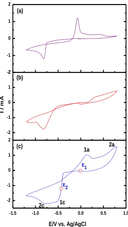
Figure 1. Cyclic voltammograms for DMSO solutions of: (a) 0.0075 M Bi (NO3)3, (b) 0.01 M TeCl4
and (c) 0.01 M TeCl4 + 0.0075 M Bi (NO3)3· + 1M Na NO3 (pH 3) in DMSO. Scan rate: 0.02
V·s-1
.
The voltammmetric response for Bi3+ dissolved in DMSO is presented in figure 1(a). The scan towards negative potential reveals the starting of the reduction at - 0.7 V, followed by a current peak at - 0.8 V associated to the theoretical value of a 3- electron reduction process [13], as follows:
(1)
On the reverse scan, a nucleation loop is observed followed by the stripping of bismuth characterized by an anodic peak with a maximum at ca. - 0.07 V. Figure 1(b) shows the cyclic voltammetric scan for Te4+ in DMSO. The reduction reaction begins at - 0.49 V, associated to Te4+ reduction to elemental tellurium through a four electron process:
Extending the scan towards more negative potentials reveals a peak at - 0.82 V, which is associated to Te reduction in DMSO according to reaction:
(3)
The tellurium stripping is observed in the reverse scan characterized by a weak peak at 0.30 V. When bismuth and tellurium precursors are presents in solutions (figure 1(c)) the voltammetric response undergoes some changes. During the negative potential scan Te4+ ions adsorbed at the electrode surface are reduced to Te2- at approximately - 0.35 V. Then, Bi3+ reacts with Te2- to form a tellurium rich Bi2Te3 phase according to [7]:
(4)
Following the cathodic scan another reduction peak (2c) is observed at - 0.84 V associated to diffusion controlled formation of Te2- from Te4+ to form the compound through the precipitation reaction,
(5)
In the anodic scan, two broad oxidation peaks are observed. The first one (1a) at 0.13 V corresponds to the deposited bismuth telluride stripping and the second (2a) attributed to Te oxidation.
3.2. Nucleation and growth mechanism analysis
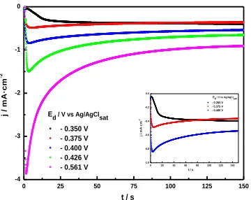
A set of E/t perturbation programs selected from the voltammetric results were employed in order to study the N.G.Ms of Bi2Te3. Figure 2 shows the respective j/t transient responses recorded
between - 0.350 V and - 0.561V where a homogeneous and adherent film is formed.
0 25 50 75 100 125 150
-4 -3 -2 -1 0
j
/
m
A
·c
m
-2
- 0.350 V - 0.375 V - 0.400 V - 0.426 V - 0.561 V
t / s
Ed / V vs Ag/AgClsat
0 20 40 60 80 100 120 140
-1.0 -0.8 -0.6 -0.4 -0.2 0.0
j
/
m
A
·c
m
-2
- 0.350 V - 0.375 V - 0.400 V
[image:5.596.207.387.549.692.2]t / s Ed / V vs Ag/AgClsat
Figure 2. Experimental j/t transients recorded on FTO using 0.01 M TeCl4 + 0.0075 M Bi (NO3)3 +
1M Na NO3 (pH 3) as deposition bath. The inset presents the j/t experimental transients
These transients exhibit an induction time for the nuclei formation which decreases as the applied potential is more negative. For Ed = - 0.350 V the nucleation phenomenon is slow, it can be
observed at around t < 2.5 s. After the induction time, the current density decreases until attaining an approximately constant value. At more negative potentials values, the current achieves a maximum which is associated to nuclei coalescence. Further, the current density decreases towards a constant value indicating the contribution of a diffusion process. A detailed study of each j/t transient was performed at different potentials following the theoretical NMGs model reported by Bewick et al. [14]. The fitting of the transients was made including 2D and 3D nucleation processes according to the following general relationship:
(6)
Where: s the contribution corresponding to an instantaneous nucleation process under charge- transfer control; is a 3D progressive nucleation process under charge- transfer control, and corresponds to a 3D instantaneous nucleation mechanism controlled by diffusion. Each j/t transient can be fitted by equation (6) as follows:
(7)
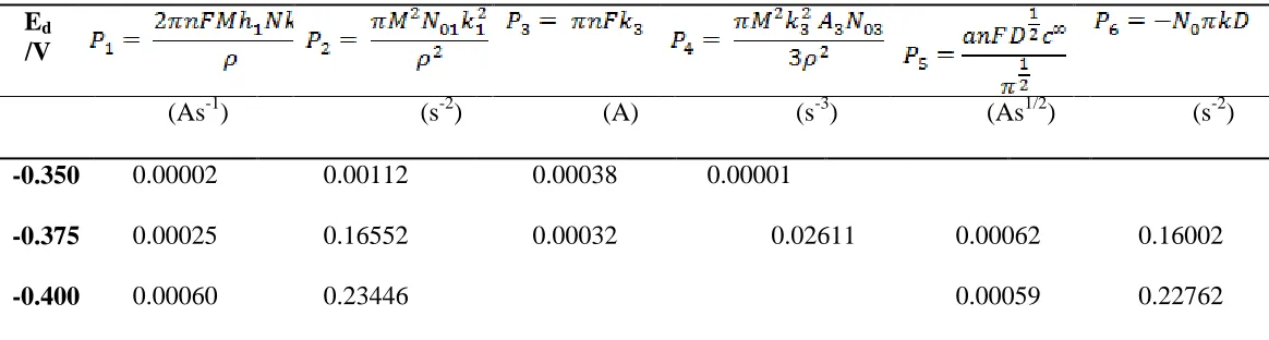
The Pi parameters obtained from this fitted equation and its physical meaning, are shown in
Table I.
Table I. Kinetic Parameters obtained by the Nonlinear Fitting for j/t transients and nucleation and growth proposed mechanisms.
Ed
/V
(As-1) (s-2) (A) (s-3) (As1/2) (s-2)
-0.350 0.00002 0.00112 0.00038 0.00001
-0.375 0.00025 0.16552 0.00032 0.02611 0.00062 0.16002
-0.400 0.00060 0.23446 0.00059 0.22762
Ed: Potential step value; n·F: molar mass c ar e transferred durin t e electrodeposition (A·s·mol-1
[image:6.596.7.589.504.660.2]
0,0 0,2
0,4 (a)
0,0 0,2 0,4
(b)
0 20 40 60 80 100 120 140
0,0 0,2 0,4 0,6 0,8 1,0
(c)
-
j
/
m
A
·c
m
-2
[image:7.596.184.406.93.435.2]t / s
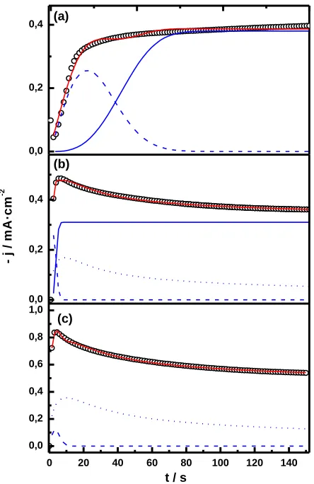
Figure 3. Experimental (o) and fitted (red line curve) j/t transients at (a) Ed =- 0.350 V, (b) Ed =- 0.375
V and, (c) Ed =- 0.400 V during the electrodeposition of Bi2Te3/FTO. The individual
contributions of the three mechanisms of nucleation and growth calculated from the parameters of Table I are also included: (IN-2D)ct (- - -), (PN-3D)ct (―), and (IN-3D)dif (···).
The data were fitted with equation (7) considering the individual contributions of the three MNGs through the Pi parameter of Table I. Figure 3 shows the experimental and fitted curves at the
selected potentials. In the case of electrodeposition at - 0.350 V (figure 3(a)), the deconvolution of the total density current involves only two contributions. At short times, the first one is associated to a 2D instantaneous nucleation controlled by charge transfer, (IN-2D)ct whereas at longer times the second
contribution corresponds to a 3D progressive nucleation also controlled by charge transfer, (PN-3D)ct.
Besides, no contributions related to a 3D instantaneous nucleation mechanism controlled by diffusion is observed at this potential. At more negative potentials (see figure 3 (b) y 3 (c)), the (IN-2D)ct
contribution appears at shorter times than at - 0.350 V, however at longer times there is a new contribution which is controlled by a diffusion process. Note that for Ed= - 0.400 V the simulation fits
very well along the whole length of the time interval considered. Besides, the fact that at short time almost immediately appears a (IN-3D)dif contribution seems to indicate that the 3D nuclei are
Regarding the kinetic parameters shown in Table I, it is possible to observe that P1, P2, P4 and,
P6 values increase as the potential is more negative a behavior that can be attributed to an increasing in
the nucleation rate. Furthermore, P3 and P5 parameters remain without changes given they are
independent of Ed.
3.3. Bi2Te3 electrodeposition
Taking account the Bi2Te3 MNGs study, a set of two steps E/t perturbation programs were
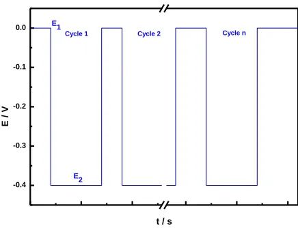
selected (see figure 4).
-0.4 -0.3 -0.2 -0.1 0.0
Cycle n Cycle 2
E2
E
/
V
t / s
E1
Cycle 1
Figure 4. E/t program selected for Bi2Te3 PED. Step 1: E1 = V; τ1 =2s, no net electrochemical
reduction processes take place. Step2: - .4 V ≤ E2 ≤ - .35 V τ2 =5s, Bi2Te3 deposition
takes place through reaction described by equation (5).
It is expected that under these conditions a 2D layer by layer growth be the process that controls the deposition resulting in homogenous films. Twelve cycles (T = 84s) were applied to obtain
films with the required thickness. To promote the 2D instantaneous nucleation the deposition times were restricted to 5s.
3.4. Films Characterization
3.4.1. Morphological characterization
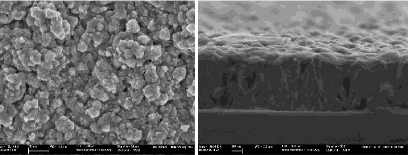
The morphological characterization of the films was made by SEM and AFM analysis. Similar morphologies were obtained for the films electrodeposited with the different potential/time programs studied. For Ed = - 0.400 V SEM images 5 (a) and (b) exhibit uniform granular morphology with an
[image:8.596.184.402.245.412.2][image:9.596.101.499.70.222.2]
Figure 5. (a)Surface morphology and, (b) cross-sectional SEM images for Bi2Te3/FTO thin film.
AFM images show a smooth aspect with a regular microstructure in agreement with SEM micrographs. Homogeneous deposition and roughness of about RMS = 94 nm were determinate.
Figure 6. AFM images of Bi2Te3 thin films onto FTO: (a) 2D and (b) 3D morphologies.
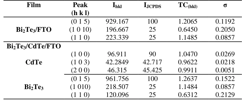
3.4.2. Structural characterization
The crystal structure of two films deposited by PED on different substrates (FTO and CdTe/FTO) was studied by XRD in the parallel eometry. In bot cases, four diffraction pea s can be observed in R patterns at 2 . 3 , 3 . 2 , 4 . and 5 . ° ic are related to t e ( ), ( 5), (1 0 10), (1 1 0) and (2 0 5) reflections of trigonal Bi2Te3 phase, (JCPDS, 15-0863) [15],
respectively. Thus, these results show that the samples are polycrystalline with a preferential orientation along the (0 1 5) direction. In the case of Bi2Te3/CdTe/FTO t e pea s located at 23. 3°,
a/a 32%). To assess the crystalline quality, the FWHM (Full Width at Half Maximum) for the preferential orientation as also calculated, t e values obtained ere . ° for Bi2Te3/FTO and . ° for
Bi2Te3/CdTe/FTO, indicating that the latter film has better crystalline quality and slightly grain size.
Employing the Scherrer equation for the (0 1 5) preferential orientation crystalline sizes of 40 and 42 nm were respectively calculated.
20 25 30 35 40 45 50 55
0 500 1000 1500 2000 2500 (2 0 5 ) (1 1 0 ) (1 0 1 0 ) (2 0 0 ) (1 0 3 ) (0 1 5 ) (1 0 0 )
Bi2Te3/CdTe/FTO
Bi 2Te3/FTO
I
(a
.u
)
[image:10.596.151.432.181.380.2]2 (º)
Figure 7. XRD pattern of (a) Bi2Te3/FTO and (b) Bi2Te3/CdTe/FTO deposited by PED technique.
Table II. Harris texture coefficients and standard deviations of Bi2Te3 /FTO and Bi2Te3/CdTe/FTO
films deposited by PED.
Film Peak
(h k l)
Ihkl IJCPDS TC(hkl) σ
(0 1 5) 929.167 100 1.2065 0.1192
Bi2Te3/FTO (1 0 10) 196.667 25 0.6450 0.2050
(1 1 0) 223.339 25 1.1485 0.0857
Bi2Te3/CdTe/FTO
(1 0 0) 96.911 90 1.0470 0.0269
CdTe (1 0 3) 42.2849 42.717 0.9622 0.0218
(2 0 0) 46.315 45.425 0.9911 0.0051
Bi2Te3
(0 1 5) (1 010) (1 1 0)
961.756 218.507 120.096 100 25 25 1.2637 1.1484 0.6312 0.1522 0.0857 0.2129
TC(hkl): Texture Coefficient,Ihkl: Intensity of the (hkl) peak observed in the
experiment,IJCPD:: Intensity of the (hkl)peak found in the literature [15,16], σ: t e
associated standard desviation.
[image:10.596.89.502.481.653.2]
than 1 meaning that the peak is associated to a preferential plane growing, confirming thus that the films is strongly oriented along the (0 1 5) direction.
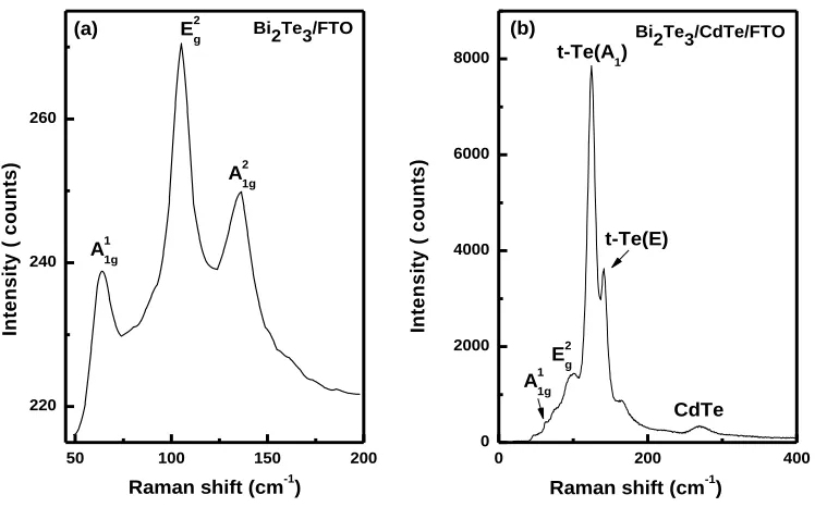
Raman spectra of the as-grown Bi2Te3 thin film recorded in the range 20 - 54 cm-1 and it is
depicted in figure 8 (a). The spectrum was analyzed to verify the Bi2Te3 and to look for the presence of
traces of other components which could be possible by means PED.
50 100 150 200
220 240 260 In te n s it y ( c o u n ts )
Raman shift (cm-1) E2g
A2 1g In te n s it y ( c o u n ts )
Raman shift (cm-1)
Bi2Te3/FTO
A11g (a)
0 200 400
0 2000 4000 6000 8000 (b) t-Te(E)
A11g E2
g
Bi2Te3/CdTe/FTO
t-Te(A1)
[image:11.596.111.485.194.427.2]CdTe
Figure 8. Typical Raman spectrums of (a) Bi2Te3/FTO and (b) Bi2Te3/CdTe/FTO thin films.
The Raman bands of Bi2Te3 show the vibrational modes centered at 63.24 cm-1, 101.98 cm-1
and 133.03 cm-1 correspond to the, A1g1, Eg2 and A1g2 phones modes respectively [17,18]. The A1g1
mode indicates the stretching mode along the c-axis within the Bi-Te quintuple layers. The Eg2 is
associated to an interplanar vibration mode [19]. This vibration mode corresponds to the vibration of Bi-Te quintuple layers along the c-axis which is presented in bismuth telluride films with near stoichiometric composition [20]. The A1g2 mode involves the bonding forces between the bismuth and
tellurium atoms. A slightly excess in Te is reflected in a widening and shift of the A1g2 mode, in
agreement with the EDX analysis. Likewise, the Bi2Te3/CdTe (see figure 8 (b)) films present the Eg2
mode associated to Bi2Te3 and the peak associated to A1g2 modes is hidden by the CdTe signal because
of the higher signal intensity presented by this material. The bands centered at 124.81 cm-1 and 141.31 cm-1 corresponds to the A1 and E phonon modes respectively. These Raman modes are attributed to the
presence of tensile stress on Te precipitates in CdTe [21]. The weak mode observed around 164.24 cm
-1
compromising any conclusion about Te inclusions on CdTe surface, and speculating that heating by laser light could break chemical bond producing Cd evaporation, thus leaving a Te excess at the surface.
3.4 3. Electrochemical characterization
The optoelectronic properties of the Bi2Te3 film samples were studied employing
electrochemical impedance spectroscopy measurements. The analysis of the interfacial capacitance vs potential data were analyzed from the Mott–Schottky equation written as [23]:
(8)
where C is the differential capacitance of the space-c ar e re ion, ε0, the permittivity of
vacuum, εr the relative dielectric constant (85) [24], ND the donor carrier density for n- type
semiconductor or NA the acceptor carrier density for a p- type semiconductor, V the electrode
potential, and VFB the flat band potential. Figure 9(a) presents the experimental curve of the plot 1/C2
vs V which shows a positive slope, confirming that the Bi2Te3 layer presents the semiconductor
characteristic of an n- type material. The intercept at the potential axis yields -0.65 V for the flat band potential. The apparent concentration of majority carriers (ND), calculated from the slope, is 2. 5 ∙
1018 cm-3, a value that is within those reported in the literature and also comparable to the bulk material which is around 1017-1018 cm-3 [25].
-0.8 -0.6 -0.4 -0.2 0.0
1x10¹²
2x10¹²
2x10¹²
2x10¹²
E
FP = - 0.661V
E / V
C
-2 /
c
m
4·
F
-2
(a)
-0.6 -0.4 -0.2 0.0 0.2
0 5 10 15
(b)
j /
·A
·c
m
-2
E / V
Figure 9. (a) Mott-Schottky plot and (b) I/E voltametric profiles carried out under conditions of darkness (---), light (---) and under chopped light (---) of Bi2Te3/FTO thin film deposited
by PED in 0.05 M Na2B4O7. White illumination of 1000 W.
A semiconductor electrode should to show rectifying behavior under the polarization regime corresponding to minority carrier current flow. It is expected that for a n-type material rectification be observed at potentials positive of the flatband value. Under illumination electron and holes are separated in the space charge region and further driven in opposite directions by the effect of the electric field. The n-type conductivity of Bi2Te3 predicts the apparition of a positive photocurrent as
[image:12.596.100.483.468.601.2]
current.. The photocurrent was recorded using an electrolytic solution containing 0.05 M Na2B4O7, pH
= 9.3. Figure 9(b) shows j/E potentiodynamic responses for the Bi2Te3/FTO electrode under different
experimental conditions: in darkness, under illumination, and under chopped light conditions. As the dark current density (Jd) is very small (about <10-8 µA) t en Bi2Te3 forms a blocking contact with the
electrolyte. Under white light illumination, the curve exhibits an anodic photocurrent Jph supporting the
n- type character of the film. The photocurrent onset agrees well with the flat band potential derived from the Mott-Schottky plot (EFB = -0.66 V vs. SCE) according to the relation that Jph α (VFB −V) [26].
4. CONCLUSIONS
PED technique has been successfully employed for the synthesis of Bi2Te3 thin films onto FTO
and CdTe/FTO substrates. A detailed chronoamperometric study allowed to looking for the best conditions for obtaining good quality films without the need of a post thermal treatment. SEM images revealed a good adhesion to the substrate and also high quality microstructure. EDX analysis gave a stoichiometric composition very close to the expected one. XRD analysis showed that the films grew in the trigonal phase without the presence of others phases, a consequence of using a non-aqueous solvent in the synthesis. Besides, the films showed n-type semiconducting behavior with a significant apparent carrier density concentration (around ND = 2. 5 · 18 cm-3). Further work will be devoted to
extend current results concerning to the back contact on CdTe based solar cells and evaluation of its performance.
ACKNOWLEDGEMENTS
This work has been supported by FONDECYT (Fondo de Desarrollo Cientifico y Tecnoló ico, C ile) through Project No. 3031451. M.A acknowledges the support received from Pontificia Universidad Católica de Valparaíso (C ile).
References
1. G.S. Nolas, J. Sharp, J. Goldsmid. Thermoelectrics: Basic Principles and New Materials Developments, Springer, New York (2001).
2. R. Tang, Z. Wang, W. Li, L. Feng, J. Zhang, L. Wu, B. Li, G. Zeng,W. Wang, Solar Energy Materials & SolarCells, 121(2014) 92.
3. A. Boulouz, A. Giani, F. Pascal-Delannoy, Journal of Crystal Growth, 170 (1997) 817. 4. R. Tang, Z. Wang, W. Li, L. Feng, J. Zhang, L.Wu, B. Li, G. Zeng, W. Wang, Solar Energy
Materials and Solar Cells, 121 (2014) 92 .
5. A. Bailini, F. Donati, M.Zamboni, V.Russo, M. Passoni, C.S Casari, A. Li Bassi, C.E Bottani, Applied Surface Science, 254 (2007) 1249.
6. D.-H. Kim, E. Byon, G.-H. Lee, S. Cho., Thin Solid Films, 510 (2006) 148.
7. M. S. Martín-González, A. L. Prieto, R. Grons y, T. Sand, A. M. Stacy. Journal of The Electrochemical Society, 149 (2002) C546.
8. P. Magri, C. Boulanger, J.M. Lecuire, J.Mater. Chem., 6(5) (1996) 773.
10.C. V. Manzano, A. A. Rojas, M. Decepida, B. Abad, Y. Feliz, O. Caballero-Calero, D.A Borca-Tasciuc and M. Martin-Gonzalez. J Solid State Electrochem., 17 (2013) 2071.
11.W.J. Li, W.L. Yu, C-Y Yen. Electrochimica Acta, 58 (2011) 510.
12.V. Richoux, S Diliberto, C. Boulanger, J.M. Lecuire. Electrochimica Acta, 52 (2007) 3053. 13.M. Pourbaix, Atlas of Electrochemical Equilibria in Aqueous Solutions, Pergamon Press, Oxford,
New York (1966).
14.A. Bewick, M. Fleischmann, H.R. Thirsk, Trans. Faraday Soc., 58 (1962) 2200.
15. Database: Joint Committee on Powder Diffraction- International Centre for Diffraction Data (JCPDS-ICDD). JCPDS, Card No 15-0863. (http://www.icdd.com).
16.Database: Joint Committee on Powder Diffraction- International Centre for Diffraction Data (JCPDS-ICDD). JCPDS, Card No 19-0193. (http://www.icdd.com).
17.O. Caballero-Calero, P. Diaz-Chao, B. Abad, C.V. Manzano, M.D. Ynsa, J.J. Romero, M.M. Rojo, M. Martin-Gonzalez, Electrochim. Acta ,123(2014) 117.
18.F. Song-Ke, L. Shuang-Ming, and F. Heng-Zhi, Chin. Phys. B., 23 (2014) 086301.
19.L.M. Goncalves, C. Couto, P. Alpuim, A.G. Rolo, F. Völ lein, J.H. Correia., Thin Solid Films 518 (2010) 2816
20.V. Russo, A. Bailini, M. Zamboni, M. Passoni, C. Conti, C. S. Casari, A. Li Bassiand C. E. Bottani, J. Raman Spectrosc.; 39(2008) 205.
21.A. S. Pine and G. Dresselhays, Phys. Rev. B, 4 (1971), 356.
22.M.J. Soares, J.C. Lopes, M.C. Carmo, and A. Neves, phys. stat. sol. (c) 1 (2004) 278.
23.Jaime González Velasco. Fotoelectroquímica de semiconductores. Su aplicación a la conversión y almacenamiento de energía solar, Editorial Reverté y Centro Editorial de la Universidad
Autónoma de Madrid (2 ).
24.W. Richter, H. Kö ler, and C. R. Bec er. P ys. Stat. Sol. (b) -1 (1977) 619. 25.S. Sugai, Jpn. J. Appl. Phys. 30 (1991) L1083.
26.N. Sato Electrochemistry at Metal and Semiconductor Electrodes. Elsevier, Amsterdam, (1998).