Faculty of Mechanical Engineering
EFFECT OF REFLOW TIME ON HARDNESS, ELECTRICAL
RESISTIVITY AND WETTABILITY OF CNT IN SAC305
Muhammad Hafizuddin Bin Ghazali
Bachelor of Mechanical Engineering
i DECLARATION
I hereby declare that this project report entitled “Effect of Reflow Time on Hardness, Electrical Resistivity and Wettability of CNT in SAC305” is the result of my own work except as cited in the references.
Signature : ………
Name : ………
ii APPROVAL
This report is submitted to the Faculty of Mechanical Engineering of Universiti Teknikal Malaysia Melaka (UTeM) as a partial fulfilment of the requirements for the degree of Bachelor of Mechanical Engineering with Honor. The member of the supervisory is as follow:
Signature : ………
Supervisor Name : ………
iii ABSTRACT
iv ABSTRAK
v DEDICATION
To my beloved father Haji Ghazali Bin Said,
My beloved mother Hajah Noraini Binti Mohd Zain,
My beloved brothers,
Muhammad Nai’musyahmi, Muhammad Hisyamuddin, Muhammad Nazmiuddin
My supportive sister
Nurliayana Nabilah
vi ACKNOWLEDGEMENT
First of all, I want to lay my deepest thanks to Allah S.W.T the most gracious, the most merciful, the most helpful and with all the highest praise for giving me the chance to complete this final year project hard journey successfully.
My gratitude also to my greatest guidance and inspirational Dr. Nor Azmmi Bin Masripan for all his kind supervision, advice and helpful to complete this project from the start to the end. Thanks for his assistance to help me through this journey.
Not to forget, I would like to express my appreciate and dedication towards Pn. Intan Fatihah Binti Ahmad for guidance and teach me all the knowledge and advise to conduct this project. Furthermore, also the same gratitude to all the staffs and students to help me complete this project.
vii TABLE OF CONTENT
DECLARATION i
APPROVAL ii
ABSTRACT iii
ABSTRAK iv
DEDICATION v
ACKNOWLEDGEMENT vi
TABLE OF CONTENTS vii
LIST OF TABLES xi
LIST OF FIGURES xii
LIST OF ABBREVIATIONS xv
LIST OF SYMBOLS xvi
CHAPTER 1: INTRODUCTION 1
1.1 Background of Study 1
1.2 Problem Statement 2
1.3 Objectives 3
1.4 Scopes of Projects 3
viii
CHAPTER 2: LITERATURE REVIEW 6
2.1 Reflow Soldering System Introduction 6
2.2 Reflow Soldering Process 7
2.3 Reflow Profile of Reflow Soldering 8
2.4 Reflow Oven Stage of Reflow Soldering 10
2.4.1 Preheat Stage of Reflow Soldering 10
2.4.2 Soaking Stage of Reflow Soldering 10
2.4.3 Reflow Stage of Reflow Soldering 11
2.4.4 Cooling Stage of Reflow Soldering 11
2.5 Effect of Temperature on Reflow Stage for SAC305 12 2.6 Effect of Time Above Liquidous (TAL) on Reflow Stage for SAC305 13
2.7 Study of Properties of SAC305 With CNT 14
2.7.1 SAC305 Microstructure Characterization Study 15
2.7.2 SAC305 Electrical Conductivity Test Study 17
2.7.3 SAC Hardness Test Study 18
2.7.4 SAC305 Wettability Test Study 19
2.8 Carbon Nanotube (CNT) Properties 21
CHAPTER 3: METHODOLOGY 22
3.1 Project Planning 22
3.2 Relation Between Objectives And Methodology 25
3.3 Methodology 26
3.3.1 Printed Circuit Board Developer Process 26
ix
3.3.4 Laser Cutting Process 33
3.3.5 Cold Mounting Process 34
3.3.6 Grinding And Polishing Process 38
3.3.7 Defect Observation Process 42
3.3.8 Measurement of Electrical Resistivity Testing Process 43
3.3.9 Measurement of Hardness Testing Process 45
3.3.10 Measurement of Wettability Process 47
CHAPTER 4: RESULT AND DISCUSSION 48
4.0 Overview 48
4.1 Observation Defect of SAC 305 + CNT 0.04 wt. % 49 4.1.1 Comparison of Defect of SAC 305 + CNT 0.04 wt. % using
Reflow Oven with Reflow Time 45, 60 and 75 seconds At 243 ºC.
49
4.2 Effect of Reflow Time to Electrical Resistivity of SAC 305 + CNT
0.04 w. t% 51
4.2.1 Comparison of Resistivity Effect of SAC 305 + CNT 0.04 wt. % using Reflow Oven with Reflow Time of 45, 60 and 75 seconds At 243 ºC
51
4.3 Effect of Reflow Time to Hardness of SAC 305 + CNT 0.04 wt. % 52 4.3.1 Comparison of Hardness Effect of SAC 305 + CNT 0.04 wt. %
using Reflow Oven with Reflow Time of 45, 60 and 75 seconds At 243 ºC.
52
4.4 Effect of Reflow Time to Wettability of SAC 305 + CNT 0.04 wt. % 54 4.4.1 Comparison of Wettability Effect of SAC 305 + CNT 0.04 wt. %
using Reflow Oven with Reflow Time of 45, 60 and 75 seconds At 243 ºC.
CHAPTER 5: CONCLUSION 56
x
5.2 Recommendation 57
REFERENCES 59
APPENDICES 63
Resistivity Result 64
xi LIST OF TABLES
TABLE TITLE PAGE
xii LIST OF FIGURES
FIGURE TITLE PAGE
1.1 Flow chart of the methodology 5
2.1 Reflow soldering product with electronic component soldered on
PCB 7
2.2 Ramp -To - Peak reflow profile 9
2.3 Soak reflow profile 9
2.4 Effect of reflow peak temperature to IMC thickness 12 2.5 Effect of reflow time (TAL) to IMC thickness 13 2.6 SEM image result for the SAC305 solder paste 16 2.7 SEM fractographs result for fracture surface of the composite;
a) and b) SAC305 + 0.01 wt. % Ag-coated SWCNTs c) and d) SAC305 + 0.1 wt. % Ag-coated SWCNTs
17
2.8 Uniform distribution of SAC microstructure; a) eutectic region area
b) Sn-Matrix
19
2.9 Microscope image of wettability of solder measured by contact
angle, θ between solder and the Cu-substrate. 20 2.10 Relationship of wt. % of Cu-coated SWCNTs and contact angle (º). 20 2.11 Properties of Single - Walled Carbon Nanotubes (SWCNT). 21
3.1 Flow chart of the project 24
3.2 Open positive PCB packaging 26
3.3 Printed Accublack paper with 4-dotted pattern 26
xiii 3.5 a) PCB developer machine
b) Inserting positive PCB into sodium carbonate 28
3.6 Etching machine 29
3.7 a) before etching process
b) after etching process 29
3.8 Photoresist stripper machine 30
3.9 Final product of PCB developer 30
3.10 Soaking process of the PCB into chemical 30
3.11 SAC305 + CNT 0.04 wt. % stirring process 31
3.12 Cutting positive board process using board cutter 32
3.13 Reflow oven profile 32
3.14 Reflow oven machine 33
3.15 Finished reflow process of the solder alloy 33 3.16 a) Laser cutter machine
b) Positive board mounted on the machine c) Drawing cutting design through computer
34
3.17 Positive board cut using laser cutter machine 34
3.18 Hardener Chemical 35
3.19 Resin Chemical 35
3.20 80 ml beaker and 10 ml measuring cylinder 35
3.21 Release agent 35
3.22 Paper cup 35
3.23 Glass rod 35
3.24 Cold mounting silicone rubber mold 36
3.25 Mixing resin and hardener process 36
3.26 Aluminum foil clip 37
xiv
3.28 Cold mounting process 38
3.29 Finished product 38
3.30 Grinder and polishing machine 39
3.31 Grinder and polisher machine controller 40
3.32 Grinding process 40
3.33 Image analyzer device 41
3.34 Etching process 41
3.35 Specimens IMC layer observed using image analyzer 42
3.36 Jandel Model RM3000 four-point probe 43
3.37 Calibration stage tool 44
3.38 Electrical resistivity measurement using Four Point Probe 44
3.39 Nano Indentation measurement device 45
3.40 Solder alloy sample hardness testing point level 46 3.41 Measuring wettability using Image J application 47
4.1 Image analyzer of SAC 305 + CNT 0.04 wt. % for reflow time a) 45 seconds,
b) 60 seconds c) 75 seconds
49
4.2 Solder alloy SAC 305 + CNT 0.04 wt. % average electrical
resistance with reflow time. 51
4.3 Solder alloy SAC 305 + CNT 0.04 wt. % average hardness with
reflow time. 52
xv LIST OF ABBREVIATIONS
PCB Printed Circuit Board
SAC305 Sn (Tin 96.5%), Ag (Silver 3%) and Cu (Copper 0.5%) CNT Carbon Nanotube
SEM Scanning Electron Microscope SMT Surface Mount Technology PWB Printed Wiring Board
TAL Time-Above-Liquidous
CTE Coefficient of Thermal Expansion IMC Intermetallic Compound
SWCNT Single-Walled Carbon Nanotubes
wt. % (Weight of solute / Weight of solvent) x 100 SiC Silicon Carbide
UV Ultraviolet
xvi LIST OF SYMBOLS
ºC Temperature in Celsius s Time in seconds
mA Current milliampere mR Resistance milliohm 𝑐𝑚2 Area centimeter square mbar Pressure millibar
ml Volume milliliter mm Scale millimeter
1 CHAPTER 1
INTRODUCTION
1.1. Background of Study
Soldering process of electronic component on Printed Circuit Board (PCB) had becoming more convenience and cheaper by using modern method of reflow soldering. Reflow soldering method is a process that use special solder paste (mixture of powdered solder and flux), that will be applied on the PCB contact pad. The solder paste will be subjected to controlled heat by using reflow oven, by certain range of temperature it will melt the solder paste and reflow them to join the electronic component with the PCB (Georgina Kearney, 2015).
2 important of SAC305 was its flexibility to be used by most of soldering equipment, existed processes method and solder flux (AIM Metals and Alloys LP, 2016).
Recently, the effort to improvise the solder paste was done by many researchers to see the effect of SAC305 properties in term of its mechanical and conductivity performance. Researchers had found that by adding low amount of Carbon Nanotube (CNT) into the SAC305 solder paste mixture, the characteristics of the solder paste will have positive change in term of its wetting, dispersion and reflow properties (K. Bukat, et al., 2012).
1.2. Problem Statement
3 1.3. Objectives
The objective of this project are as follows:
i. To study the defect of SAC305 when add with 0.04 wt. % CNT at different reflow duration.
ii. To investigate the properties of wettability, hardness and electrical resistivity of SAC305 when added 0.04 wt. % CNT.
1.4. Scopes of Projects
The scope of these project are as follows:
i. The solder paste that will be used for this project is SAC305 with 0.04 wt. % CNT.
ii. The reflow process is by using reflow oven.
iii. Analysis of the defect by using Image Analyzer (AI). iv. Study the electrical resistivity using Four-point probe.
v. Study the hardness using Nano-indentation.
4 1.5. General Methodology
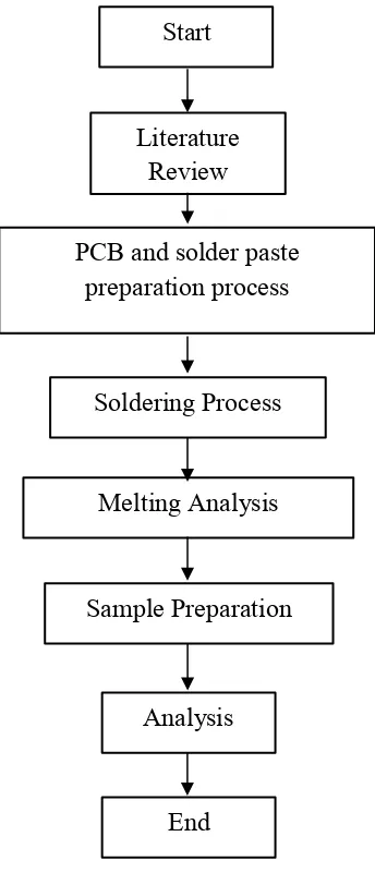
The explanations and details for methodology that will be execute in order to achieve the objectives in this project will be discuss. The flow of this project experiment will also be shown in this section.
1. Literature review
Collecting data through previous journals, website, articles and any related material about the project.
2. Material preparation.
Printed circuit board (PCB) and solder paste SAC305 with CNT will be prepare along with the measurement devices and tools to execute the experiment.
3. Experiment
The experiment will focusing on heat treatment of the SAC305 by applying variances time duration in the reflow oven with constant temperature setting.
4. Sample preparation
After cooling period, the SAC305 with CNT will be take out to be analysis.
5. Analysis
5 The methodology of this study is simplify in the flow chart as shown in Figure 1.1.
Figure 1.1: Flow chart of the methodology. Literature
Review
End Analysis Sample Preparation
Melting Analysis Start
Soldering Process PCB and solder paste
6 CHAPTER 2
LITERATURE REVIEW
2.1 Reflow Soldering System Introduction
The capability of reflow soldering to integrate with Surface Mount Technology (SMT) had expanded the reflow soldering method by study, refined and improvement. There are two main reason of the usage of the reflow soldering over other conventional methods.
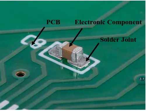
The first reason is the advantage of the reflow soldering method which are usually had uniform solder joint effect with the electric component. The properties of this solder also usually more cleanliness during completed assembly make it more tidy and better quality. It have higher flexibility that make it to able to solder a large number of electronic component with minimum changeover of time thus increase production rate.
7 to minimize the solder grain growth allow it to become more durable solder joint. More, process overall have less pressure and damage applied on the PCB, thus reduce defect product. Plus, the process also have less movement of part make the component more neatly and tidy, refer to Figure 2.1. (Jim Bergenthal, 1995).
Figure 2.1: Reflow soldering product with electronic component soldered on PCB.
2.2 Reflow Soldering Process
The reflow soldering not only low cost to maintain it is also simpler process compare to the conventional soldering process. Basically, reflow soldering process required three important component from the solder paste preparation, electronics component placement and heat application or reflow soldering process. These process is important for reflow soldering to get a good result.