MULTI-SCALE SIMULATIONS OF SINGLE-WALLED CARBON NANOTUBE ATOMIC FORCE MICROSCOPY AND DENSITY FUNCTIONAL THEORY CHARACTERIZATION OF FUNCTIONALIZED AND NON-FUNCTIONALIZED
SILICON SURFACES
Thesis by
Santiago de Jesus Solares Rivera
In Partial Fulfillment of the Requirements for the Degree of
Doctor of Philosophy
California Institute of Technology Pasadena, California
2006
ii
iii
ACKNOWLEGEMENTS
I thank God for life, family, and friends, and for all the gifts He constantly gives us. I cannot even begin to count all the good things I have received.
I thank my wonderful wife, Melissa, for being a loving and supporting companion. I thank my parents, Santiago and Catalina, for providing me with a loving home and for all their hard work in raising our family. I thank my siblings, Arturo and Doris, for adding color to my life.
I thank the rest of our family and friends in various countries, who in so many ways have contributed and continue to contribute to all the things in which I participate.
I thank my advisor, professor William Goddard, for the many opportunities he has provided me with, for everything he has taught me, and above all for his friendship and trust.
I thank my co-advisors and instructors, Doctors Mario Blanco (a very generous and supportive friend who has spent so much of his busy time teaching me many of the methods upon which my research rests) and Siddharth Dasgupta, Professors Pat Collier, Jim Heath, and Nate Lewis, as well as the Chemical Engineering Faculty, especially Professors Zhen-Gang Wang and Konstantinos Giapis, for their teaching, guidance, and friendship. Very special thanks also to Kathy Bubash.
iv teachers and mentors at previous institutions for sharing their lives and experiences with me.
v
ABSTRACT
vi
TABLE OF CONTENTS
ACKNOWLEDGEMENTS ……….… iii ABSTRACT …...……….……… v TABLE OF CONTENTS ………. vi CHAPTER 1: INFLUENCE OF ELASTIC DEFORMATION ON SINGLE-WALLED CARBON NANOTUBE AFM PROBE RESOLUTION ……….…… 1 CHAPTER 2: MECHANISMS OF SINGLE-WALLED CARBON NANOTUBE
PROBE-SAMPLE MULTISTABILITY IN TAPPING MODE AFM IMAGING ……. 38 CHAPTER 3: INFLUENCE OF CARBON NANOTUBE PROBE TILT ANGLE ON EFFECTIVE PROBE STIFFNESS AND IMAGE QUALITY IN TAPPING-MODE ATOMIC FORCE MICROSCOPY ………...……….. 83 CHAPTER 4: DENSITY FUNCTIONAL THEORY STUDY OF THE GEOMETRY, ENERGETICS AND RECONSTRUCTION PROCESS OF SILICON (111) SURFACES ……….… 119 CHAPTER 5: STRUCTURE OF THE METHYLATED SILICON (111) SURFACE PREPARED THROUGH HYDROGENATION-CHLORINATION-ALKYLATION ………..180 CHAPTER 6: QUANTUM MECHANICS CALCULATIONS OF THE
1
Chapter 1: Influence of Elastic Deformation on Single-Walled Carbon
Nanotube AFM Probe Resolution
*ABSTRACT. We have previously reported that 4-6 nm diameter single wall carbon nanotube (SWNT) probes used for tapping-mode atomic force microscopy (AFM) can exhibit lateral resolution that is significantly better than probe diameter when imaging prone nanotubes on a flat SiO2 surface. To further investigate this phenomenon, accurate
models for use in atomistic molecular dynamics simulations were constructed based on transmission electron microscopy (TEM) and atomic force microscopy (AFM) data. Probe-sample interaction potentials were generated utilizing force fields derived from ab initio quantum mechanics calculations and material bulk and surface properties, and the resulting force curves were integrated numerically with the AFM cantilever equation of motion. The simulations demonstrate that under the AFM imaging conditions employed elastic deformations of both the probe and sample nanotubes result in a decrease of the apparent width of the sample. This behavior provides an explanation for the unexpected resolution increase and illustrates some of the subtleties involved when imaging with SWNT probes in place of conventional silicon probes. However, the generality of this
* Reproduced with permission from Shapiro, I.R.; Solares S.D.; Esplandiu, M.J.; Wade, L.A.; Goddard
W.A. III; and Collier C.P.; J. Phys. Chem. B 2004, 108, 13613. Copyright 2004 American Chemical
2 phenomenon for other AFM imaging applications employing SWNT probes remains to be explored.
1. Introduction
To date, numerous papers have described the preparation of both multi-wall and single-wall carbon nanotube AFM probes.1-5 SWNT probes offer topographic imaging resolution superior to that of conventional silicon AFM tips due to their unique chemical and mechanical properties, high aspect ratios, and molecular-scale dimensions.6-10 In a recent publication we described an efficient SWNT probe fabrication methodology and correlated the structures (acquired by TEM) of 14 probes with the quality of AFM images they produced when imaging a prone SWNT sample.11 By comparing the observed AFM resolution with the diameter of the probe nanotube measured from the TEM image, we found that the lateral resolution is on average 1.2 times the nanotube probe diameter. This value approaches the expected ideal ratio of unity in the absence of thermal vibrations and bending effects of the probe.12
3 Figure 1. In an ideal case, the limiting resolution equals the diameter of the probe. This simplified model, in which the probe and sample are considered to be incompressible objects, has commonly been used to describe AFM resolution.2,4,5 However, simple geometrical arguments alone cannot explain the sub-diameter resolution we reported. The potential for SWNT AFM probes to be used as common research tools requires a more thorough understanding of how the physical, chemical, and mechanical properties of SWNT probes affect image resolution.
Figure 1: Schematic illustration of the relationship between probe diameter and lateral resolution. The left panel shows a model for a SWNT probe imaging a prone nanotube on a flat surface. The right panel shows the resulting cross sectional profile, from which the width and height of the imaged nanotube are measured. In this simple geometric model, the full width is equal to the sum of the diameters of the probe and sample nanotubes.
4 The dimensions of the probes and samples are on the order of 1-50 nm, placing them within the range of atomistic simulations. To elucidate the actual tip-sample interactions that give rise to the observed phenomena, we have used TEM - AFM correlation data11 to construct realistic molecular models of an open-ended SWNT probe interacting with a prone SWNT sample on a flat hydroxyl-terminated silicon surface. These models were used to generate accurate potential curves at different positions of the probe relative to the sample. Integration of the resulting forces into the equation of motion for an oscillating cantilever yielded simulated topographic cross-section profiles that corroborate the experimental results. These simulations indicate that under the AFM conditions employed, both probe bending and localized deformations of the probe and sample SWNTs strongly influence the topographic profile measured with AFM. The reversible elastic nature of these deformations is demonstrated both experimentally and in simulations.
2. Methods
5 repeated measurements of the sample nanotube height as a function of probe oscillation amplitude were performed for both conventional silicon and SWNT AFM tips. In all cases, the driving amplitudes employed were kept below the limit corresponding to a 10% reduction in the apparent height of the sample nanotube due to compression. In addition, we measured force calibration curves, which consist of scans of the damped oscillation amplitude as a function of the average tip-sample separation for a given cantilever driving force. The force calibration curves revealed the presence of coexisting attractive and repulsive tip-sample interaction regimes.13,14 Bistable switching of the cantilever oscillation between the two regimes manifests itself as sudden changes in the observed sample height and width.15 In general, we avoided these amplitude instabilities and the concomitant experimental artifacts by operating the AFM cantilever with a driving force sufficient to give a free-air oscillation amplitude greater than 20 nm. Consequently, all AFM data presented here can be considered in the repulsive regime or “intermittent contact” mode.
The simulation of the AFM tip motion was carried out by integrating the equation of motion for a damped harmonic oscillator at each AFM scan point on the sample using the experimental parameter values contained in Table 1:
) cos( ) ( ) , ( ) , ( ) , ( 2 2 t F z F dt t Z dz Q m t Z kz dt t Z z d
m ts ts o
c o c
c =− − ω + + ω ,
(1)
where z(Zc,t) is the instantaneous tip position with respect to its average position (Zc), k is the harmonic force constant for the displacement of the tip with respect to its equilibrium
rest position, m is the effective mass, ω0 = k/m is the free resonant frequency, Q is
6
is the calculated tip-sample interaction force, and Focos(ω t) is the oscillating driving force applied to the cantilever.
Table 1: Tapping-mode AFM parameters used for numerical simulations.
Cantilever spring constant k = 4.8 N/m
Cantilever quality factor Q = 150
Cantilever resonant frequency ω/2π= 47.48 kHz
Free air oscillation amplitude Ao = 39 nm
Amplitude set-point Asp = 15.4 nm
Excitation force Fo = 1.25 nN
7 Prior to integrating Equation (1) we obtained the required tip-sample interaction forces using atomistic models, as explained in detail below. All molecular dynamics (MD) simulations were carried out using Cerius2 molecular simulations software (Accelrys, San Diego, CA). The MD force field parameters were optimized by fitting the material bulk and surface properties such as elasticity moduli, vibrational frequencies, and surface geometry both to experimental data and to rigorous quantum mechanics calculations on clusters representative of the silicon and graphene systems under study. Equation (1) was integrated using the Verlet algorithm to fourth-order accuracy for the tip position and second-order accuracy for the tip velocity.18
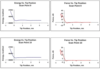
Realistic atomistic models were constructed for the SWNT probe used for tapping mode AFM imaging. Every effort was made to match the model structures and simulation conditions as closely as possible to corresponding experimental values, including the nanotube probe diameter, length, angle relative to the substrate normal, and the fine structure at the probe end. All silicon surfaces were (100) and were terminated with hydroxyl groups. The probe was a (40,40)19 armchair SWNT (5.4 nm diameter, 45 nm length, with 5 nm of fixed atoms at one end of the probe to simulate its attachment site at the AFM tip) constructed from approximately 25,000 carbon atoms. The sample was a (16,16) armchair SWNT (2.2 nm diameter, 10 nm length) constructed from approximately 2600 carbon atoms. The sample SWNT was kept fixed at both ends during the calculations to simulate a very long nanotube, which is unlikely to displace laterally during AFM tapping. Similar models were generated for a conventional silicon tip interacting with the sample nanotube. Several of these models are shown in Figure 2.
8 geometry by minimization of the potential energy (additional calculations performed at 300 K showed that the potentials did not significantly change with inclusion of thermal vibrations at room temperature. See supporting information). The gradient of this energy-position function with respect to the vertical tip position is the tip-sample interaction force.
In order to reduce the computational cost of the molecular simulations, each model of a nanotube on the surface included only a small section of the silicon surface, sufficient to obtain an accurate description of the SWNT probe interactions with the sample. This does not give an accurate description of the interaction of the tip with the silicon surface for the cases in which the SWNT tip deforms and slips against one side of the sample nanotube and makes contact with the underlying substrate. To correct this, another model was constructed without a sample nanotube on the substrate to obtain the interaction forces between the tip and the bare silicon surface. The deformation of the tip was considered in all cases when calculating the relative position of the surface and the end of the tip for each scan point.
9
Figure 2: Illustration of the models used to construct the tip-sample interaction profile. The models were constructed based on experimental TEM and AFM data. The final tip position during the AFM scan is shown for four of these points. The corresponding force curves are shown in Figure 3.
3. Results and Discussion
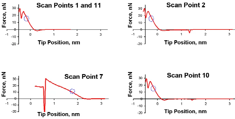
tip-10 sample force curves are shown in Figure 3 (all 11 energy-position curves, from which these force curves were obtained by differentiation, are provided in the supporting information). The abscissa on all graphs in Figure 3 corresponds to the distance between the lowest atom on the SWNT tip and the highest atom of the Si(100)-OH surface. Negative values on this axis correspond to elastic deformations in nanotube and surface geometry, including local deformation of the probe as well as slight deformation of the Si-OH surface.
11 Each of the eleven probe-sample force curves generated along the scan line was then inserted into Equation (1) and integrated for the average tip positions relative to the substrate (Zc) ranging from 50 to zero nm using actual imaging parameter values11. For each scan point and tip position, Equation (1) was integrated numerically for 0.02 seconds with a 0.1 ns integration step (to fourth order accuracy with respect to the time step-size) to determine the oscillation amplitude of the cantilever as a function of its vertical position (the initial tip position was set equal to its equilibrium position, i.e., z(Zc,0) = 0, and the initial velocity was set to zero in all cases). This numerical procedure is analogous to acquiring a “force calibration curve” for each scan point in Figure 2.
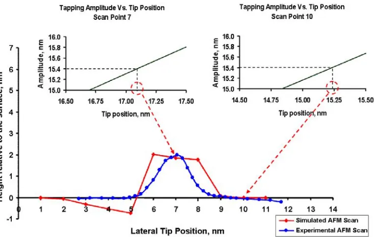
The result of these calculations was a curve showing the cantilever equilibrium oscillation amplitude as a function of the average vertical position of the tip for each point along the scan direction. Two of these curves are shown as insets in Figure 5. The simulated cross-section trace in Figure 5 was then constructed by plotting the locus of tip position values, which maintained the oscillation amplitude at the set-point value of 15.4 nm. Note that the average tip-sample separation for each scan point is given relative to the bare silicon oxide substrate.
12 amplitude bistability.13 However, at the free oscillation amplitude employed here, A0 = 39
nm, the average force will be determined almost exclusively by the repulsive part of the tip-sample interaction potential,16 and thus the underestimation of the attractive contribution will have negligible influence on the simulated topographic profile.
Under ambient conditions, a thin film of water is adsorbed on hydrophilic surfaces such as SiO2. The formation of a meniscus, or liquid bridge between the surface and the probe,
will result in an additional attractive capillary force that depends on probe-sample distance.21 We did not include the effects of adsorbed water in our model. We do not expect that inclusion of these effects will significantly change the nanoscopic interactions between the probe and sample nanotubes predicted by the simulations. Future work will address this issue.
Simple models of AFM resolution assume that the probe is a rigid, incompressible cylinder with a flat or hemispherical end. In practice this is not the case. High magnification TEM images show that the ends of the probe nanotubes are generally open due to ablation from an electrical etching procedure used to shorten the nanotube probes to useful lengths.2,4 Purely geometric arguments suggest that an open-ended tube with protruding asperities could, for extremely low-relief samples, provide resolution comparable to the asperity diameter rather than the full diameter of the probe, in direct analogy to results published using silicon probes.22 However, probe asperities are unlikely to be important when imaging a sample nanotube that has a diameter (height above the surface) comparable to that of the probe.
13 SWNT probes are susceptible to bending due to their high aspect ratio if not oriented vertically relative to a surface.12 This bending can be minimized by shortening the nanotube probe so that it protrudes less than 100 nm beyond the supporting silicon tip.
While SWNTs have exceptional longitudinal stiffness, radially they are far more compliant,24 a characteristic which permits localized deformation of the nanotube walls in addition to large-scale bending along the tube axis. The susceptibility of nanotubes to radial deformation is predicated upon two competing effects: the energy cost associated with strain of the nanotube as it is deformed from its equilibrium cylindrical geometry and the stabilization that a compressed nanotube gains due to increased interlayer van der Waals attractions. These two competing effects scale in opposite directions with increased nanotube diameter, such that larger SWNTs are easier to deform radially than smaller diameter tubes.25 We have previously observed that SWNTs attached to silicon AFM tips via the pick-up method tend to be 4-6 nm, which is larger than the tubes observed lying prone upon the pick-up substrate (1-3 nm).11 We postulated that the increase in net binding energy with larger diameter nanotubes stems from the interplay between van der Waals forces and the geometric stiffness of a nanotube. The resulting radial “softness” of these larger nanotubes not only increases the energy with which they bind to a silicon probe during pick-up, but also has significant implications when they are subsequently used for AFM imaging.
14 and the position (in the x-y plane) of the probe nanotube relative to the sample nanotube. The smaller the x-y distance between the center of the probe tube and the axis of the sample tube, the larger the force required to deform the nanotubes and cause them to slip past one another. That is, when the probe presses on the edge of the sample nanotube, a smaller amount of force is required to cause it to slip laterally than when it presses on the crown of the sample nanotube. The simulations show this deformation behavior to be completely reversible and elastic (images illustrating reversibility are provided in the supporting information). Experimentally, the elasticity is demonstrated by the fact that we have not observed the topographic cross sections to change significantly during imaging at a given amplitude set-point, and the TEM images taken of each probe subsequent to AFM imaging show no alterations of the nanotube structure, such as kinks or buckles.
15 due to the larger diameter of the probe (5.4 vs. 2.2 nm), which decreases its radial rigidity.
This lateral slipping and deformation of the probe nanotube explains the observation of sub-probe-diameter effective resolution. In amplitude-feedback tapping mode AFM, modulation of the cantilever oscillation amplitude depends on the average strength of the tip-sample forces.26 The AFM controller adjusts the extension of the z-piezoelectric element in order to hold the amplitude of the cantilever oscillation at the fixed value designated by the amplitude set-point (an independent variable set by the user). The resulting z-piezo voltage corrections are converted to units of length and output as the topographic height data. If the probe and sample deform negligibly under the associated tapping forces, the sample height can be measured accurately to within the precision of the piezoelectric element, typically < 1Å. However, if either material is significantly deformable, the resultant z-piezo data represents a more complex convolution of probe and sample structure.
16 SWNT and the Si/SiO2 surface. Thus, for that particular x-y position, the AFM
controller does not “see” the sample nanotube. Only when the probe SWNT is positioned closer to the crown of the prone sample SWNT are the interaction forces between the probe and sample nanotubes high enough to cause sufficient damping of the cantilever oscillation amplitude. At scan point 7, which corresponds to the probe tapping on the crown of the sample nanotube, no slipping can take place under the imaging conditions given in Table 1 because the maximum tip-sample repulsive force does not exceed the necessary threshold: ~30 nN. Here, the cantilever amplitude is damped by the sample nanotube, and the AFM records the interaction. The net result is that the topographic data indicates an apparent nanotube width which is smaller than the sum of the probe and sample SWNT diameters.
17
Figure 5: Schematic depiction of the construction of an AFM scan from molecular and AFM dynamics simulations. The two inset amplitude-distance curves illustrate how the measured height is obtained for each scan point at an amplitude set-point of 15.4 nm. The resulting AFM cross sectional height is given relative to the average tip separation from the bare SiO2 surface. The horizontal axis corresponds to the scan points shown in
Figure 2. For comparison, the cross section from experimental data has been overlaid on the same scale with its center point arbitrarily positioned to match up with the center of the simulated cross section.
18 attractive van der Waals forces between the larger silicon tip and the silicon surface. These two parameters in particular, probe compressibility and adhesion forces, are transformed in a highly nonlinear way by the response of the oscillating tip.27 Thus, SWNT probes perform in a fundamentally different manner than silicon probes, not merely when imaging prone carbon nanotubes, but for a variety of samples.
We have also simulated a smaller diameter SWNT probe since previous reports have described nanotube probes in the 1-3 nm diameter range.1,2,4,7 Smaller diameter nanotube probes should be far less susceptible to localized radial deformation due to their increased geometric stiffness against compression (as seen with the sample nanotube, Figure 4). However, the bending mode along the length of a thinner probe should actually be softer since the flexural rigidity scales as r4.28 The probe was a (16,16) armchair SWNT (2.2 nm diameter, 20 nm length) which had approximately the same aspect ratio as the larger 5.4 nm probe used in this study. As before, the probe nanotube was oriented at 15˚ relative to the surface normal, and the sample nanotube was 2.2 nm in diameter and 10 nm in length. Images from the simulation are incorporated in the supporting information and show that slipping also occurs for the thinner probe when tapping on the edge of the sample nanotube. For this probe, the slipping is almost entirely due to bending and not to local deformation. The corresponding tip-sample force curve indicates that the force opposing the slipping motion of the probe was negligible.
19 deformation of 1-3 nm single-wall carbon nanotubes by both van der Waals forces and external static loads.30-32 Here we show that in tapping-mode AFM, the associated forces deform the probe nanotube in addition to the sample, strongly influencing the subsequently measured effective lateral resolution.
Our molecular dynamics simulations confirm that some vertical compression of a prone sample nanotube occurs under standard tapping-mode AFM conditions for both conventional silicon AFM probes and SWNT probes. However, the simulations predict that this effect is, at most, 10% of the sample tube diameter for 1-3 nm SWNTs and occurs primarily when the probe nanotube is tapping on the crown of the sample nanotube (see for example, point 7 in Figure 2). This corresponds well with our experimental calibration of sample tube compression under the tapping mode operating parameters employed. The increase in lateral resolution, on the other hand, is due to the highly localized deformation and bending of the probe nanotube along the edges of the sample nanotube and is therefore not affected significantly by vertical compression.
4. Conclusions
20 interested in determining whether a similar increase of apparent resolution is observed when imaging less compliant samples, such as metallic or semiconducting nanoparticles.
Given the interest in nanoscale physical and biological phenomena, SWNT probes are likely to evolve into a more common research tool. A complete understanding of probe behavior in the context of atomic force microscopy is therefore critical. It is important to note that the lateral resolution reported here is an apparent value, arising from the simplified definition set forth in the introduction, and was studied for the specific case of 4-6 nm diameter SWNT probes imaging 2-3 nm diameter SWNTs adsorbed on a flat surface. In practice, the resolving power of an AFM probe is dependent upon the experimental context. It is of particular importance to determine whether the observed deformation phenomenon results in a net gain or loss of structural information when SWNT probes are used to image soft nanoscale samples such as biological macromolecules. The improvement in the apparent resolution due to radial deformation of the probe nanotube in this study was a consequence of the relatively high driving forces applied to the AFM cantilever. Tapping mode AFM imaging performed in this repulsive regime with conventional probes has been shown to damage biomolecules.14 In addition, resolution less than the probe diameter could complicate interpreting AFM images quantitatively.
21 Acknowledgement: The authors thank Professor Stephen Quake, Dr. Jordan Gerton and Ms. Yuki Matsuda for essential discussions. Ian Shapiro, Maria Esplandiu and Patrick Collier were supported by Caltech startup funds, and by Arrowhead Research. Santiago Solares and William Goddard were supported by NSF-NIRT grant CTS-0103002. Wade was supported by the Caltech President's Fund and NASA contract NAS7-1407.
SUPPORTING INFORMATION
1. Tables of force field parameters:
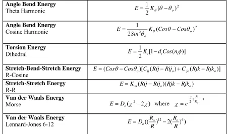
TABLE S-1: Force Field Energy Expression
Total Energy E = Ebond stretch + Eangle bend + Etorsion + Estretch-bend-stretch +
Estretch-stretch + Evan der Waals *
Bond Stretch Energy Type Harmonic
2
) (
2 1
o
b R R
K
E = −
Bond Stretch Energy Type Morse
2 )
( 1)
( −
= − R−Ro
o e
D
E α where
o b
D K 2
=
22
Angle Bend Energy
Theta Harmonic E= 12Kθ(θ −θo)2
Angle Bend Energy
Cosine Harmonic 2 2 ( )2
1
o o
Cos Cos
K Sin
E θ θ
θ θ −
=
Torsion Energy
Dihedral E= 21Kt[1−dtCos(ntφ)]
Stretch-Bend-Stretch Energy
R-Cosine E=(Cosθ −Cosθo)[Cij(Rij−Rijo)+Cjk(Rjk−Rjko)] Stretch-Stretch Energy
R-R E=Kss(Rij−Rijo)(Rjk−Rjko)
Van der Waals Energy
Morse E=Do(χ2−2χ) where
) 1 (
2 −
−
= Ro
R
e γ
χ
Van der Waals Energy
Lennard-Jones 6-12 E=Do((RRo)12−2(RRo)6)
[image:28.612.97.547.72.338.2]* The present study did not consider charged samples or probes; hence the energy expression does not include electrostatic energy terms.
TABLE S-2: Force Field Atom Types
H_ Non-acid hydrogen
H___A Acid hydrogen
C_3 SP3 carbon
C_2G SP2 graphite carbon
O_3 SP3 oxygen
Si0 Bulk silicon
SiS Surface silicon
SiOH Surface silicon connected to OH group
23
TABLE S-3: Harmonic Bond Stretch Parameters
Atom 1 Atom 2 Kb Ro
SiOH O_3 700.0000 1.5870
O_3 H___A 500.0000 1.0000
C_3 H_ 662.6080 1.1094
C_3 C_3 699.5920 1.5140
C_2G H_ 700.0000 1.0200
C_2G C_3 739.8881 1.4860
H_ H_ 700.0000 0.7500
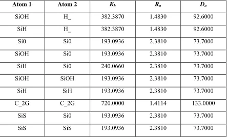
TABLE S-4: Morse Bond Stretch Parameters
Atom 1 Atom 2 Kb Ro Do
SiOH H_ 382.3870 1.4830 92.6000
SiH H_ 382.3870 1.4830 92.6000
Si0 Si0 193.0936 2.3810 73.7000
SiOH Si0 193.0936 2.3810 73.7000
SiH Si0 240.0660 2.3810 73.7000
SiOH SiOH 193.0936 2.3810 73.7000
SiH SiH 193.0936 2.3810 73.7000
C_2G C_2G 720.0000 1.4114 133.0000
SiS Si0 193.0936 2.3810 73.7000
24 TABLE S-5: Angle Bend Parameters
Atom 1 Atom 2 Atom 3 Type Kθ θo
C_2G C_2G C_2G Cosine harmonic 196.1300 120.0000
C_2G C_2G C_3 Cosine harmonic 196.1300 120.0000
C_3 C_2G C_3 Cosine harmonic 188.4421 120.0000
C_2G C_3 C_2G Cosine harmonic 220.2246 109.4710
C_3 C_3 C_3 Cosine harmonic 214.2065 109.4710
C_3 C_2G H_ Cosine harmonic 98.7841 120.0000
Si0 SiH H_ Cosine harmonic 42.2500 115.1400
Si0 Si0 Si0 Cosine harmonic 31.2682 105.0467
C_3 C_3 H_ Cosine harmonic 117.2321 109.4710
C_2G C_3 H_ Cosine harmonic 121.6821 109.4710
C_2G C_3 C_3 Cosine harmonic 220.2246 109.4710
C_2G C_2G H_ Cosine harmonic 103.1658 120.0000
Any O_3 Any Theta harmonic 100.0000 104.5100
H_ SiOH H_ Cosine harmonic 58.2560 110.9530
Si0 SiOH O_3 Cosine harmonic 102.7429 109.4710
SiOH SiOH Si0 Cosine harmonic 31.2682 105.0467
SiOH Si0 Si0 Cosine harmonic 31.2682 105.0467
SiOH Si0 SiOH Cosine harmonic 31.2682 105.0467
SiH SiH Si0 Cosine harmonic 31.2682 105.0467
Si0 SiH Si0 Cosine harmonic 31.2682 105.0467
SiH Si0 SiH Cosine harmonic 31.2682 105.0467
SiS Si0 Si0 Cosine harmonic 31.2682 105.0467
25
Si0 SiOH Si0 Cosine harmonic 31.2682 105.0467
SiOH SiOH O_3 Cosine harmonic 102.7429 109.4710
SiH SiH H_ Cosine harmonic 42.2500 115.1400
Si0 SiS Si0 Cosine harmonic 31.2682 105.0467
SiS SiS Si0 Cosine harmonic 31.2682 105.0467
O_3 SiOH H_ Cosine harmonic 57.6239 109.4710
TABLE S-6: Torsion Parameters
Atom 1 Atom 2 Atom 3 Atom 4 Kt nt dt
C_2G C_2G C_2G C_2G 85.1200 2.0000 1.0000
Any C_2G C_2G Any 100.0000 2.0000 1.0000
Any C_2G C_3 Any 2.0000 3.0000 -1.0000
Any C_3 C_3 Any 2.0000 3.0000 -1.0000
Any SiOH O_3 Any 2.0000 3.0000 -1.0000
TABLE S-7: Stretch-Bend-Stretch Parameters
Atom 1 Atom 2 Atom 3 Rij Rjk θo Cij Cjk
Si0 Si0 Si0 2.3810 2.3810 109.4712 -14.8184 -14.8184
TABLE S-8: Stretch-Stretch Parameters
Atom 1 Atom 2 Atom 3 Kss Rijo Rjko
26 TABLE S-9: van der Waals Parameters
Atom 1 Atom 2 Type Do Ro γ
H_ H_ Morse 0.018145 3.56979 10.70940
H___A H___A LJ 6-12 0.000099 3.19499 N/A
C_3 C_3 LJ 6-12 0.146699 3.98300 N/A
C_2G C_2G Morse 0.098999 3.993999 10.96300
O_3 O_3 LJ 6-12 0.095700 3.404599 N/A
Si0 Si0 LJ 6-12 0.310000 4.269999 N/A
SiS SiS LJ 6-12 0.310000 4.269999 N/A
SiOH SiOH LJ 6-12 0.310000 4.269999 N/A
SiH SiH LJ 6-12 0.310000 4.269999 N/A
C_2G H_ Morse 0.034710 3.744610 12.25614
SiOH C_2G LJ 6-12 0.175186 4.132000 N/A
Si0 C_2G LJ 6-12 0.175186 4.132000 N/A
SiH C_2G LJ 6-12 0.175186 4.132000 N/A
SiS C_2G LJ 6-12 0.175186 4.132000 N/A
O_3 C_2G LJ 6-12 0.097336 3.699299 N/A
27
2. Energy-position and force-position curves from MD simulations:
Energy Vs. Tip Position Scan Points 1 and 11
23000 24000 25000
-1.0 0.0 1.0 2.0
Tip Position, nm
E n e rgy , kc al /mo l
Force Vs. Tip Position Scan Points 1 and 11
-5 5 15 25 35
-1 0 1 2 3 4
Tip Position, nm
Fo
rce, nN
Energy Vs. Tip Position Scan Point 2
45000 46000 47000
-1 0 1 2 3 4
Tip Position, nm
E n er gy, kcal /mol
Force Vs. Tip Position Scan Point 2
-5 5 15 25 35
-1 0 1 2 3 4
Tip Position, nm
Fo
rc
e, n
N
Energy Vs. Tip Position Scan Point 3
45000 46000 47000
-1 0 1 2 3 4
Tip Position, nm
E n er gy, kcal/ m ol
Force Vs. Tip Position Scan Point 3
-5 5 15 25 35
-1 0 1 2 3 4
Tip Position, nm
Fo
rc
e, n
N
Energy Vs. Tip Position Scan Point 4
45000 46000 47000
-1 0 1 2 3 4
Tip Position, nm
E n er gy , k c a l/mol
Force Vs. Tip Position Scan Point 4
-5 5 15 25 35
-1 0 1 2 3 4
Tip Position, nm
Fo
rc
e
28
Energy Vs. Tip Position Scan Point 5
45000 46000 47000 48000
-1 0 1 2 3 4
Tip Position,nm E n e rg y , k c a l/ m o l
Force Vs. Tip Position Scan Point 5
-5 5 15 25 35
-1 0 1 2 3 4
Tip Position, nm
Fo
rc
e, nN
Energy Vs. Tip Postion Scan Point 6
44000 46000 48000 50000
-1 0 1 2 3 4
Tip Position, nm
E n er g y , kcal/ m o l
Force Vs. Tip Position Scan Point 6
-10 0 10 20 30 40
-1.0 0.0 1.0 2.0 3.0 4.0
Tip Position, nm
Fo
rce, nN
Energy Vs. Tip Position Scan Point 7
45000 48000 51000
-1 0 1 2 3 4
Tip Position, nm
E n er g y , kca l/mo l
Force Vs. Tip Position Scan Point 7
-40 -25 -10 5 20 35
-1 0 1 2 3 4
Tip Position,nm
For
c
e
, nN
Energy Vs. Tip Postion Scan Point 8
44000 46000 48000 50000
-1 0 1 2 3 4
Tip Position, nm
E n er gy, kcal /m o l
Force Vs. Tip Position Scan Point 8
-45 -30 -15 0 15 30 45
-1 0 1 2 3 4
Tip Position, nm
For
c
e
29
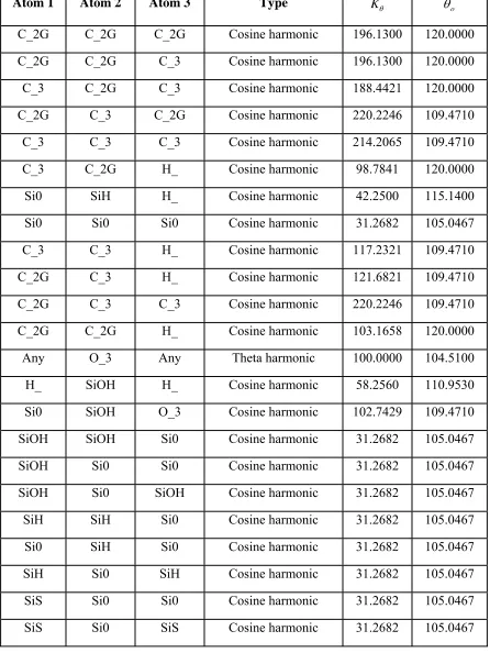
Energy Vs. Tip Postion Scan Point 9
45000 46000 47000
-1 0 1 2 3 4
Tip Position, nm
E n er g y , kca l/mo l
Force Vs. Tip Position Scan Point 9
-10 0 10 20 30 40
-1 0 1 2 3 4
Tip Position, nm
For
c
e
, nN
Energy Vs. Tip Position Scan Point 10
45000 46000 47000
-1 0 1 2 3 4
Tip Position, nm
E n er g y , kc al/ m o l
Force Vs. Tip Position Scan Point 10
-5 5 15 25 35
-1 0 1 2 3 4
Tip Position, nm
For
c
e
[image:35.612.117.518.71.347.2], nN
Figure S-1: Energy-distance and force-distance profiles generated for various probe positions,corresponding to the scan points in Figure 2 of the manuscript.
3. Effect of thermal vibrations
30 nN) did the probe “snap” off the sample nanotube at these points. The force and energy curves presented here show that the energy requirement to cause these points to snap is the same as that required to longitudinally compress the probe by one full nm, which is much greater than the available thermal energy. Our calculations show that the maximum horizontal displacement of any atom on the tip of the probe at 300 K is below 0.095 nm (less than 1.8% of the probe width), which would not significantly change the relative position of probe and sample. The amplitude of the vertical vibrations is less than 0.055 nm.
4. Characterization of SWNT deformation modes
31
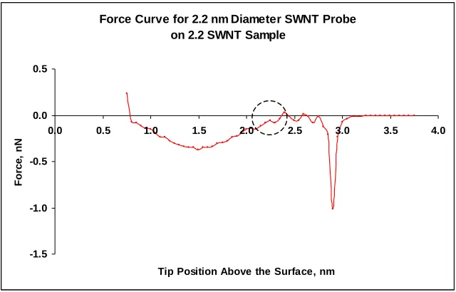
5. Slipping of smaller SWNT probes: 2.2 nm diameter, 20 nm in length
[image:37.612.114.539.160.433.2]32
Figure S-4: Force curve for the 2.2 nm SNWT probe. The dashed circle shows the region where slipping occurs. As the graph shows, there is no significant force opposing the snapping motion of the probe. The negative peak in the force is due to snap-to-contact as the probe first approaches the sample.
Force Curve for 2.2 nm Diameter SWNT Probe on 2.2 SWNT Sample
-1.5 -1.0 -0.5 0.0 0.5
0.0 0.5 1.0 1.5 2.0 2.5 3.0 3.5 4.0
Tip Position Above the Surface, nm
Fo
rc
e
[image:38.612.164.484.73.278.2]33 6. Illustration of reversibility in SWNT probe-sample interaction
34 required for geometry relaxation is on the order of 20 ps, one order of magnitude smaller than the integration time step used for AFM dynamics simulations (0.1 ns). This guarantees that the probe and sample are able to relax before the tip impacts the sample a second time.
REFERENCES:
1. Cheung, C-L; Hafner, J. H.; Odom, T. W.; Kyoungha, K.; Lieber, C. M. Appl. Phys. Lett. 2000, 76, 3136.
2. Wong, S. S.; Wooley, A. T.; Joselevich, E.; Cheung, C. L.; Lieber, C. M. J. Am. Chem. Soc. 1998, 120, 8557.
3. Campbell, P. M.; Snow, E. S.; Novak, J. P.; Appl. Phys. Lett. 2002, 81, 4586.
4. Hafner, J.H.; Cheung, C.L.; Oosterkamp, T.H.; Lieber, C.M.; J. Phys. Chem. B
2001, 105, 743.
5. Choi, N.; Uchihashi, T.; Nishijima, H.; Ishida, T.; Mizutani, W.; Akita, S.; Nakayama, Y.; Ishikawa, M.; Tokumoto, H.; Jpn. J. Appl. Phys. 2000, 39, 3707.
6. Dai, H.; Hafner, J.H.; Rinzler, A.G.; Colbert, D.T.; Smalley, R.E. Nature 1996, 384, 147.
35 8. Hafner, J. H.; Cheung, C. L.;. Wooley, A. T.; Lieber, C. M.; Progr. Biophys. Mol. Biol. 2001, 77, 73.
9. Stevens, R. M. D.; Frederick, N. A.; Smith, B. L.; Morse, D. E.; Stucky G. D.; Hansma P. K. Nanotechnology 2000, 11, 1.
10. Nguyen, C. V.; Stevens, R. M. D.; Barber, J.; Han, J.; Meyyapan, M. Appl. Phys. Lett. 2002, 81, 901.
11. Wade, L. A.; Shapiro, I. R.; Ma, Z.; Quake, S. R.; Collier, C. P. Nano Lett. 2004, 4, 725.
12. Snow, E. S.; Campbell, P. M.; Novak, J. P. Appl. Phys. Lett. 2002, 80, 2002.
13. García, R.; San Paulo, A. Phys. Rev. B. 1999, 60, 4961.
14. San Paulo, A.; García, R. Biophys. J. 2000, 78, 1599.
15. García, R.; San Paulo, A. Phys. Rev. B. 2000, 61, R13381.
16. San Paulo, A.; García, R. Phys. Rev. B. 2002, 66 041406(R).
17. San Paulo, A.; García, R. Phys. Rev. B. 2001, 64, 193411,
18. Frenkel, D.; Smit, B. Understanding Molecular Simulation; Academic Press: San Diego, CA, 2002, pp. 69-71.
19. For an explanation of (n,m) designation, see Jeroen, W. G.; Wildoer, L. C.; Venema, A. G.; Rinzler, R.; Smally, E.; Dekker, C. Nature 1998, 391, 59.
36 21. García, R.; Calleja, M.; Rohrer, H. J. Appl. Phys. 1999, 86, 1898.
22. Engel, A.; Müller, D. Nat. Struct. Biol. 2000, 7, 715.
23. Krishnan, A.; Dujardin, E.; Ebbesen T.W.; Yianilos, P.N.; Treacy, M. M. J. Phys. Rev. B
1998, 58, 14013.
24. Shen, W.; Jiang, B.; Han, B. S.; Xie, S-S. Phys. Rev. Lett. 2000, 84, 3634.
25. Gao, G.; Çağin, T.; Goddard, W.A. Nanotechnology 1998, 9, 184.
26. García, R.; Perez, R. Surf. Sci. Rep. 2002, 47, 197.
27. Lee, S. I.; Howell, S.W.; Raman, A.; Reifenberger, R. Phys. Rev. B. 2002, 66, 115409.
28. Wilson, N.R.; Macpherson, J.V. Nano Lett. 2003, 3, 1365.
29. Postma, H. W. C.; Sellmeijer, A.; Dekker, C. Adv. Mat. 2000, 12, 1299.
30. Hertel, T.; Walkup, R. E.; Avouris, P. Phys. Rev. B 1998, 58, 13870.
31. Li, C.; Chow, T-W.; Phys. Rev. B 2004, 69, 073401.
32. Ruoff, R.S.; Tersoff, J.; Lorents, D. C.; Subramoney, S.; Chan, B. Nature 1993, 364, 514.
33. Musgrave, C.B., 1995. PhD Dissertation Thesis: "Molecular Mechanics and ab
37 Semiconductor Superlattices, H Abstraction Tool for Nanotechnology, Polysilanes, and Growth of CVD Diamond" California Institute of Technology.
34. Guo, Y.J. 1992. PhD Dissertation Thesis: "Molecular Simulations of Buckyball Fullerenes. Quantum Chemistry Studies on High Tc Superconductors" California Institute of Technology.
35. Guo, Y.J.; Karasawan N.; Goddard W.A. III. Nature, 1991, 351, 6326.
38
Chapter 2: Mechanisms of Single-Walled Carbon Nanotube
Probe-Sample Multistability in Tapping Mode AFM Imaging
*ABSTRACT. When using single-walled carbon nanotube (SWNT) probes to create AFM images of SWNT samples in tapping mode, elastic deformations of the probe and sample result in a decrease in the apparent width of the sample. Here we show that there are two major mechanisms for this effect, smooth gliding and snapping, and compare their dynamics to the case when a conventional silicon tip is used to image a bare silicon surface. Using atomistic and continuum simulations, we analyze in detail the shape of the tip-sample interaction potential for three model cases and show that in the absence of adhesion and friction forces, more than two discrete, physically meaningful solutions of the oscillation amplitude are possible when snapping occurs (in contrast to the existence of one attractive and one repulsive solution for conventional silicon AFM tips). We present experimental results indicating that a continuum of amplitude solutions is possible when using SWNT tips and explain this phenomenon with dynamic simulations that explicitly include tip-sample adhesion and friction forces. We also provide simulation results of SWNT tips imaging Si(111)-CH3 surface step edges and Au
*
39 nanocrystals, which indicate that SWNT probe multistability may be a general phenomenon not limited to SWNT samples.
1. Introduction
Carbon nanotubes have been used successfully as AFM tips to image a variety of samples, including surfaces, biomolecules, and other types of nanoscale samples in both contact and non-contact mode. 1-7,9,10 These scanning probes have shown significant potential for numerous applications due to their robustness, flexibility, small dimensions, and chemical stability, which can lead to reduced sample damage and finer resolution imaging than can be obtained with conventional silicon tips. 2,3,8-10 SWNTs are of particular interest due to their macromolecular-scale dimensions.
Theoretical and experimental studies of AFM tapping-mode imaging have shown that this process is subject to bistability, i.e., it is possible to obtain two solutions of the AFM cantilever oscillation amplitude for a given set of imaging parameters. It has also been shown that there are cases where more than two solutions are mathematically possible but for which only two of them are physically meaningful. 11 Since the AFM imaging process in tapping mode depends on the oscillation amplitude of the cantilever, good images require that the regions where bistability occurs be avoided. Often there is no systematic procedure to do this, and AFM operators have to rely on their intuition and previous experience.
40 or negative. 11,12 In general, a typical tip-sample interaction potential contains a long-range attractive region and a short-long-range repulsive region, as do the well-known Morse and Lennard-Jones potentials, for example. The gradient of the tip-sample interaction force (negative of the second derivative of the potential with respect to the tip position) is positive in most of the attractive region and is negative in most of the repulsive region. If the region of positive force gradient dominates the tip-sample interaction for a given set of imaging parameters (attractive regime) the resulting phase shift of the AFM tip oscillation relative to the excitation force will be greater than 90º, and if the region of negative force gradient dominates (repulsive regime) the phase shift will be below 90º. 11,12
Note that throughout this paper we use the terms “phase” and “phase shift” interchangeably.
41 forces is different than the one described in references 11 and 12, where a single interaction potential gives rise to two different oscillation states).
Specifically, we analyze the tip-sample interaction potential of a SWNT AFM tip imaging a prone SWNT on a flat substrate. We have previously reported that for these systems it is possible to obtain a measured sample width that is smaller than the true sample width due to the elastic deformation of the tip and sample, which slide past one another. Here we show that this sliding phenomenon can occur in two different modes, one where the tip and sample glide smoothly past one another, and a second mode in which the tip initially compresses the sample and then snaps off, involving a sudden lateral “jump” to the side of the sample. In the absence of tip-sample adhesion and friction forces, the first mode gives rise to two amplitude solutions (as is typical with conventional silicon tips), and the second mode gives rise to four solutions due to the existence of two regions where the gradient of the tip-sample interaction force is positive and two regions where it is negative. In the presence of tip-sample adhesion and friction forces, these sliding phenomena can give rise to a continuum of amplitude solutions which exhibit smooth, continuous transitions between the attractive and repulsive regimes, in contrast to the discontinuities observed when using conventional silicon tips.
42 2. Methods
2.1 Experimental
The fabrication, characterization and imaging process employed using SWNT tips has been previously described. 6 A Digital Instruments§ (Santa Barbara, CA) Multimode atomic force microscope with a Nanoscope IV controller was used for this work. As-grown SWNTs were mounted onto silicon AFM tips (FESP, NanoWorld) using the pick-up technique developed by Lieber and coworkers.14 The experimental results presented here correspond to a SWNT AFM tip with diameter and length of approximately 5.5 and 40 nm, respectively, tilted 15 degrees with respect to the vertical direction (a transmission electron microscopy image of this probe6,13 is provided in the supporting information), mounted on a silicon tip with dimensions given in Table 1. These experimental results correspond to tapping-mode measurements for which the AFM tip was oscillating directly above the SWNT sample (a detailed procedure is provided in the supporting information). The relevant imaging and geometry parameters are listed in Table 1 and are the same as those used in the theoretical simulations. The cantilever driving frequency was the same as the resonance frequency in all cases.
§
43 2.2 Theoretical
The MD/AFMD simulation methodology has also been previously described (Chapter 1). 13 It consists of modeling the AFM cantilever tip as a point mass using the damped harmonic oscillator equation of motion with the introduction of tip-sample interaction forces obtained through atomistic simulations of tip and sample. Our tip-sample interaction potentials include both short- and long-range van der Waals interactions between each atom in the tip (both the SWNT and the supporting silicon tip) and the sample and substrate. The long-range interactions are introduced as a correction to the molecular simulation result via the Hamaker equation for an atom (for each atom in the SWNT tip) or a sphere (for the Si tip) interacting with the surface of a semi-infinite solid (MD calculations usually neglect long-range attractive interactions since they use cutoffs on the order of 1 nm in the calculation of van der Waals interactions).
The equation of motion for a damped harmonic oscillator is the following:
) cos( ) ( ) , ( ) , ( ) , ( 2 2 t F z F dt t Z dz Q m t Z kz dt t Z z d
m ts ts o
c o c
c =− − ω + + ω
, (1)
where z(Zc,t) is the instantaneous tip position with respect to its equilibrium rest position (Zc), k is the harmonic force constant for the displacement of the tip with respect to its equilibrium rest position, m is the AFM cantilever’s effective mass, ω0 = k/m is
44 F
0cos(ω t) is the oscillating driving force applied to the cantilever (we used ω = ωo as in our experiments). The oscillation amplitude is obtained directly from the tip trajectory. The phase is obtained from its Fourier transform. Our previous publication describes in detail the software and MD parameters used in the calculations. 13 The references for the MD parameters for Au nanocrystals and Si(111)-CH3 surfaces are provided in supporting information.
In this study we analyze three model cases in detail:
1) 17-nm-radius conventional silicon tip tapping on a bare silicon surface.
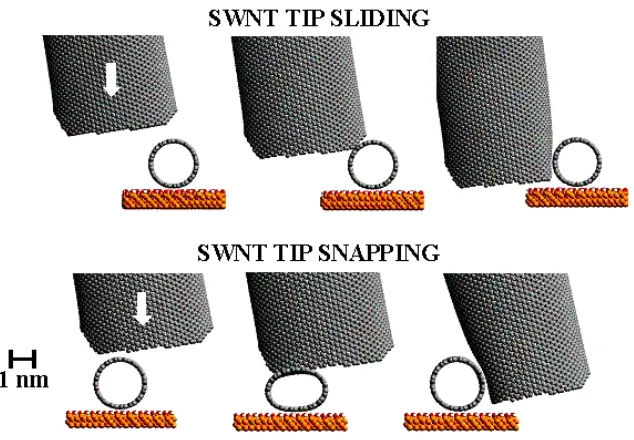
2) 40,40 SWNT tip tapping on the edge of a 16,16 SWNT sample, such that smooth gliding occurs when the probe descends on the sample as shown at the top of Figure 1.
3) 40,40 SWNT tip tapping on a 16,16 SWNT sample, such that the probe first compresses the sample and then snaps past it as shown at the bottom of Figure 1. Our analysis includes more than one variation of this case, depending on the magnitude of the force required for snapping to occur.
45 0.0025 nm/s, 0 nm/s, and -0.0025 nm/s. In all cases, the initial tip position was set equal to its equilibrium position, i.e., z(ZC,0)=0. These sets of data for each potential were used to construct the “phase space” representations of the oscillation amplitude solutions as a function of the variables Ao, Zc, and Vo.
Figure 1. 40,40 SWNT tip imaging a sample 16,16 SWNT in smooth gliding mode (top) and snapping mode (bottom). In the first case the deformation of the sample is negligible and the tip and sample are able to slide past one another primarily due to tip bending and local deformation. In the second case the sample nanotube is initially compressed against the substrate, undergoing elastic deformation until the tip snaps off the sample.
46 from the sample. The magnitude of this adhesive force was selected to be within the range given in the work of other authors.15-17
Table 1: Geometry and AFM simulation parameters Geometry parameters:
Silicon tip radius, imaging end 17 nm Silicon tip, base of pyramid 6800 nm
Silicon tip length 17500 nm
SWNT tip diameter 5.5 nm (simulated as a 40,40 SWNT)
SWNT tip length 40 nm
SWNT tip tilt angle 15 degrees
Sample SWNT diameter 2.1 nm (simulated as a 16,16 SWNT) Imaging parameters:
AFM cantilever force constant 4.8 N/m AFM cantilever resonant frequency 47.48 kHz AFM cantilever quality factor 150
Integration time step 0.1 ns
Integration time 0.02 s
Calculated cantilever effective mass 5.3933 x 10⁻¹¹ kg
47 they were in contact and sliding past one another. The effective quality factor, Q, was thus varied between these two values in the integration of Equation 1. There is no information available on the magnitude of these tip-sample friction forces during imaging, so we varied the contact quality factor between 0.005 and 0.05 times the free oscillation quality factor until we were able to reproduce the features observed in the experimental results (this is equivalent to assuming that for a given tip velocity, the tip-sample friction forces are between 20 and 200 times greater than the air damping forces experienced by the free oscillating cantilever). Our introduction of a tip-sample dissipation force proportional to the velocity is an approximation similar to that used in describing Newton’s law of viscosity for the case of two parallel plates sliding with respect to one another while a Newtonian fluid is being sheared between them. 20 The true nature of the tip-sample interaction forces between SWNT AFM tips and samples depends on atomistic phenomena that are different than those present in a continuum description of a Newtonian fluid and is expected to exhibit complex, non-monotonic behavior,21-24 but the results presented in the next section show that this model is able to reproduce the experimental results qualitatively.
48 3. Results
Figure 2 shows the tip-sample interaction force as a function of the tip position above the surface for the three model cases under study, in the absence of tip-sample adhesion and friction forces. Figure 2 (a) is the tip-sample interaction force curve for a conventional 17-nm-radius silicon tip imaging a bare silicon surface. It shows a well-defined long-range attractive region and a short-range repulsive region. Figure 2 (b), which corresponds to the SWNT smooth gliding mode, shows that the tip-sample interaction force exhibits a local (attractive) minimum just below 2.5 nm as the probe first approaches the sample. It remains slightly negative (attractive) as tip and sample slide past one another until a second minimum at approximately 0 nm is reached, after which it becomes repulsive and continues to increase monotonically with further downward displacement of the probe. Negative values of the tip position correspond to elastic deformations in the SWNT tip and the sample nanotube upon contact. Note that the tip-sample force remains slightly attractive as the probe and sample glide past one another even though they are both undergoing elastic deformation. MD simulations indicate that this is due to the favorable van der Waals interactions between their graphitic surfaces.
49 path it followed to compress the sample. However, if the probe compresses the sample with a force that exceeds 15 nN, it will snap off as shown at the bottom of Figure 1, and the force will immediately decrease to a value close to zero. The probe will continue its downward trajectory until it reaches the substrate surface, where it will initially experience a small attractive force and then an increasingly repulsive force. When the probe retracts it will follow a different trajectory than when it initially approached the sample (red line) because snapping only occurs when the probe is moving downward.
Note that the magnitude of the attractive force at the force curve minimum is several times greater for a conventional tip (Figure 2 (a)) than a SWNT tip (Figures 2 (b) and (c), and Figure 2-S of the supporting information). This is due to the greater number of atoms in the solid silicon tip, which experience strong van der Waals attractions with the substrate surface at short range. Even for the same tip radius, SWNTs have significantly fewer atoms in close proximity to the surface due to their hollow geometries, resulting in much smaller attractive forces.
20
-20
-1 1 2 3
20
-20
-1 1 2 3
20
-20
-1 1 2 3
SWNT Tip Sliding
SWNT Tip Snapping Silicon Tip
(a) (b) (c)
Ti p position, nm Ti p position, nm Ti p position, nm
F o rc e, n N F o rc e, n N F o rc e, n N Down Up 20 -20
-1 1 2 3
20
-20
-1 1 2 3
20
-20
-1 1 2 3
SWNT Tip Sliding
SWNT Tip Snapping Silicon Tip
(a) (b) (c)
Ti p position, nm Ti p position, nm Ti p position, nm
F o rc e, n N F o rc e, n N F o rc e, n N Down Up Down Up
50 curve for the SWNT tip imaging a bare silicon surface is similar to curve (b) and is shown in Figure 2-S of the supporting information.
52
Attractive, no snapping Repulsive, no snapping Attractive, snapping Repulsive, snapping
5 40 Cantilever Position, nm 5 40 A m pl it ude
, nm Attractive, no snapping
Repulsive, no snapping Attractive, snapping Repulsive, snapping Attractive, no snapping Repulsive, no snapping Attractive, snapping Repulsive, snapping
5 40 Cantilever Position, nm 5 40 A m pl it ude , nm 5 40 Cantilever Position, nm 5 40 A m pl it ude , nm
Figure 3. Ao-Zc phase space representation of the oscillation amplitude solutions for SWNT tip-sample interactions corresponding to Figure 2 (c) for V0 = 0, in the absence of tip-sample adhesion and friction forces. The corresponding phase space representations for V0 = -0.0025 nm/s and V0 = 0.0025 nm/s are qualitatively similar.
53 SNAPPED UNSNAPPED 40 0 20
0 25 50 0
90
45
25 50
Attractive
Repulsive
Cantilever position, nm Cantilever position, nm
P h a se, d eg rees A m p lit u d e, n m SNAPPED UNSNAPPED 40 0 20
0 25 50 0
90
45
25 50
Attractive
Repulsive
Cantilever position, nm Cantilever position, nm
P h a se, d eg rees A m p lit u d e, n m
Figure 4. Amplitude and phase vs. cantilever position for the SWNT tip-sample interaction in snapping mode in the absence of tip-sample adhesion and friction forces. The free oscillation amplitude A0 was 40 nm, and the initial tip velocity was set to zero in the simulation. The points where the tip snaps during every oscillation are shown in red, and those for which it does not snap are shown in blue. These curves were constructed using force curve (c) of Figure 2.
54 Figure 5 (c) shows that it is also possible to have smooth variations between the attractive and repulsive regimes and discontinuities on the same curve. The discontinuity of this curve, where the phase jumps from a value below 90º to a lower value, is similar to the jumps observed in Figure 4, indicating a transition between a regime where the probe snaps during each oscillation (henceforth referred to as a snapped oscillation) to a regime where the probe does not snap during the oscillation (henceforth referred to as an unsnapped oscillation) as the cantilever equilibrium position, Zc, is lowered. The relative magnitude of the phase between the snapped and unsnapped oscillations is consistent with Figure 4, which shows that the phase is higher for snapped oscillations than for unsnapped oscillations. This is also consistent with the magnitude of the oscillation amplitude before and after the jump, which indicates that the oscillation amplitude is greater when snapping occurs. The amplitude curve shows two transitions, one from an unsnapped oscillation to a snapped oscillation and one from a snapped oscillation back to an unsnapped oscillation. Although the first transition is not as evident in the phase curve, this curve has an inflection point which indicates a change in the nature of the tip-sample interaction.
We also observed curves with similar behavior to that of a conventional silicon tip, although the range of Zc corresponding to the attractive region was generally much larger. In general, the experimental measurements show significantly greater attractive regions than those calculated based on van der Waals interactions alone, suggesting the presence of other attractive interactions such as capillary or electrostatic forces.
55 in the theoretical methods section. All three simulated phase curves in Figure 6 are in close qualitative agreement with their experimental counterparts in Figure 5, although the transitions in the experimental amplitude curves in Figure 5 are more pronounced than in the corresponding simulations (see discussion below Figure 6). The curves in Figure 6 (a), which were constructed using the force curve of Figure 2 (c), indicate that the tip did not snap during the oscillation until the separation distance to the surface was nearly zero (indicated by the sharp minimum in the phase curve when Zc approaches zero) and that the predominantly attractive region is a consequence of the large tip-sample adhesion and frictional components that were included in the tip-sample interaction.
56
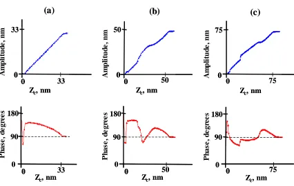
Figure 5. Experimental amplitude and phase vs. Zc for a SWNT tip tapping directly on top of a sample SWNT on a silicon oxide substrate for different values of the free oscillation amplitude (A0): (a) A0=33 nm, (b) A0=50 nm, (c) A0=75 nm.
The simulations show that as the tip-sample friction forces increase (i.e. as Qc is lowered), the transitions between attractive and repulsive regimes become smoother because the larger friction forces allow the probe to more gradually approach and move away from the sample during every oscillation, which causes the average tip-sample interaction force to vary smoothly from positive to negative and vice-versa.
The phase curve of Figure 6 (c) is similar to that of Figure 5 (c) except that it shows both snapping transitions clearly. This simulation was performed using different values of the friction and adhesion forces for snapped and unsnapped oscillations. The maximum of the adhesion force was set to 20 nN for unsnapped oscillations and to 5 nN
33
0
0 33 0 50 0 75
0 33 0 50 0 75
0
0 0 0
90
0 180
0 0 0
(c) (b) (a) P h as e , d e gr ee s A m pl it ud e , nm 50 0 0 90 0 180 P h as e , d e gr ee s A m pl it ud e , nm 75 0 0 90 0 180 P h a se , d e g re e s A m pl it ud e , nm
Zc, nm Zc, nm
Zc, nm
Zc, nm Zc, nm
Zc, nm 33
0
0 33 0 50 0 75
0 33 0 50 0 75
0
0 0 0
90
0 180
0 0 0
(c) (b) (a) P h as e , d e gr ee s A m pl it ud e , nm 50 0 0 90 0 180 P h as e , d e gr ee s A m pl it ud e , nm 75 0 0 90 0 180 P h a se , d e g re e s A m pl it ud e , nm
Zc, nm Zc, nm
Zc, nm
Zc, nm Zc, nm
57 for snapped oscillations (this is reasonable since MD simulations show that the tip-sample contact area is significantly smaller after the tip snaps). The contact quality factor for snapped oscillations was set to 90% of the value for unsnapped oscillations.
33
0
0 33 0 50 0 75
0 33 0 50 0 75
0
0 0 0
90
0 180
0 0 0
(c) (b) (a) P h as e , d e g re e s A m pl it ud e , n m 50 0 0 90 0 180 P h as e , d e gr ee s A m pl it u d e , n m 75 0 0 90 0 180 P h a se , d e g re e s A m pl it ud e , nm
Zc, nm Zc, nm
Zc, nm
Zc, nm Zc, nm
Zc, nm 33
0
0 33 0 50 0 75
0 33 0 50 0 75
0
0 0 0
90
0 180
0 0 0
(c) (b) (a) P h as e , d e g re e s A m pl it ud e , n m 50 0 0 90 0 180 P h as e , d e gr ee s A m pl it u d e , n m 75 0 0 90 0 180 P h a se , d e g re e s A m pl it ud e , nm
Zc, nm Zc, nm
Zc, nm
Zc, nm Zc, nm
[image:63.612.113.539.168.426.2]Zc, nm
Figure 6. Simulated amplitude and phase vs. Zc for snapping potentials with the inclusion of adhesion and friction forces for different values of the free oscillation amplitude (A0): (a) A0=33 nm, (b) A0=50 nm, and (c) A0=75 nm. We have included straight dotted lines for easier visualization of the curvature of the amplitude curves. The adhesion and friction force parameters are provided in the supporting information.
Figure
Related documents