Structural Dynamics of GaN
Microcrystals in Evolutionary Selection
Selective Area Growth probed by X-ray
Microdiffraction
V. Kachkanov1, B. Leung2, J. Song2, Y. Zhang2, M.-C. Tsai2, G. Yuan2, J. Han2& K. P. O’Donnell3
1Diamond Light Source Ltd, Diamond House, Chilton, Didcot, Oxfordshire, OX11 0DE, UK,2Department of Electrical Engineering, Yale University, 15 Prospect St, New Haven, CT, 06511, USA,3Department of Physics, SUPA, University of Strathclyde, Glasgow, Scotland, G4 0NG, UK.
A method to grow high quality, single crystalline semiconductor material irrespective of the substrate would allow a cost-effective improvement to functionality and performance of optoelectronic devices. Recently, a novel type of substrate-insensitive growth process called Evolutionary Selection Selective Area Growth (ES-SAG) has been proposed. Here we report the use of X-ray microdiffraction to study the structural properties of GaN microcrystals grown by ES-SAG. Utilizing high resolution in both direct and reciprocal spaces, we have unraveled structural dynamics of GaN microcrystals in growth structures of different dimensions. It has been found that the geometric proportions of the growth constrictions play an important role: 2.6mm and 4.5mm wide growth tunnels favor the evolutionary selection mechanism, contrary to the case of 8.6mm growth tunnels. It was also found that GaN microcrystal ensembles are dominated by slight tensile strain irrespective of growth tunnel shape.
T
he development of modern electronics industry relies heavily upon processes designed to produce semi-conductor materials in the form of thin films. Epitaxial growth has been a mainstay of the semisemi-conductor industry, enabling fabrication of electronic devices for a wide range of applications1. However, a fun-damental requirement of epitaxial growth is the availability of crystalline substrates lattice-matched to the material of the film; when this is not realized, lattice mismatch becomes a major obstacle, deteriorating the crystalline quality of epitaxial layers through the introduction of strain and defects2,3. To circumvent the lattice-matching requirement it was suggested to use artificially patterned amorphous or polycrystalline substrates for deposition4,5. The ability to grow single crystalline semiconductor material on an amorphous surface would allow a selection of functional substrates to complement or improve the functionality of devices. For example, the use of transparent and/or flexible substrates for GaN-based Light Emitting Diodes (LEDs), or thermally and electrically conductive metal foil substrates for electrical devices, can be realised. Recently, some of the present authors reported a novel type of substrate-insensitive growth process named as Evolutionary Selection Selective Area Growth (ES-SAG)6. The ES-SAG process is based on a mechanism defined as evolutionary selection7whereby the fastest-growing crystal grains overtake their slower neighbors and become dominant; an engineered growth constrictionfilters misaligned grains thus forming a polycrystalline layer into a nearly monocrystalline one. The process, depicted in Fig. 1, utilizes lithographic techniques and selective area growth. A typical growth sequence consists of two stages, and within each stage the ES principle will reduce the degrees of freedom in orientation. The first stage is the deposition of an AlN film, with a preferred orientation set by the ES principle in the direction perpendicular to the substrate surface. Then, a SiO2dielectric structure is fabricated to confine growth in two dimensions. Subsequent growth on the previously defined textured seed, through the confined structure, will allow the number of grains of the growing material, originally nucleated on the seed, to be reduced in a direction parallel to the substrate surface. However, to understand the ES-SAG process fully requires a spatially resolving characterization technique that can assess both strain and structural quality of the material of interest on the microscale.X-ray diffraction is a very sensitive and non-invasive structural tool. Recent advances in X-ray optics have lead to the development of various micro- and nanofocusing optical elements8. The use of focused X-ray beams brings
OPEN
SUBJECT AREAS:
ELECTRONIC DEVICES CHARACTERIZATION AND ANALYTICAL TECHNIQUES STRUCTURE OF SOLIDS AND LIQUIDS DESIGN, SYNTHESIS AND PROCESSING
Received 6 September 2013 Accepted 26 March 2014 Published 11 April 2014
spatial resolution to diffraction analysis, thereby increasing the func-tionality of the technique9,10. In this work we report the investigation of growth dynamics of GaN microcrystals in ES-SAG using high-resolution X-ray microdiffraction in three dimensions.
Results
Fig. 2 shows representative Scanning Electron Microscopy (SEM) images of the sample studied. As the proposed idea assumes that numerous crystallites nucleate on the AlN seed, the GaN/AlN inter-face is shown magnified in Figs. 2 (d),(e) and (f). It is seen that voids in the material form lines which propagate from the AlN seed along the growth direction. This is a first indication that GaN microcrystals form during growth, with the voids defining their boundaries. Further along the growth direction, for the narrower channels, the
voids disappear, while for the wider channels, they can propagate through the entire length of the tunnel. Characterization by Electron Backscatter Diffraction (EBSD) indicates that lateral growth through the tunnel structure enables an evolutionary selection process to take place, resulting in a large single-crystal GaN on the completely cov-ered SiO2substrate surface6. EBSD also shows that initially nucleated
GaN grains are randomly oriented in-plane but follow the (0001) texture of the AlN seed. However, the angular resolution of the EBSD setup was no better than,1 degree; thus a technique with higher angular resolution is required for detailed characterization of quality and strain state of GaN microcrystals.
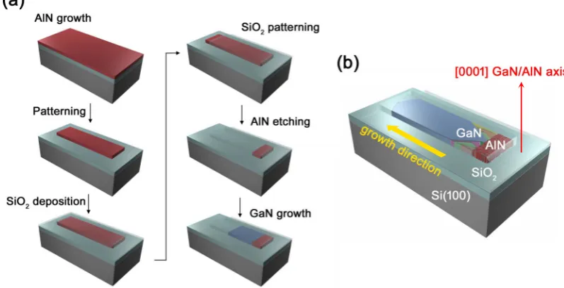
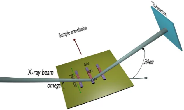
[image:2.595.96.495.59.263.2]The concept of the X-ray microdiffraction experiment is depicted in Fig. 3. The focused X-ray beam probed structural properties of GaN microcrystals in the growth tunnels. The angle of incidencev Figure 1|Fabrication and concept of Evolutionary Selection Selective Area Growth.(a) processing steps for fabrication of SiO2growth tunnels; (b)
[image:2.595.124.475.467.709.2]Schematics of the ES process in the growth tunnel: GaN microcrystals retain the (0001) texture of the AlN seed while randomly oriented in-plane.
Figure 2|Top view SEM images of GaN crystals grown by ES-SAG.(a) 2.6mm, (b) 4.5mm, and (c) 8.6mm wide growth tunnels. The SiO2tunnel
confined mask structure has been removed by buffered oxide etch to expose the GaN and AlN seed, as well as the Si(100) substrate. Scale bar is 10mm. Magnified view of the GaN/AlN interface is shown in (d), (e) and (f) for representative 2.6 mm, 4.5 mm and 8.6 mm wide grown GaN.
was scanned around the (0002) reflection of GaN with an area detector positioned at the expected2hangle. The footprint of the focused X-ray beam on the sample was,3.4314.0mm FWHM for the (0002) reflection. The sample was oriented in such a way that the longest dimension of the X-ray beam was perpendicular to the growth direction. Maxima of intensity are observed when the Bragg condition is satisfied for individual microcrystals. On the area detector the position of a diffraction peak can be used to calculate the absolute modulus of the scattering vector Q; the width of a diffraction peak on the area detector is equivalent to a rocking curve scan, i.e. it is indicative of crystalline quality. The experiment resem-bles a powder diffraction experiment with (0002) reflections from
individualgrains arranged in a partial Debye-Scherrer ring; partial since there is a preferential orientation set by the AlN growth ‘‘seed’’. The accuracy of the experiment is estimated to be60.0003 A˚21along the [0002] direction in reciprocal space. Note that each microcrystal can be identified by its unique coordinates in the 3D angular space: viz. the incidence angle and two position coordinates on the area detector. The focused X-ray spotenhancesmicrocrystal identifica-tion by limiting the number probed at any one time. The divergence of the incident beam does not degrade the resolution in reciprocal space since each microcrystal acts as a tiny analyzer crystal thereby reducing the angular spread of the diffracted X-ray beam on the area detector. No correlation was found between the intensities and the broadening of X-ray diffraction peaks, suggesting that due to short integration times (1–2 sec) the measurements were not sensitive to grains small enough for the Scherrer equation to play a substantial role.
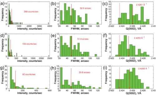
Fig. 4 shows the statistical distribution of intensity, the crystalline quality (indicated by the FWHM distribution of diffraction peaks) and the modulus of the scattering vector, Q(0002), for microcrystals grown in tunnels of three different widths. Four growth tunnels of each width were probed along the growth direction. For the statistical analysis for each probed growth tunnel a single vscan with the highest intensity was selected to avoid double counting of microcrys-tals. Figs. 4(a), (d), (g) show microcrystal intensity distributions for tunnels of different width. The intensity of the X-ray diffraction peaks is proportional to the volume of the microcrystals and it is used here as a guide to their size. A typical intensity distribution has a tail of high intensity peaks corresponding to relatively large micro-crystals; average intensity is 268 counts/sec, 159 counts/sec and 92 counts/sec for 8.6mm, 4.5mm and 2.6mm wide tunnels, respect-ively. Therefore on average GaN microcrystals are biggest in the
8.6mm wide tunnels and smallest in the 2.6mm wide tunnels as we might expect. Figs. 4(b), (e), (h) show the distribution of X-ray diffraction peak FWHMs for microcrystals in growth tunnels of different width. Generally, FWHM distributions are broad with a lower limit defined by the detector resolution of 23 arcsec and an upper limit reaching 130 arcsec. Average FWHM is 52.0 arcsec, 51.9 arcsec and 50.8 arcsec for 8.6mm, 4.5mm and 2.6mm wide tunnels, respectively. For reference, these values of crystalline quality are about a tenth of the FWHM reported for GaN on Si substrates11, a third of that typical of HVPE grown GaN12and three times larger than that of the best bulk GaN substrates13.
Figs. 4(c), (f), (i) show the distributions of Q(0002). The average values of Q(0002) are 2.4261 A˚21, 2.4253 A˚21and 2.4255 A˚21which correspond to tensile strains of 0.10%, 0.07% and 0.08% for micro-crystals in 8.6mm, 4.5mm and 2.6mm tunnels, respectively. In unstrained GaN the c lattice constant value is 5.1850 A˚14 which corresponds to a Q(0002) of 2.4236 A˚21; any deviation from this value indicates the presence of strain in a microcrystal. It is imme-diately obvious that, for the majority of microcrystals, the Q(0002) values are higher than what is expected for strain-free GaN. Assuming that elasticity theory is valid, it is an indication of the tensile strain dominating microcrystal ensembles irrespective of the growth tunnel geometry. In other words,clattice parameter is compressed on average while a lattice parameters are stretched. However, it is not possible to deduce the direction of the biaxial strain from a symmetric reflection.
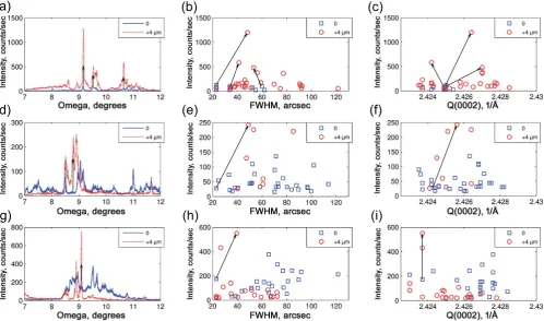
[image:3.595.142.458.53.243.2]Fig. 5 compares X-ray diffraction measured along the growth direction for tunnels of different geometry. Utilizing the spatial reso-lution provided by a microfocused X-ray beam, two regions in the growth tunnels were probed: one close to the GaN/AlN interface and another 4mm further along the growth direction. This separation is close to three times standard deviation of the beam size and thus there is no overlap between the two probed volumes. The structural comparison of these two regions reveals the dynamics of the growth process for GaN microcrystals in ES-SAG. Figs. 5(a), (d), (g) show the dependence of maximal intensity registered by the detector as a function of incidence anglev. Figs. 5(b), (e), (h) and Figs. 5(c), (f), (i) compare the dynamics of crystalline quality and strain state of GaN microcrystals for tunnels of different width. It is immediately noticeable that the growth dynamics in 8.6mm growth tunnel is different from that in 4.5mm and 2.6mm tunnels. In 8.6mm tunnels, there are more GaN microcrystals further away from the interface and they are biggerat the same time. The average FWHM actually
Figure 3|Schematics illustrating microdiffraction experiment.Focused X-ray beam has been used to probe GaN microcrystals in growth tunnels. The sample was mounted on the diffractometer x-y translation stage in such a way that the longest dimension of the X-ray beam was perpendicular to the growth direction.
increases from 38.5 arcsec to 57.1 arcsec and the average tensile strain increases from 0.05% to 0.09%. The structural dynamics changes completely in narrower growth tunnels. GaN microcrystals become bigger as their number decreases. The average crystalline quality improves from 64.2 arcsec to 56.7 arcsec and from 65.1 arc-sec to 45.1 arcarc-sec for 4.5 and 2.6mm tunnels respectively. Regarding the average strain state, the tensile strain relaxes from 0.09% to 0.07% and from 0.12% to 0.06% for 4.5 and 2.6mm tunnels respectively. The trend of tensile strain relaxation and improvement of crystalline quality is more pronounced for the narrowest 2.6mm growth tunnel. Simultaneous increase of the size and number of microcrystals in the case of 8.6mm tunnels cannot be explained by the peculiar triangular shape of the GaN/AlN interface as shown on Fig. 2(f). For narrower growth tunnels, the volume of probed material is also higher further from the GaN/AlN interface, since roughly half of the X-ray beam falls on AlN when the beam is on the interface. However, adecreasein the number of grains is still observed as the volume of material probedincreases. This is the key indication that evolutionary selec-tion is taking place in 4.5 and 2.6mm tunnels but not in 8.6mm tunnels.
Since each microcrystal can be uniquely identified by its location in 3D angular space, it is possible to trace the evolution of an indi-vidual microcrystal along the growth direction and such an analysis is shown in Fig. 5 for some of the largest examples as we are interested only in those that survive and grow during ES-SAG. Three large microcrystals can be traced back to the start of growth in the 8.6mm growth tunnel. Remarkably, the strain state evolution for the three largest microcrystals points to a common initial tensile strain of,0.06%. Only a single microcrystal can be traced back in both the 4.5mm and 2.6mm growth tunnels. Note that the largest microcrystal in the 2.6mm growth tunnel incorporates no additional strain as it grows.
Discussion
Evolutionary selection is the key principle of the ES-SAG process and it is based on competition between crystal grains during growth. The dependence of the structural dynamics of GaN microcrystals on the growth tunnel width indicates that the geometric proportions of the growth constrictions play an important role; at the same time point-ing to the spatial scale on which evolutionary selection takes place. The growth dynamics in 4.5mm and 2.6mm tunnels conforms to the idea of evolutionary selection. The best outcome in terms of crystal-line quality and strain state of GaN microcrystals is observed for the narrowest 2.6mm growth tunnels. On the other hand, the growth dynamics in the widest 8.6mm growth tunnels does not show selec-tion of microcrystals; instead it is their diversificaselec-tion that is uniquely observed in these high-resolution studies which reveal the growth dynamics of spatially traceable individual microcrystals.
[image:4.595.50.551.51.358.2]Another interesting observation is that GaN microcrystal ensem-bles are always grown with slight tensile strain. This tensile strain is a manifestation of residual stress in the microcrystals. It is worth not-ing that the material system under investigation shares more sim-ilarity with polycrystalline thin films than with epitaxial layers. A lot of work has been devoted to investigations of intrinsic residual stress in polycrystalline metallic thin films15–19. It is generally assumed that the residual stress can be classified into three main components: intrinsic, thermal and external. Formation of grain boundaries dur-ing coalescence of grains was first suggested as a mechanism for generation of intrinsic residual stress15. Later, a quantitative evalu-ation of the intrinsic residual stress was proposed based on size-dependent phase transition of nanograins19,20. In this model it is assumed that the phase transition from liquid to solid induces a volume change due to thermal contraction that leads to intrinsic residual stress. Thermal residual stress is caused by the difference in thermal expansion coefficients between the film and the substrate,
Figure 4|Statistical distibution of intensity, FWHM and modulus of scattering vector Q(0002) for X-ray diffraction peaks of GaN microcrystals.
8.6mm (a), (b), (c), 4.5mm (d), (e), (f) and 2.6mm (g), (h), (i) wide growth tunnels. The average values are indicated by red arrows. In (c), (f), (i) dashed red arrows indicate Q(0002) values for strain-free GaN.
whereas the main cause of external residual stress is the oxidation and incorporation of impurities. For GaN on SiO2, thermal stress can
be ruled out since as it would lead to tensile strain values,0.5%, higher than the observed values. The extrinsic stress due to diffusion of aluminium atoms and oxidation can also be ruled out as GaN growth is carried out after etching of previously grown AlN and GaN is not susceptible to oxidation under normal conditions. The only viable explanation for tensile strain is the intrinsic stress. Interestingly, for thin metallic films it was shown that intrinsic resid-ual stress is generally tensile and contributes significantly more to the overall stress in comparison to thermal stress15,17,18. We suggest that the observed strain, which dominates the microcrystal ensembles, originates from intrinsic residual stress generated in microcrystals during ES-SAG. Assuming that residual stress is biaxial and isotropic in the basal plane it is possible to estimate residual stress using elastic theory21:
ec~{2E{1sv, ð1Þ
whereecis the strain component along thec-axis,sis biaxial stress,E
is Young’s modulus andnis Poisson’s ratio. Using reported values for Poisson ration<0.2321and Youngs’modulusE5330 GPa22, the tensile strain of 0.10% would correspond to residual stress s<
0.72 GPa. However, the full understanding of intrinsic residual stress in ES-SAG requires detailed modeling similar to that done in Ref. 19, 20. It is the key to the further development and application of this novel growth method.
Methods
Evolutionary Selection Selective Area Growth.GaN growth on SiO2was performed
by the ES-SAG method. The processing steps for ES-SAG are shown in Fig. 1. A textured (0001) AlN film, 0.65mm thick, was deposited by rf-magnetron sputtering
on a SiO2-covered Si(100) wafer. The AlN is patterned by standard photolithography
and reactive-ion etching into 15mm long stripes with widths of 2.6mm, 4.5mm and
8.6mm. Plasma-enhanced chemical vapor deposition (PECVD) of 800 nm SiO2was
then performed to cover the AlN stripes. In a second photolithography step, SiO2was
removed on the sides of the AlN patterns by a buffered oxide etch. AlN is then etched back using 25% tetramethylammoniumhydroxide (TMAH) at 65uC. Note that the thickness of the AlN film defines a vertical size for growth tunnels. After substrates were cleaned thoroughly, they were loaded in a metal-organic chemical vapor deposition (MOCVD) system for GaN growth. Trimethylgallium (TMGa) and ammonia (NH3) were used as sources for gallium and nitrogen, respectively, and H2
as a carrier gas. TMGa is introduced at a temperature of 1030uC, 300 mbar, and 0.5 slm NH3. Typical longitudinal growth rates of GaN inside the tunnels are 7–12mm/h.
The determination of the length scales for growth tunnels was based on the spatial scale where evolutionary selection is taking place. Importantly, the length and the width of the tunnels required to reduce the polycrystallinity scale with the nuclei density, which has been experimentally observed to be,2–43104cm21for GaN on AlN in our MOCVD growth conditions. In order to have an effect in a reasonable growth time, this sets an upper bound of,10mm on the width of tunnel that should be used for the ES process. The minimum bound is given by practical considerations, as only conventional photolithography is used, in which structures,2mm in size are easily fabricated. An intermediate width is chosen for comparison. The exact widths of the structures deviate slightly from design due to process conditions (over/under exposure) during the photolithography, yielding our current measured widths.
X-ray microdiffraction in three dimensions.The microdiffraction experiments were carried out on beamline B16 at the Diamond Light Source, UK. The X-ray energy was fixed at 12400 eV (1 A˚ ). The X-ray beam was focused by a Beryllium Compound Refractive Lens (CRL) comprising 63 individual components. The focused X-ray beam size was,3.4 (horizontal)mm32.4mm (vertical) full width at half maximum (FWHM). The horizontal and vertical incident beam divergences were
,0.8 mrad. The required sample rotations and translations were performed using a high precision 5-circle Huber diffractometer with 0.1 millidegree resolution and a Huber XYZ sample stage with 0.5mm resolution. A Pilatus 300k detector with pixel size of 0.17230.172 mm was used to record 2D X-ray diffraction patterns.
[image:5.595.51.550.53.347.2]The addition of an area detector to a 5-circle diffractometer makes the setup effectively a 6-circle diffractometer23. In order to calculate the components of the scattering vector in the diffractometer frame of reference the following equations have been used:
Figure 5|Structural evolution of GaN microcrystals along the growth direction.8.6mm (a), (b), (c), 4.5mm (d), (e), (f) and 2.6mm (g), (h), (i) wide growth tunnels. The first probed area close to the GaN/AlN interface is compared to a second one which is 4mm further along the growth direction. In (b), (e), (h) the average FWHM changes from 38.5 to 57.1 arcsec, from 64.2 arcsec to 56.7 arcsec, and from 65.1 arcsec to 45.1 arcsec, respectively. In (c), (f), (i) the average Q(0002) changes from 2.4248 A˚21to 2.4258 A˚21, 2.4257 A˚21to 2.4253 A˚21, and 2.4265 A˚21to 2.4251 A˚21. The black arrows trace the evolution of individual microcrystals. The accuracy of the experiment in reciprocal space is estimated to be60.0003 A˚21.
Qx~2p
lðcosd|cosc{1Þ, ð2Þ
Qy~
2p
lcosd|cosc, ð3Þ
Qz~
2p
lsind, ð4Þ
wheredis the angle between the detector arm and the horizontal plane,cis the angle between the detector arm and the vertical plane23. It is worth noting thatdis not the same as the Bragg angle2hwhich forms the Debye-Scherrer rings on a detector. The angular resolution of the detector, defined by pixel size and detector-sample distance, was,23 arcsec giving overall angular span of,3.9uforcand,3.1uford.
In the microdiffraction experiment, the incidence anglevis scanned while area detector is fixed at expected2hangle. When the incidence angle matches the Bragg conditions for a microcrystal, an X-ray diffraction spot is observed on 2D detector producing a peak in incidence anglevversus maximal intensity plot i.ev-scan. For clarification, maximal intensity is maximal intensity in a single pixel and not the intensity integrated across all the pixels of the area detector. A broadening of an X-ray diffraction spot along2h(i.e. across the Debye-Scherrer ring) on the 2D detector indicates a spread of lattice parameter. The broadening perpendicular to2h, i.e. tangential to the Debye-Scherrer ring, also known asx-spread, is in this case a complex function of strain and orientation of unit cellsinside a single graini.e. crystal deformation.
To extract statistics on GaN grains in growth tunnels, peak positions inv-scans were extracted using a local maxima finding algorithm which utilizes first derivative test and Savitzky-Golay filtering for noise rejection. Thus a 2D image corresponding to a peak inv-scan was extracted and analyzed. The 2D image analysis was done in the following way:
1) Each pixel position in the image was converted into diffractometer anglesdand
cusing simple geometric relations.
2) Angular coordinates of the X-ray diffraction peak were used to calculate the absolute modulus of the total scattering vector Q using relations (2)–(4). 3) The line broadening indicated by FWHM was extracted by fitting each X-ray
diffraction peak with a Lorentzian along the2hdirection using standard non-linear least squares fit routine.
The MATLAB computing environment was used to carry out data analysis.
1. Stringfellow, G. B.Organometallic Vapor-Phase Epitaxy: Theory and Practice (Academic Press, 2nd ed., 1999).
2. Beanland, R., Dunstan, D. J. & Goodhew, P. J. Plastic relaxation and relaxed buffer layers for semiconductor epitaxy.Adv. Phys.45, 87–146 (1996).
3. Liu, L. & Edgar, J. H. Substrates for gallium nitride epitaxy.Mater. Sci. Eng. R37, 61–127 (2002).
4. Geis, M. W., Flanders, D. C. & Smith, H. I. Crystallographic orientation of silicon on an amorphous substrate using an artificial surface-relief grating and laser crystallization.Appl. Phys. Lett.35, 71–74 (1979).
5. Givargizov, E. I. Mechanisms of oriented crystallization in artificial epitaxy (graphoepitaxy).Thin Solid Films189, 389–396 (1990).
6. Leung, B., Song, J., Zhang, Y. & Han, J. Evolutionary selection growth: towards template-insensitive preparation of single-crystal layers.Adv. Mater.25, 1285; DOI: 10.1002/adma.201204047(2013).
7. van der Drift, A. Evolutionary selection, a principle governing growth orientation in vapour-deposited layers.Philips Res. Rep.22, 267–288 (1967).
8. Sakdinawat, A. & Attwood, D. Nanoscale X-ray imaging.Nature Photon.4, 840–848 (2010).
9. Kachkanov, V.et al. InGaN epilayer characterization by microfocused x-ray reciprocal space mapping.Appl. Phys. Lett.99, 181909-12181909-3 (2011).
10. Kachkanov, V.et al. Characterisation of III-nitride materials by synchrotron X-ray microdiffraction reciprocal space mapping.Phys. Stat. Sol. (c)10, 481;DOI: 10.1002/pssc.201200596(2013).
11. Drechsel, P.et al. Impact of buffer growth on crystalline quality of GaN grown on Si(111) substrates.Phys. Stat. Sol. (a)209, 427–430 (2012).
12. Sato, T.et al. Free-standing GaN wafer by one-stop HVPE with pit-induced buffer layer.Phys. Stat. Sol. (c)10, 359;DOI: 10.1002/pssc.201200535(2013). 13. Dwilin´ski, R.et al. Bulk ammonothermal GaN.J. Cryst. Growth311, 3015–3018
(2009).
14. Detchprohm, T., Hiramatsu, K., Itoh, K. & Akasaki, I. Relaxation process of the thermal strain in the GaN/a-Al2O3heterostructure and determination of the
intrinsic lattice constants of GaN free from the strain.Jpn. J. Appl. Phys.31, L1454–L1456 (1992).
15. Murbach, H. P. & Wilman, H. The origin of stress in metal layers condensed from the vapour in high vacuum.Proc. Phys. Soc. B66, 905–911 (1953).
16. Hoffman, R. W. Stresses in thin films: relevance of grain boundaries and impurities.Thin Solid Films34, 185–190 (1976).
17. Koch, P. & Abermann, R. On the influence of thermal effects on internal stress measurements during and after deposition of silver, gold and copper films.Thin Solid Films129, 63–70 (1985).
18. Koch, P. & Abermann, R. Microstructural changes in vapour-deposited silver, copper and gold films investigated by internal stress measurements.Thin Solid Films140, 217–226 (1986).
19. Guisbiers, G., Van Overschelde, O. & Wautelet, M. Nanoparticulate origin of intrinsic residual stress in thin films.Acta Mater.55, 3541–3546 (2007). 20. Guisbiers, G. & Wautelet, M. Size, shape and stress effects on the melting
temperature of nano-polyhedral grains on a substrate.Nanotechnology17, 2008–2011 (2006).
21. Kisielowski, C.et al. Strain-related phenomena in GaN thin films.Phys. Rev. B54, 17745–17753 (1996).
22. Yang, Z.et al. Mechanical characterization of suspended GaN microstructures fabricated by GaN-on-patterned-silicon technique.Appl. Phys. Lett.88, 041913 (2006).
23. Lohmeier, M. & Vlieg, E. Angle calculations for a six-circle surface X-ray diffractometer.J. Appl. Cryst.26, 706–716 (1993).
Acknowledgments
Diamond Light Source is acknowledged for providing beamtime. The material growth research was supported by the U.S. Department of Energy, Office of Basic Energy Sciences, Division of Materials Sciences and Engineering under Award #DE-SC0001134.
Author contributions
V.K. carried out the microdiffraction experiment and data analysis. B.L., J.S., Y.Z., M.-C.T., G.Y. and J.H. grew the sample. V.K. wrote the paper with suggestions from K.P.O’D. and B.L.
Additional information
Competing financial interests:The authors declare no competing financial interests.
How to cite this article:Kachkanov, V.et al. Structural Dynamics of GaN Microcrystals in Evolutionary Selection Selective Area Growth probed by X-ray Microdiffraction.Sci. Rep.4, 4651; DOI:10.1038/srep04651 (2014).
This work is licensed under a Creative Commons Attribution 3.0 Unported License. The images in this article are included in the article’s Creative Commons license, unless indicated otherwise in the image credit; if the image is not included under the Creative Commons license, users will need to obtain permission from the license holder in order to reproduce the image. To view a copy of this license, visit http://creativecommons.org/licenses/by/3.0/