Authors’ Accepted Manuscript version of Journal of Applied Physics, vol. 116, article 044512
Size-dependent capacitance study on InGaN-based micro-light-emitting diodes Wei Yang,1,a Shuailong Zhang,2,3,a Jonathan J. D. McKendry,2 Johannes Herrnsdorf,2 Pengfei Tian,2 Zheng Gong,2,b Qingbin Ji,1 Ian M. Watson,2 Erdan Gu,2,3,c Martin D. Dawson,2 Liefeng Feng,4 Cunda Wang,1,4 and Xiaodong Hu1,c
1. State Key Laboratory for Artificial Microstructure and Mesoscopic
Physics, School of Physics, Peking University, Beijing 100871, China
2. Institute of Photonics, SUPA, University of Strathclyde, Glasgow G4 0NW, UK
3. Joint Laboratory of Advanced Optoelectronic Materials and Devices,
State Key Laboratory, Wuhan University of Technology, China and Institute of Photonics, University of Strathclyde, Glasgow G4 0NW, UK 4. Department of Applied Physics, Tianjin University, Tianjin, 300072,
China
a)Wei Yang and Shuailong Zhang contributed equally to this work.
b) Current address: mLED Ltd., Glasgow G1 1XN, United Kingdom.
c) Email: [email protected]; [email protected]
We report a detailed study on size-dependent capacitance, especially the negative capacitance (NC), in InGaN-based micro-pixelated light-emitting diodes (µLEDs).
I. INTRODUCTION
In contradiction to Shockley’s model and conventional p-n junction theory,1
abnormal negative capacitance (NC) has been observed repeatedly in alternating current (AC) impedance measurements of many semiconductor devices such as light-emitting diodes (LEDs), laser diodes and quantum well infrared photo-detectors.2-10 The capacitance of a semiconductor device is usually extracted from the imaginary part of the complex impedance under direct current (DC) biased AC impedance measurements. When the transient current caused by the small modulation signal lags behind the modulation voltage, capacitance with negative values is obtained from the device under test.2 NC has the same phase relationship between small-modulation-signal voltage and transient current as a positive inductance, however, the interpretation of NC as conventional inductance or conventional capacitance with negative values is not physically meaningful.2 Until now, the general physical explanation of NC effect in semiconductor devices is still under debate.4,5,9-11
Thus far, all LEDs used for NC studies have focused on conventional broad-area devices, which are mainly developed for solid-state lighting (SSL),12 and have typical emission areas ranging from 300×300 µm2 to 1 mm2. However, NC of micro-pixelated LEDs (µLEDs),13,14 which have typical sizes of several tens of microns or less, has not been investigated before. Due to a reduction in device
performance in many aspects, such as their modulation bandwidth,20 the size effect on LED NC should be investigated in detail.
In this work, we present, for the first time, a systematic study of the size-dependent capacitance in InGaN-based µLEDs under reverse and large forward bias, based on AC impedance measurements. µLED clusters consisting of uniform-sized µLED pixels were chosen for the study instead of individual µLED pixels with different sizes, because among the latter the current spreading is quite different as the pixel size changes.15,21 Each µLED pixel is 40×40 µm2, which is also
the smallest tested LED. By inter-connecting the basic µLED pixels (sharing p and n
contacts) into square n×n clusters (n = 1,…,10), µLED clusters with device areas
ranging from 40×40 to 400×400 µm2 are formed. In these cluster devices, we observed a linear relationship between the capacitance and their sizes under reverse bias and low forward bias. However, a slight deviation from this linear relationship was observed for NC under high forward bias. Furthermore, to study how the device format and fabrication process affect the capacitance, two broad-area LEDs with the same total area as two typical µLED clusters were also fabricated. The µLED cluster devices showed a stronger NC effect compared with the two reference broad-area devices which are attributed to defects brought by the sidewall damage. These results shed light on the mechanisms underlying the NC effect.
II. LED WAFER EPITAXIAL GROWTH, DEVICE FABRICATION AND
CHARACTERIZATION METHOD
The µLED cluster arrays reported here are made from a 450 nm-emitting wafer grown on c-plane sapphire substrate by metal organic chemical vapour deposition. Its epitaxial structure begins with a 1.5-µm-thick GaN buffer layer followed by a 4-µm-thick Si-doped n-type GaN layer. Then the active region was grown, which is made up by an eleven-pair In0.16Ga0.84N (2.8 nm)/GaN (13.5 nm)
multi-quantum-well (MQW) layer. After that, a 30-nm-thick p-AlGaN
electron-blocking layer (EBL) was grown on top of the active region. Finally, a 160-nm-thick Mg-doped p-type GaN layer was grown on top of the EBL.
evaporator for Ni/Au (10 nm/20 nm) spreading metal deposition. Cluster arrays of different pixel numbers were then formed by aqua-regia wet etching Ni/Au using lithography-defined photoresist pattern as a mask, followed by inductively coupled plasma (ICP) dry etching down to n-GaN. Thus Ni/Au spreading metal was formed on each pixel in a self-aligned fashion, simplifying the fabrication procedure. P-type Ohmic contacts were then formed by annealing the spreading metal (on each pixel) at 500 ºC for 2 minutes under purified air. The next step was to form a common
n-contact for the µLED clusters by sputtering Ti/Au (50 nm/200 nm). The common
n-contact was designed to surround each µLED cluster, in order to ensure uniform current injection. The following step was to deposit a 200-nm-thick SiO2 layer by
plasma-enhanced chemical vapour deposition. Then a SiO2 aperture on each pixel was
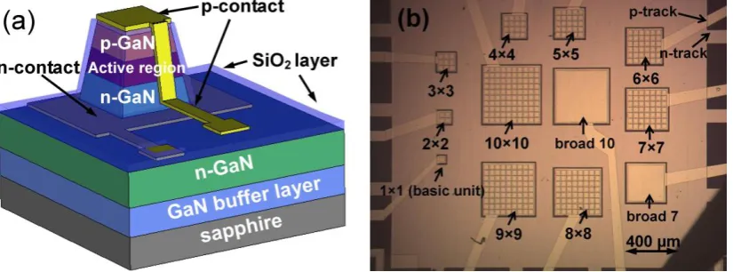
formed by ICP dry etching, followed by buffered oxide etch (BOE). It was found that if only the BOE was used, the Ni/Au spreading metal might be degraded by long-term exposure to BOE. Finally, independent p-metal track (50 nm Ti/ 200 nm Au) was formed to interconnect all pixels in each µLED cluster device, so that each interconnected cluster could be individually addressed. For comparison purposes, two square-shaped broad-area LEDs were also fabricated on the same chip. Each has the same total area as the 7×7 and 10×10 µLED clusters, and is marked as “broad 7-square” and “broad 10-square” respectively. Fig.1 (a) shows a 3D schematic of a typical pixel that forms the µLED clusters. Fig.1 (b) shows a top-view optical microscope image of a chip with different LED devices, providing more specific information about the structure and layout of the fabricated devices.
[image:4.595.95.508.532.685.2]
The current-voltage (I-V) and capacitance-voltage (C-V) characteristics of LEDs were measured by a probe station connected to an Agilent 4155C semiconductor parameter analyzer and an Agilent 4294A precision impedance analyzer respectively. The C-V characteristics were measured under a small modulation signal with an oscillation level of 50 mV and a frequency of 100 kHz. The equivalent circuit model of LED for measuring C-V can be found in our previous publications.5-8 Light output power was measured by putting a silicon photo-detector of a calibrated power-meter on top of the emitting surface of each LED device.
III. RESULTS AND DISCUSSIONS
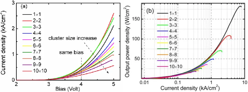
FIG. 2: (a) characteristics of current density versus applied bias of µLED cluster devices with different sizes; (b) semi-logarithmic plot of power density versus current density for µLED cluster devices.
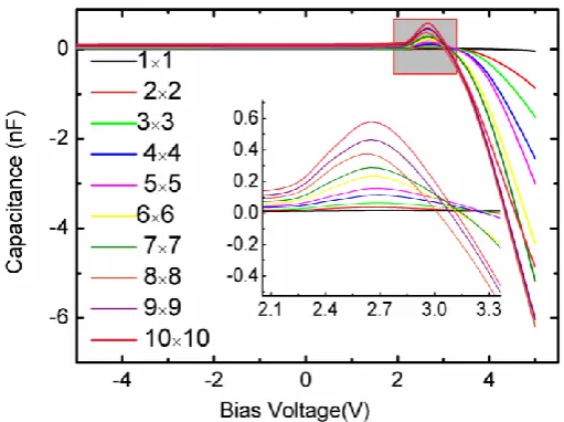
Fig.3 shows the capacitance spectroscopy of µLED cluster devices with applied
voltage changing from -5 V to +5 V. The capacitance of all µLED clusters, no matter their size, shows similar trends: the value of capacitance is positive under reverse bias; then increases with forward bias to a peak (the peak area is enlarged and shown in the inset of Fig. 3); after that, it decreases with further increasing forward bias and drops down to a negative value. Similar trends have been widely observed in conventional broad-area LED devices,6-8 proving that both µLEDs and broad-area LEDs are dominated by same physical mechanism, no matter the size and format of the device. This trend of capacitance with the increase of bias can be explained as follows. Under reverse bias, the width of the depletion region and the carrier concentration in the depletion region change with the applied bias, and the capacitance of device is dominated by the depletion capacitance. Under forward bias, a lot of carriers will pass through the depletion region and the depletion approximation is no longer applicable. In this case, the carriers that are stored in either the n-type or p-type diffusion region change with the applied bias and this capacitance effect is known as the diffusion capacitance. In conventional p-n junction theory,1 the forward capacitance is dominated by diffusion capacitance and should increase exponentially with bias voltage. However, the experimental results are contradictory to those predicted by Shockley’s theory, as a capacitance peak is observed and then it drops down to
negative value. Hence, there should be a NC mechanism that shows opposite trend to
diffusion capacitance and increases much faster with forward bias. According to Ershov et al.,2 who interpreted the NC effect based on the measuring principle, NC is
[image:6.595.94.503.73.225.2]transient current in response to a small voltage step. This interpretation is very persuasive in numerically charactrizing the appearance of NC, but less insightful in clarifying the underlying physical mechanism,which is particularly interesting for NC
[image:7.595.171.427.179.370.2]research.
FIG. 3: C-V characteristics of µLED clusters with different sizes, the inset shows an enlarged picture of the capacitance peaks in shaded area.
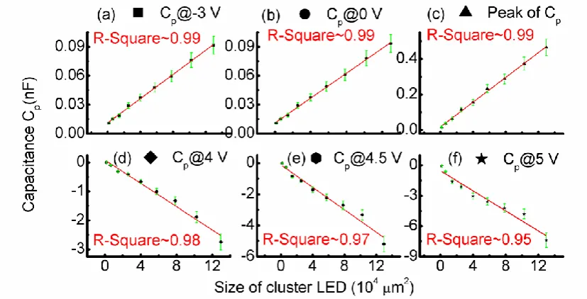
Fig. 4 shows the size-dependent capacitances at different bias voltages for µLED cluster devices. Depletion capacitance, geometrical capacitance (capacitance at 0 V) and the peak capacitance are all plotted against device sizes in Fig. 4(a), (b), and (c). Corresponding plots in the NC regime at +4 to +5 V are shown in Figs. 4 (d) ~ (f). The size effect on NC under forward bias is of practical interest because all the devices are turned on at +4 V and the devices have a high injection current density at +5 V. Linear fitting of capacitance with size is indicated by red-solid lines for all the data. Very good linear relationships are observed for depletion capacitance, geometrical capacitance and the peak capacitance (R-squared~0.99). As mentioned above, under reverse bias and low forward bias (V<kBT/qe, kB is Boltzmann constant, T is temperature and qe is elementary charge), the capacitance of LED are dominated
FIG. 4: Size-dependent (a) depletion capacitance (capacitance at -3 V), (b)
geometrical capacitance (capacitance at 0 V), (c) the peak of diffusion capacitance and NC at (d) +4 V,(e) +4.5 V and (f) +5 V of cluster devices. Linear fitting of
capacitance with LED size is shown in red-solid line for all the data, together with the R-square for each fitting.
However, different from the conventional depletion and diffusion capacitance, the data points of size-dependent NC show a systematic deviation (although relatively small) from linearity with the increase of applied bias, as illustrated in Figs.4 (d) ~ (f). Since the cluster devices are made from parallel-interconnected uniform µLED pixel, the capacitance of the clusters is the sum of capacitance of each single pixel. If each µLED pixel has the same NC response under same driving conditions, then the NC of the µLED cluster should scale linearly with the number of µLED pixels and its own size. However, the linear relationship between NC and device size is degraded under large forward bias, in contradiction to normal sense. To clarify this abnormal relationship between NC and the device size, we investigated the normalized capacitance, i.e. the capacitance per device area, as a function of the applied bias for different µLED cluster devices. Fig.5 (a) shows the characteristics of normalized capacitance versus bias voltage of different µLED cluster devices. The curves of normalized capacitance of different clusters overlap well under low forward bias but show a systematic trend of deviation to each other with the increase of forward bias.
[image:8.595.91.505.71.282.2]bias, causing the linearity deviation observed in Fig.4 (d) ~ (f). To further explain the observed experimental results, normalized capacitances of µLED cluster devices are plotted as a function of injection current density and shown in Fig.5 (b). According to previous investigations and theoretical interpretation, NC effect is closely related to injected carriers and carrier dynamics.8-10 If we assume the NC effect of µLED cluster devices is dominated by the same carrier mechanism, then the normalized NC of µLED cluster devices should behave similarly under the same injection current density. As shown in Fig.5 (b), the normalized NCs of different µLED clusters show
similar trends with the increase of current density and the variation of normalized NCs is smaller than the variation of normalized NCs shown in Fig.5 (a). Further analysis
suggests that the observed small differences on normalized NCs of µLED cluster devices under the same current densities is probably due to their different junction temperatures.15,22 As mentioned above, larger µLED clusters are less competitive in thermal management and subsequently affected more by the self-heating effect. A further measurement of junction temperature by spectral shift method shows that the junction temperature of a larger-size µLED cluster is higher than that of a smaller-size µLED cluster under the same current densities. Fig. 6 shows the C-V characteristics of a 5×5 cluster device with an ambient temperature increasing from 26 °C (room temperature) to about 200 °C. A clear increase of the NC effect can be seen and a similar trend was observed in other cluster devices as well. Therefore, different junction temperatures in different µLED clusters can cause the variation of normalized NC values when they are driven under the same injection current densities. Temperature-dependent NC characteristics of broad-area LEDs have been investigated before and physical explanation of the results observed in Fig.6 has been proposed.23 Although the normalized NC of smaller µLED cluster device is smaller than that of the larger µLED cluster device under the same injection current density, the smaller µLED cluster device is able to be driven at higher current densities compared with the larger µLED cluster device, which allows the maximum NC value
FIG. 5 (a) characteristics of normalized capacitance versus forward bias of µLED
cluster devices; (b) characteristics of normalized capacitance versus current density of µLED cluster devices.
FIG. 6: Temperature-dependent C-V of 5×5 cluster device. The inset is NC as a function of temperature under a forward bias of +4 V and +5 V respectively.
[image:10.595.185.409.72.399.2] [image:10.595.191.403.476.637.2]device under the same bias, causing the linearity deviation between NC and device size. These results indicate that the NC of LEDs measured at a fixed applied bias should not be used directly to characterize the size effect as the NC of LEDs is a current/carrier-dependent phenomenon and is essentially different from the conventional capacitance. Therefore, current-dependent NC characteristics are more insightful than widely-reported voltage-dependent NC characteristics for the NC research. In addition, different from conventional depletion and diffusion capacitances, the normalized NC of these µLED cluster device is also influenced by other factors,
such as self-heating effect. It will also be interesting to relate these findings to other characteristics of µLEDs, such as modulation bandwidth. The high modulation
bandwidths of µLEDs in excess of 400 MHz have been demonstrated.20 This fast modulation response occurs in a regime of high NC, i.e. the µLEDs are operated at high injection current densities. The investigation on the relationship of these characteristics is underway and our findings will be reported in due course.
To further study the influence of device format and the relevant fabrication process to NC and shed light on the underlying physics, Fig. 7 compares the capacitances of the 7×7 and 10×10 µLED cluster devices and two broad-area devices with the same total area. Due to the small pixel separation (2 µm) between µLED pixels that form the cluster devices, the cluster device and the broad-area device with the same total area are influenced by similar self-heating effect under the same applied bias, indicated by their similar optical performances under CW operation. In addition, the I-V characteristics of the cluster device and the broad-area device with the same total area are quite similar, indicating the injection current densities in both the cluster device and broad-area device are similar under the same applied bias. The capacitances of these LED devices from -1 V to +1 V is enlarged and shown in the inset of Fig. 7. From the enlarged picture, the cluster devices and broad-area devices with the same total size have very close values of capacitance. This phenomenon is well understood because both depletion capacitance and diffusion capacitance should
induced sidewall damage compared with the broad-area LEDs due to different sidewall area to volume ratios. The sidewall damage can bring more sub-band gap defects to the device, resulting in an increase of population and depopulation of trap states by carriers on the sidewall surface of LED. Therefore, the ICP-etching induced sidewall defects can increase the sub-band gap defect density and the amount of trapped states significantly, which according to the Bansal-Datta-theory corresponds to a stronger NC effect in cluster µLEDs.
FIG. 7: C-V characteristics of µLED clusters and broad-area LEDs with same total area and inset shows enlarged picture of capacitance from -1 to +1 V.
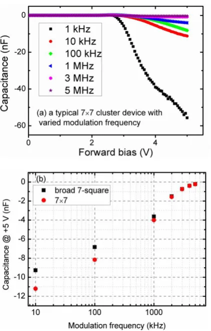
To provide further evidence for the above interpretation, we measured the C-V characteristics of 7×7 µLED cluster device and its broad-area counterpart under different modulation frequencies. In Fig. 7(a), the capacitances of a typical 7×7 cluster device with modulation frequency varied from 1 kHz to 5 MHz are shown. Under the same forward bias (> 2.5 V), µLED cluster device shows a decreasing value of NC (absolute value) with increasing modulation frequency. In the Bansal-Datta-model,9 the carriers from sub-band gap defects can not follow the change of a high-frequency modulation signal and will be trapped at the sub-band gap defects due to finite inertia. This explanation can be verified after comparing the NC value of µLED cluster device with that of broad LED device. As shown in Fig.7 (b), with the increase of modulation frequency, the difference of NC value between µLED cluster device and broad-area LEDs becomes smaller and smaller at the same forward bias of +5 V. The reason is that more carriers in the sub-band gap defects are trapped and no longer able to participate in any recombination process. Therefore, under high
[image:12.595.190.402.223.389.2]functional and the NC of µLED cluster device approaches the value of broad-area counterpart.
FIG. 8: (a) Typical C-V characteristics of a 7×7 cluster device with modulation frequency varied from 1 kHz to 5 MHz; (b) comparison between NC of 7×7 µLED cluster and broad-area LED at different modulation frequencies under +5 V applied bias.
IV. CONCLUSIONS
[image:13.595.193.404.115.445.2]voltage. This view is well-aligned with theories that NC is an effect of carrier dynamics and/or occupation of certain states (e.g. sub-bandgap states). Compared to broad-area devices with same total area, µLED clusters have a similar depletion capacitance and diffusion capacitance but larger value of NC than their broad-area counterparts at large forward bias. A possible reason may be from the extra sub-band gap states contributed from the sidewall defects in µLED clusters induced by ICP etching damage. By investigating the size-dependent capacitance of InGaN-based µLEDs, this research provides insight into the mechanism underlying the NC effect
observed in LED devices.
ACKNOWLEDGEMENTS
The work was supported by the National Natural Science Foundation of China (Grants No. DMR-11204209, 61076013 and 51272008), Beijing Municipal Science
and Technology Project (No. H030430020000), UK EPSRC (Grant No. EP/K00042X/1) and the National Basic Research Program of China under Grants No. 2012CB619304 and No. 2012CB619306. Wei Yang and Qingbin Ji acknowledge the support from UK EPSRC for their visit to University of Strathclyde under the project “Global - Promoting Research Partnerships: Strathclyde Escalator for Global
Engagements in Research” (Grants No. EP/K004670/1).
References
1 S. M. Sze and K. K. Ng, Physics of Semiconductor Devices. (John Wiley &Sons, 2006), p. 80-102.
2 M. Ershov, H. C. Liu, L. Li, M. Buchanan, Z. R. Wasilewski, and A. K. Jonscher, IEEE Trans. Electron Dev. 45, 2196 (1998).
3 J. Werner, A. F. J. Levi, R. T. Tung, M. Anzlowar, and M. Pinto, Phys. Rev. Lett. 60, 53 (1988).
4 A. G. U. Perera, W. Z. Shen, M. Ershov, H. C. Liu, M. Buchanan, and W. J. Schaff, Appl. Phys. Lett. 74, 3167 (1999).
5 C. D. Wang, C. Y. Zhu, G. Y. Zhang, J. Shen, and L. Li, IEEE Trans. Electron Devices 50, 1145 (2003).
6 L. F. Feng, Y. Li, C. Y. Zhu, H. X. Cong, and C. D. Wang, IEEE J. Quant. Electron. 46, 1072 (2010).
7 Y. Li, C. D. Wang, L. F. Feng, C. Y. Zhu, H. X. Cong, D. Li, and G. Y. Zhang, J. Appl. Phys. 109, 124506 (2011).
8 L. F. Feng, Y. Li, D. Li, X. D. Hu, W. Yang, C. D. Wang, and Q. Y. Xing, Appl. Phys. Lett. 101, 233506 (2012).
10 C. Y. Zhu, L. F. Feng, C. D. Wang, H. X. Cong, G. Y. Zhang, Z. J. Yang, and Z. Z. Chen, Solid-State Electron. 53, 324 (2009).
11 J. Shulman, Y. Y. Xue, S. Tsui, F. Chen, and C. W. Chu, Phys. Rev. B 80, 134202 (2009).
12 S. Pimputkar, J. S. Speck, S. P. DenBaars, and S. Nakamura, Nat Photon 3, 180 (2009).
13 Z. Y. Fan, J. Y. Lin, and H. X. Jiang, J. Phys. D: Appl. Phys. 41, 094001 (2008).
14 H. X. Jiang, and J. Y. Lin, Opt. Express 21, 475 (2013).
15 Z. Gong, S. Jin, Y. Chen, J. J. D. McKendry, D. Massoubre, I. M. Watson, E. Gu, and M. D. Dawson, J. Appl. Phys. 107, 013103 (2010).
16 S. Zhang, Z. Gong, J. J. D. McKendry, S. Watson, A. Cogman, E. Xie, P. Tian, E. Gu, Z. Chen, G. Zhang, A. E. Kelly, R. K. Henderson, and M. D. Dawson, IEEE Photonics Journal 4, 1639 (2012).
17 S. Zhang, S. Watson, J. J. D. McKendry, D. Massoubre, A. Cogman, E. Gu, R. K. Henderson, A. E. Kelly, and M. D. Dawson, IEEE J. Lightwave Technol. 31, 1211 (2013).
18 N. McAlinden, D. Massoubre, E. Richardson, E. Gu, S. Sakata, M. D. Dawson, and K. Mathieson, Opt. Lett. 38, 992 (2013).
19 A. H. Jeorrett, S. L. Neale, D. Massoubre, E. Gu, R. K. Henderson, O. Millington, K. Mathieson, and M. D. Dawson, Opt. Express 22, 1372 (2014). 20 J. J. D. McKendry, D. Massoubre, S. Zhang, B. R. Rae, R. P. Green, E. Gu, R.
K. Henderson, A. E. Kelly, and M. D. Dawson, IEEE J. Lightwave Technol. 30, 61 (2012).
21 P. Tian, J. J. D. McKendry, Z. Gong, B. Guilhabert, I. M. Watson, E. Gu, Z. Chen, G. Zhang, and M. D. Dawson, Appl. Phys. Lett. 101, 231110 (2012). 22 N. Lobo Ploch, H. Rodriguez, C. Stölmacker, M. Hoppe, M. Lapeyrade, J.