Theses
7-2019
Exploration of GPU Cache Architectures Targeting
Machine Learning Applications
Gerald Kotas
[email protected]Follow this and additional works at:https://scholarworks.rit.edu/theses
This Thesis is brought to you for free and open access by RIT Scholar Works. It has been accepted for inclusion in Theses by an authorized administrator of RIT Scholar Works. For more information, please [email protected].
Recommended Citation
GERALD KOTAS July 2019
A Thesis Submitted in Partial Fulfillment
of the Requirements for the Degree of Master of Science
in
Computer Engineering
GERALD KOTAS
Committee Approval:
Dr. Sonia L´opez Alarc´onAdvisor Date RIT, Department of Computer Engineering
Dr. Marcin Łukowiak Date
RIT, Department of Computer Engineering
Dr. Roy Melton Date
First and foremost, I would like to thank my advisor Dr. Sonia L´opez Alarc´on for her
guidance and support throughout this entire process. This has been a long and arduous
process and I am thankful for all of the help along the way. I would also like to thank Dr.
Marcin Łukowiak and Dr. Roy Melton for serving on my thesis committee.
Next, I want to thank my friends for continually pushing me and driving me in the right
direction. Finally, I would like to thank my family for their support and understanding for
The computation power from graphics processing units (GPUs) has become prevalent in
many fields of computer engineering. Massively parallel workloads and large data set
ca-pabilities make GPUs an essential asset in tackling today’s computationally intensive
prob-lems. One field that benefited greatly with the introduction of GPUs is machine learning.
Many applications of machine learning use algorithms that show a significant speedup on a
GPU compared to other processors due to the massively parallel nature of the problem set.
The existing cache architecture, however, may not be ideal for these applications. The goal
of this thesis is to determine if a cache architecture for the GPU can be redesigned to better
fit the needs of this increasingly popular field of computer engineering.
This work uses a cycle accurate GPU simulator, Multi2Sim, to analyze NVIDIA GPU
architectures. The architectures are based on the Kepler series, but the flexibility of the
simulator allows for emulation of newer features. Changes have been made to source code
to expand on the metrics recorded to further the understanding of the cache architecture.
Two suites of benchmarks were used: one for general purpose algorithms and another for
machine learning. Running the benchmarks with various cache configurations led to
in-sight into the effects the cache architecture had on each of them. Analysis of the results
shows that the cache architecture, while beneficial to the general purpose algorithms, does
not need to be as complex for machine learning algorithms. A large contributor to the
complexity is the cache coherence protocol used by GPUs. Due to the high spacial
local-ity associated with machine learning problems, the overhead needed by implementing the
coherence protocol has little benefit, and simplifying the architecture can lead to smaller,
Signature Sheet i
Acknowledgments ii
Abstract iii
Table of Contents iv
List of Figures vi
List of Tables 1
1 Introduction 2
1.1 Motivation . . . 3
2 Background 4 2.1 GPU Architectures . . . 4
2.2 Cache Architecture . . . 8
2.2.1 Cache Replacement Policies . . . 8
2.2.2 Cache Write Policies . . . 9
2.2.3 Cache Coherence Protocols . . . 11
2.3 Related Work . . . 25
3 Methodology 30 3.1 Multi2Sim . . . 30
3.1.1 Kepler Architecture . . . 31
3.1.2 Limitations and Modifications . . . 34
3.2 Benchmarks . . . 38
3.2.1 General Purpose . . . 38
3.2.2 Machine Learning . . . 40
4 Results and Analysis 44 4.1 Varying L2 Cache . . . 44
4.1.1 L1 Cache Size . . . 57
4.3 Varying Input Data Size . . . 65
4.4 Spatial Locality Benchmark . . . 69
5 Conclusions and Future Work 73
5.1 Conclusion . . . 73
5.2 Future Work . . . 75
2.1 CPU vs GPU Architecture [1] . . . 6
2.2 Performance Regions of a Unified Many-Core Many-Thread Machine . . . 7
2.3 State Transition Diagram for NMOESI Cache Coherence Protocol . . . 21
3.1 Block Diagram of the Memory Hierarchy of NVIDIA’s Kepler Architecture 33 4.1 Varying L2 Cache Size L2 Hit Ratios (16 KB L1 and 16-way L2) . . . 46
4.2 Varying L2 Cache Size L1 Hit Ratios (16 KB L1 and 16-way L2) . . . 48
4.3 Varying L2 Cache Size Simulation Times (16 KB L1 and 16-way L2) . . . 52
4.4 Varying L2 Cache Size Simulation Speedup (16 KB L1 and 16-way L2) . . 53
4.5 Varying L2 Cache Size Average Simulation Speedup (16 KB L1 and 16-way L2) . . . 55
4.6 Varying L2 Cache Size L2 Hit Ratios (16 KB L1 and 16-way L2) . . . 55
4.7 Varying L2 Cache Size L1 Hit Ratios (16 KB L1 and 16-way L2) . . . 56
4.8 Varying L2 Cache Size L2 Hit Ratio (16 KB and 32 KB L1 and 16-way L2) 58 4.9 Varying L2 Cache Size L1 Hit Ratio (16 KB and 32 KB L1 and 16-way L2) 58 4.10 Varying L2 Cache Size Simulation Speedup (16 KB and 32 KB L1 and 16-way L2) . . . 59
4.11 Varying Input Data Size L1 Hit Ratios . . . 66
4.12 Varying Input Data Size L2 Hit Ratios . . . 67
4.13 Varying Input Data Size Simulation Times . . . 68
4.14 Spatial Locality Benchmark L2 Hit Ratios (16 KB L1) . . . 70
4.15 Spatial Locality Benchmark L1 Hit Ratios (16 KB L1) . . . 71
4.16 Spatial Locality Benchmark Simulation Time (16 KB L1) . . . 71
1 Event Diagrams for Memory Access Handlers for the NMOESI Protocol as Implemented in Multi2Sim . . . 81
2 Event Diagrams for Internal Events for the NMOESI Protocol as Imple-mented in Multi2Sim . . . 83
2.1 MSI Cache Coherence Example . . . 12
2.2 MESI Cache Coherence Example . . . 14
2.3 State Definitions for NMOESI Protocol . . . 16
2.4 Transition Actions in the NMOESI Protocol . . . 18
2.5 State Transitions for NMOESI Protocol [2] . . . 20
2.6 NMOESI Cache Coherence Example 2 . . . 23
3.1 Default Module Characteristics for Kepler’s Memory Hierarchy . . . 32
3.2 Comparison of Various NVIDIA Architectures . . . 33
3.3 Coherence Matrix Origin Identifier Descriptions . . . 37
3.4 List of General Purpose Benchmarks . . . 39
3.5 List of Machine Learning Benchmarks . . . 42
4.1 Coherence Matrix Origin Identifier Descriptions . . . 60
4.2 Cache Coherence Matrices for L1 Cache from Transpose Benchmark . . . . 62
4.3 Cache Coherence Matrices for L1 Cache from Histogram Benchmark . . . 64
Introduction
Graphics processing units (GPUs) may have started out as dedicated processors to handle
the graphics of a computer, but they have evolved to a much more critical role. Computing
and displaying intricate graphics is major application for GPUs; however, general purpose
computing has become an increasingly popular application ever since NVIDIA introduced
CUDA, its general purpose application programming interface (API) [3]. These general
purpose GPUs, known as GPGPUs, use the CUDA development environment to integrate
with the central processing unit (CPU) of a computer. This integration of two different
types of processors is the basis of heterogeneous computing.
Heterogeneous computing is the idea that multiple different processor types work
to-gether as a single system. This is powerful because it leverages the fact the different
pro-cessors excel at their own types of target applications. When multiple different propro-cessors
are available, the best processor for the job is selected, and the best performance can be
achieved for many different problems. GPUs are a key component to almost all
heteroge-neous systems due to their unique ability to handle massively parallel problems in a very
efficient manner. Today’s problems all deal with massive amounts of data that need to be
processed, making the GPU a viable option for many of the cutting edge applications. This
1.1
Motivation
A large and ever-growing field in computer engineering is machine learning. The nature
of machine learning applications is large data and parallel execution. These characteristics
point to GPUs being a practical option when choosing which processor to use. The
motiva-tion of this work is to focus on the cache performance of the GPU when executing machine
learning algorithms. Since GPUs are designed to handle a wide variety of problem types,
the specific use case of machine learning may not be getting all of the performance speedup
that could be possible, or the architecture has unneeded resources that add to the production
or running cost.
The GPU cache architecture was modeled after that of the CPU, with slight
modifi-cations. The work of this research involves running many general purpose and machine
learning benchmarks on various different cache configurations. By analyzing the results,
an alternative cache architecture may be found that suits machine learning applications
better than the general purpose one that already exists in GPUs.
This research gets its foundation from the work of Nimkar in [4]. He created a suite
of machine learning benchmarks to simulate the workload of actual machine learning
ap-plications. Since the GPU simulator cannot run full machine learning programs, a set of
common algorithms used by a wide variety of machine learning applications were
com-piled. This suite was used in his work which found that there was different cache behavior
when compared to the general purpose benchmark suite. Nimkar found that the L2 cache
hit ratio is always low, around 50%. He also found that the most recently used cache line
accounts for a majority of the hits leading to the conclusion that a large L2 cache isn’t
nec-essary for machine learning applications. The work of this thesis dives more into the reason
why this is the case and reconfigures the cache architecture to better suit the machine
learn-ing benchmarks. An area of focus is the L2 cache due to its large size in manufacturlearn-ing and
Background
2.1
GPU Architectures
The architecture of a GPU differs greatly from that of the conventional CPU. This
alter-native architecture is what allows for the massively parallel abilities of the GPU. The two
main producers of GPUs are NVIDIA and AMD. These two companies use different
ter-minology and frameworks for their GPUs. NVIDIA uses its own framework called CUDA
[3] while AMD uses the open source OpenCL. Although these two have strong parallelism,
the rest of this research will be referencing only CUDA terminology.
A big difference between a CPU and GPU is that a GPU can support thousands of
threads whereas a CPU can handle only tens of threads. These thousands of threads are
executed in groups of 32 called warps. Each warp has its own program counter, meaning
each thread inside the warp executes the same instruction. There is a bit for each thread
to indicate if the thread is enabled for that instruction. Execution of warps is handled by
warp managers. A manager picks a warp from a pool of ready warps. The readiness of
each warp is monitored by a scoreboard. As long as there is at least one warp in the pool,
execution of the warp can happen immediately [6].
Threads are structured into blocks. The shape can be up to three dimensions, and the
size in each direction is limited by the CUDA compute capability. The maximum size of a
block in the x, y, and z directions, since the 2.0 compute capability through the latest of 7.5,
to 1024 [3]. This means that the maximum size in every direction is not simultaneously
achievable. The number of dimensions and the size are up to the programmer on a per
kernel basis and should map to the problem size for greatest performance. Similarly, blocks
are structured in a grid. The grid can also be up to three dimensions. The CUDA compute
capability also dictates the size, albeit a much larger limit. The maximum size in the
x-direction is231−1. The y- and z-directions each have a maximum of 65535. Again, the
shape of the grid is set per kernel and should match the scope of the problem.
During a kernel’s execution, blocks are assigned to streaming multiprocessors (SMs).
Each SM is composed of many streaming processors (SPs) that handle the arithmetic
exe-cution of the warps. These SPs are also known as CUDA cores, and the number available
varies between architectures. Figure 2.1 shows these as the rows of green squares in the
GPU layout. There are also resources, such as a register file and caches, that are divided
between all of the blocks currently executing on the SM. There are three limiting factors
to the number of blocks that can be assigned to a SM at once. These are the register file,
shared memory, and the thread limit per SM. Every block requires the same amount of
shared memory as well as the same number of registers and threads. As long as there are
enough of each available, another block may be assigned to the SM. Blocks allocate the
space for as long as their warps need to complete execution of the kernel. After that, the
resources are freed and another block can be assigned, if there are any waiting for
assign-ment. Ideally, the utilization of each of these resources would be 100%; however, this is
unlikely because the amount that each block requires may not evenly divide the size that is
available.
Figure 2.1 easily shows the difference between the two processor architectures. The
CPU has a handful of arithmetic logic units (ALUs) and a single control unit to control
them. There is a single, large cache that buffers the data before needing to access the
dynamic random access memory (DRAM). The GPU architecture is structured in a much
by the large number of green boxes in the figure. Secondly, there are multiple control
units, each one controlling a subset of all of the computational units. Each control unit is
accompanied by its own local cache. The size of this cache is much less than the CPU’s
cache.
Figure 2.1:CPU vs GPU Architecture [1]
Since the GPU deals with a lot of data, it makes sense that the memory hierarchy is
designed for large memory accesses. The cost of accessing global memory is very high.
This large latency is masked by the vast number of threads that are executing
simultane-ously. Once a thread needs to access memory, its access is coalesced with other threads
in the same warp, and only one memory access is necessary. The memory bus is able
to transfer a half-warp’s worth of data in one transaction. Once a warp is waiting for its
data, another warp takes its place and begins its execution. The number of warps waiting
for execution should mask the latency associated with accessing memory. This is how the
GPU achieves its high parallel performance by having enough threads to be continually
computing without experiencing memory latency.
The graph in Figure 2.2 illustrates the performance when varying the number of threads.
The graph shows three regions labeled MC Region, Valley, and MT Region. The first region
is where the CPU operates. The name comes from the many-cores that are on a standard
CPU. There is a peak performance limited by the size of the cache and number of threads.
memory, and the performance starts to degrade. The region where this decreased
perfor-mance exists is called the valley. Eventually, the number of threads increases to a point
where there are enough threads executing to cover the latency of accessing memory on
cache misses. This is known as the many-thread region and is where a GPU operates
effi-ciently. The performance continues to increase until it reaches its peak which is limited by
memory bandwidth [7].
Figure 2.2: Performance Regions of a Unified Many-Core (MC) Many-Thread (MT) Machine based on Number of Threads [7]
To reduce the latency of global memory, the GPU is equipped with multiple caches.
Each SM has its own local constant, texture, and L1 data caches. There are L2 data caches
shared between all SMs that provide an additional layer of cache before going off to global
memory. The constant and texture caches are for the only memories. These are
read-only for the scope of the kernel. It is up to the CPU to populate these memories for the
kernel to use. The L1 and L2 caches are for the data that the GPU uses during its
execu-tion. The sizes of these caches are not comparable to that of a CPU since the CPU uses a
large cache to cover memory latency while the GPU uses the large number of threads. In
NVIDIA architectures Fermi, Kepler, and the newest Volta, the L1 cache shares memory
their own dedicated spaces [10, 11] outside of the SM is the L2 cache. Along with this
is the page table. The page table maps virtual addresses to physical addresses. The cache
for the page table is the translation look-aside buffer (TLB). A miss in the TLB means an
access to global memory [10].
2.2
Cache Architecture
2.2.1 Cache Replacement Policies
Since caches have a limited size, it is inevitable that the cache will become full. When a new
block of data needs to be placed into cache, an existing block needs to be overwritten. The
process that chooses which cache line gets replaced is handled by the cache replacement
policy. The ideal replacement policy would be to replace the cache line that is not going
to be used for the longest time in the future. Since it is not possible to know when the
blocks of data are going to be used in the future, other policies must be used to get close to
this perfect scenario. There are several different replacement policies, each with their own
benefits and drawbacks.
The simplest policy to implement is random replacement. This does just what the name
implies: it replaces a cache line at random. No information needs to be kept on any of
the cache lines, which makes it really lightweight. Picking a cache line at random is most
closely achieved by picking a number at random using a pseudorandom number generator.
The simplicity of this policy makes it a valid possibility for microcontrollers [12]. Another
replacement policy is the first in, first out (FIFO) policy. This replacement policy uses the
same idea as the queue data structure. The oldest cache line gets replaced with the new
data. This policy requires some data to be stored about the cache lines; timestamps are
needed to determine which line holds the oldest data. With the slight bit of overhead, this
policy performs better when a small subset of data gets reused in quick succession [13].
used replacement policy. This is similar to the FIFO policy, but instead of replacing the
oldest added cache line, the cache line with the oldest access time gets replaced. To know
the access information for each cache line, more overhead is required. The cache lines
are stored in a descending list based on last access time. The last element in the list gets
removed and the new block of data gets added to the front of the list. In addition to the
replacement updates, an update is needed whenever there is a hit in cache. The cache line
that was hit needs to be moved to the front of the list. This policy ensures data that has a
high access frequency is always in cache, no matter how long it has been in there [4]. With
the popularity of this policy, there are a lot of derivations that improve on some aspect of it,
such as simplifying the amount of overhead needed but still retaining as much performance
as possible [13].
2.2.2 Cache Write Policies
All bytes of data get written to cache and eventually main memory when a store instruction
is processed. Writing to cache always happens as soon as the instruction is processed;
however, the time at which it is written to main memory is dictated by a cache write policy.
There are two main policies that are implemented in most processing units. The first is
the simpler of the two and is called write through. With this policy in place, all writes to
cache are synchronized to writes with main memory. This policy ensures that values in
cache are always up-to-date with their values in main memory. By having a redundancy,
since values are the same in cache and memory at all times, there is less risk for data
corruption. Another benefit to this simple write policy is that the cache coherence protocol
that is needed is much simpler as well [14]. All that is needed to keep coherency is an
invalidation request that is sent to other caches whenever a store is processed. When a
cache line gets evicted, there is no additional work needed since the values are already
written through to memory.
more complex cache coherence protocol to help reduced unneeded writes to memory, since
that is a large source of latency. In addition to having a valid bit, tag, and data field, the
cache line also needs a dirty bit. This bit signifies that the data field has been written since
being read into cache, and it also means that value in memory is out of date. This is because
data doesn’t get written back to memory until it is evicted from cache. Because the most
up-to-date data isn’t always in main memory, much more complex coherence protocols need
to implemented to handle this. Section 2.2.3 goes into more detail about these protocols.
Just like the write through policy, when a store is processed with the write back policy, an
invalidation request is sent to other caches. Another case the protocol needs to handle is
when a cache requests data, it can’t just read it from memory. Rather, a request must be
sent to all caches since one of them might have a modified copy. The heart of the write
back policy is during eviction of cache lines. If the data isn’t dirty, (i.e. the dirty bit is 0),
then the data can be overwritten. When the dirty bit is 1, however, the cache line’s data
must be written back to memory before the new data can overwrite it. The idea of waiting
to write the data back to memory is known as lazy writing, and this is where the write back
policy saves on its write performance.
Another part of write policies is what to do when a write misses cache, aptly known as
the write-miss policy. There are two possible options: no-write allocate and write allocate.
The write-miss policies are interchangeable with the cache write policies, but typically
write through uses no-write allocate while write back uses write allocate. With no-write
allocate, a write that misses cache updates the value only in memory. It is not written into
cache. Write allocate will read the data into cache first, then update it and set the dirty bit.
This is a little more complicated but improves performance for subsequent reads or writes
2.2.3 Cache Coherence Protocols
In multiprocessor systems, each processor has its own local cache. These caches can have
different values for the same address in main memory depending on when the data was read
from memory. For example, if two processors load the same value from memory and both
modify it before storing it back the memory, one of the values will be overwritten and the
other value is lost. This problem is known as cache incoherence. There are multiple
dif-ferent protocols that attempt to keep coherency between the caches so when one processor
modifies a value, the change is propagated through the rest of the system without having to
waste time accessing main memory.
A basic cache coherence protocol is MSI named for the three possible states in it:
modi-fied,shared, andinvalid. An empty cache line starts in theinvalidstate. If a load instruction
occurs, the cache line is moved up into theshared state. This state allows for reading
per-missions but not writing perper-missions. To gain write perper-missions, for a store instruction
for example, the cache line must be in themodified state by issuing a write request. The
downside to moving into themodifiedstate is that all other cache lines with that data must
be invalidated. On a similar note, moving into theshared state requires all cache lines in
themodifiedstate to be downgraded into thesharedstate. These three states and the rules of transitioning are enough to ensure a coherent cache.
There are two sources of transition actions, the processor and internal requests.
Pro-cessor transition actions are load and store instructions. The internal requests are the rules
needed to keep the coherency between the caches. Depending on the action, additional
internal requests may be issued to guarantee coherence. For example, after the processor
action of a store instruction, a write request is issued to invalidate all other copies of that
data so only one copy is modified at a time.
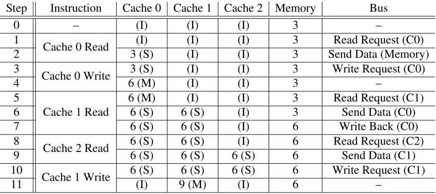
To further explain the MSI coherence protocol, Table 2.1 shows the contents of three
processed. The next three are for the contents of each of the caches. Their values are shown
as well as the current state shown in parentheses. The next column shows the contents of
main memory. Finally, the last column shows the current request that is on the bus along
[image:21.612.108.547.194.390.2]with the module that initiated in parentheses.
Table 2.1: MSI Cache Coherence Example
Step Instruction Cache 0 Cache 1 Cache 2 Memory Bus
0 – (I) (I) (I) 3 –
1
Cache 0 Read (I) (I) (I) 3 Read Request (C0)
2 3 (S) (I) (I) 3 Send Data (Memory)
3
Cache 0 Write 3 (S) (I) (I) 3 Write Request (C0)
4 6 (M) (I) (I) 3 –
5
Cache 1 Read
6 (M) (I) (I) 3 Read Request (C1)
6 6 (S) 6 (S) (I) 3 Send Data (C0)
7 6 (S) 6 (S) (I) 6 Write Back (C0)
8
Cache 2 Read 6 (S) 6 (S) (I) 6 Read Request (C2)
9 6 (S) 6 (S) 6 (S) 6 Send Data (C1)
10
Cache 1 Write 6 (S) 6 (S) 6 (S) 6 Write Request (C1)
11 (I) 9 (M) (I) 6 –
Step 0 shows the initial configuration of the memory; each cache is in theinvalidstate,
and the value in memory is 3. The first instruction is a read issued to cache 0. This takes two
steps to complete. The first is a read request sent by cache 0 to the other caches requesting
for a copy of the data. Since the other caches are in the invalid state, this request gets
ignored. Cache 0 gets a copy of the data from main memory in thesharedstate.
The next instruction is a write to cache 0 because the processor modified the data. Since
the copy in cache only has read permissions, a write request needs to be sent to the other
caches to invalidate their copies, if they have them. The other caches are already in the
invalid state, so the request is ignored. Once that is completed, cache 0 is free transition
into themodifiedstate as shown in step 4 when the value gets changed to 6.
The third instruction is a read issued for cache 1. To get a copy of the data, cache 1
issues a read request to the other caches before having to get it from memory. This time the
which downgrades the copy in cache 0 to thesharedstate since it no longer can have write permissions. By downgrading states, cache 0 also needs to write the data back to main
memory so it also has the updated copy. These three steps are shown as steps 5-7, and the
final result is caches 0 and 1 both have the updated copy in theshared state.
The next instruction is for cache 2, and it is also a read. The first step is to issue a read
request to other caches. Since both of the other caches have a copy that can be shared, it is
up to the cache manager to chose one to send the data. In this example, cache 1 sends its
data to cache 2. All three caches now have a copy of the data in thesharedstate.
The final instruction is a write to cache 1. To gain write permissions to be allowed to
modify the data, a write request is sent to the other caches. Since both caches have a valid
copy of the data, they both acknowledge the request. Both caches invalidate their copies
and when this is done, cache 1 is allowed to modify the data. The final result is that cache
1 has the only valid copy of the data in the modified state, which will eventually need to
be written back to memory. These five instructions needed 11 steps due to all of the traffic
that was needed to maintain coherence of data across all caches.
One optimization for this protocol is to add an additional state to reduce some unneeded
coherence traffic. Consider the scenario when a block of data is loaded into cache for
the first time. After the processor reads the value and wants to store a new value, an
invalidation request must be sent to the other caches in the same level. However, since this
copy is known to be the only copy that exists in cache, the invalidation request just added
unnecessary coherence traffic. A solution to this is to add a new state, exclusive, that is
similar to thesharedstate but is guaranteed to be the only copy in cache. Since it’s the only copy, it can already have write permissions so that when a store instruction transitions it to
themodifiedstate, there is no need to send out an invalidation request. The only caveat is when a another cache line requests the same data, the exclusivity is lost and this cache line
must be downgraded to thesharedstate. With the addition of the new state, the protocol is
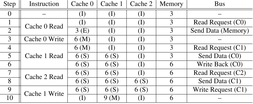
The same example is shown in Table 2.2 but this time using the MESI protocol. The
difference occurs when cache 0 reads the value for the first time and then modifies it. In
the MSI example, the value was read into cache 0 in theshared state even though it was
the sole copy. In the MESI example, this same value is read into theexclusivestate. Then,
when cache 0 is going to modify the data in step 3, it can do this without issuing any other
requests. The addition of this state removes the need for the unnecessary write requests
when only one copy of data exists across all caches. The remainder of the example is the
[image:23.612.108.547.291.472.2]same as the MSI since theexclusivestate has no impact on the other instructions.
Table 2.2: MESI Cache Coherence Example
Step Instruction Cache 0 Cache 1 Cache 2 Memory Bus
0 – (I) (I) (I) 3 –
1
Cache 0 Read (I) (I) (I) 3 Read Request (C0)
2 3 (E) (I) (I) 3 Send Data (Memory)
3 Cache 0 Write 6 (M) (I) (I) 3 –
4
Cache 1 Read
6 (M) (I) (I) 3 Read Request (C1)
5 6 (S) 6 (S) (I) 3 Send Data (C0)
6 6 (S) 6 (S) (I) 6 Write Back (C0)
7
Cache 2 Read 6 (S) 6 (S) (I) 6 Read Request (C2)
8 6 (S) 6 (S) 6 (S) 6 Send Data (C1)
9
Cache 1 Write 6 (S) 6 (S) 6 (S) 6 Write Request (C1)
10 (I) 9 (M) (I) 6 –
Accessing main memory is a huge delay, whether it be reading from or writing to it.
With either the MSI or MESI protocol, whenever amodifiedstate gets evicted, or replaced,
a write back to main memory is necessary because themodifiedstate had an updated value.
To avoid this, another state calledownedis added to the protocol. This state is also similar toshared state, but has the sole responsibility of writing data back to memory. There can be a scenario where all caches share an updated value but main memory still has the old
value. There needs to be one cache with the data in the owned state so there is only one
responsible of updating memory when it gets evicted. Another slight optimization is that
if the owned state gets evicted, rather than writing back the data, one of the othershared
protocol with theownedstate is called MOSI. The exclusiveandownedstates can coexist to form the MOESI protocol. This is a very powerful and well-known cache coherence
protocol for multiprocessor systems.
The coherence protocol commonly used in GPUs can be represented by an extension
of MOESI. Due to the extremely high level of parallelism in GPU applications, many of
the writes to the first level cache don’t conflict with caches in other SMs. Since there
are numerous writes that occur between all of the SMs in a GPU, the coherence traffic
needed to keep all L1 cache coherent is unnecessary. By extending the MOESI protocol to
allow GPUs to have some non-coherence in their L1 caches [15], the coherence bus is not
saturated with unneeded traffic. The extended protocol is known as NMOESI which adds
thenon-coherentstate for the first layer of cache [2].
Table 2.3 gives a brief description of six states in the NMOESI protocol. The first state,
non-coherent, is the state added for the L1 cache of GPUs. This state allows different L1 caches to simultaneously modify the same block of data locally. The changes are not
propagated to the other caches, so the changes in one L1 cache are not known to any other
cache. The obvious issue with this comes when multiple SMs modify the same block of
data. This process is handled when the block eventually gets written back to L2 cache.
Only the data that was modified within the block gets merged with the copy in L2. The
merging process is handled by a byte-mask where each bit in the mask represents each byte
in the block. The value of the bit determines if the byte has been modified and requires
merging [2]. This works since threads of different blocks don’t usually modify the same
bytes of data. In the cases that they do, atomic functions are used which don’t use this
non-coherentstate and force coherency between all caches.
The second state is themodifiedstate. This state signifies that changes have been made
to the block and all of the other copies in the same level of cache are invalid. While there
is a cache line in themodifiedstate, the values in lower level memory, (i.e. closer to main
Table 2.3:State Definitions for NMOESI Protocol
Letter State Description
N Non-coherent Locally modified copy that other caches don’t know about
M Modified Only valid copy and has been updated
O Owned One of several copies but has write back responsibility
E Exclusive Only valid copy of data, and it is unchanged
S Shared One of several copies and only as read permissions
I Invalid Invalid cache line, need to request data to be valid
rather than main memory so it is up to date.
Ownedis the third state of the protocol. This state exists when there are multiple copies of the block across the same level of cache, but this copy owns the right to write back its
data. This state allows for “dirty sharing” of the data. In the scenario when a line has
modified data and another cache requests the data, instead of writing the modified data to
memory, it drops from themodifiedstate to theownedstate and shares its data to the cache
that requested it. This means caches can share data that main memory doesn’t have an
updated copy of, which reduces unnecessary accesses to main memory. The value finally
gets written to main memory once theownedstate gets evicted.
The exclusivestate is the fourth possible state. This state signifies that this cache line has the only valid copy of the block in this level of cache. This state eases the transition
to the modified state by not needing to send an invalidation request to other caches since
this is guaranteed to be the only copy. If another cache in the the same level requests this
block, the exclusivity is lost, and the cache that had theexclusivestate must be changed to
theshared state.
The fifthstateis shared. When several copies exist across the same level of cache, they
are in thesharedstate. If the data has been updated, one of the caches has a cache line in
theownedstate. The difference betweenownedandsharedis that thesharedstate has no responsibilities to write back its data when it is evicted. It serves as a hit only when the
cache needs to read the data.
correct. Theinvalidstate is just the opposite, the data is not correct and cannot be used. It must be overwritten and changed into one of the valid states before this cache line can have
correct data.
Traditionally, all loads to cache are non-exclusive whereas stores are exclusive. Because
of this, the exclusive stores are forced to be coherent which requires a lot more coherence
traffic than the non-exclusive load accesses. The non-coherent store is a non-exclusive
store meaning the access requires less coherence traffic, similar to that of a load access.
This state allows for stores to the L1 cache of each SM without the overhead of keeping
coherency. This allows for multiple SMs to simultaneously modify the same block in their
own respective L1 caches. The blocks are then merged together with the byte-mask when
written back to the lower level of cache. The merging of the data is considered safe because
threads shouldn’t be modifying the same bytes of data in a block. When they do, atomic
functions should be used. The ability to have non-coherence applies to only the first level
of cache. The lower levels do not use thenon-coherentstate which means they follow the
MOESI protocol. This requires no change since it is a subset of NMOESI.
In today’s GPU systems, a store instruction is assumed to be anon-coherent storeto L1
cache. This is due to the vast number of store instructions that don’t need to be coherent
across all SMs of a GPU. However, there are some cases where writing data needs to be
coherent, so this is handled explicitly throughatomic storeinstructions. This means there
are three types of memory accesses handled by the processor in GPUs:loads,atomic stores,
andnon-coherent stores.
Table 2.4 gives a brief description of the possible actions that can cause a state transition
in the NMOESI protocol. The first three are processor actions. These are initiated by
executing a certain instruction. The load is any instruction that reads from memory. The
atomic store is an atomic write to memory. The SM that issues theatomic store needs to ensure that no other SM has its own locally modified copy. The final processor action is the
explicitly being atomic.
The next set of three actions are internal requests. The first is eviction. When a miss
occurs in a cache, one cache line needs to be overwritten by the newly requested data. This
is the action used to ready the line for overwriting, (i.e. invalidate and write back the data
if needed). The read request is issued when a new cache line loads in data. This is to notify
other caches that another copy exists in cache and to request the data so a memory access
isn’t needed. The write request is to notify other caches that a change is being made to one
copy of the cache line. This essentially means that all other copies should send their data
and be invalidated.
The final two are internal actions. These are responses to internal requests. The send
data response occurs when a cache gets a read or write request. The requesting cache needs
a copy of the data so this cache replies with its copy avoiding an access to main memory.
Write back occurs when a block needs to be evicted to make room for a new block. The
block that is getting evicted needs to store its data back to the next lower level of memory.
Table 2.4:Transition Actions in the NMOESI Protocol
Action Description
Load Processor executes a read from memory
Store Processor executes an atomic write to memory
N-Store Processor executes a write to memory
Eviction Internal request to overwrite the cache line
Read Request Internal request to notify other caches that another copy is going to exist
Write Request Internal request to notify other caches that their copy is no longer valid
Send Data Internal action to send a copy of the data to the cache that requested it
Write Back Internal action to write data back to the next lower level of memory
Table 2.5 shows the transitions between states that occur due to the transition actions.
The first column is the current state of the cache line. The next set of three columns gives
the actions issued by the processor while the final set of three columns shows the internal
actions to keep coherency. When the processor issues aloadand the cache line
correspond-ing to that address is in a valid state, then it registers as a hit and no other action is required.
Another cache in the same level may respond to the read request with the data so an access
to memory isn’t needed. If this occurs, the cache line transitions into the shared state. If
a memory access is required or a lower level cache responds, the line transitions into the
exclusivestate once it receives its data. Thestoreinstruction always transitions the line to themodifiedstate, if it wasn’t already. A hit is registered if the state was already modified or had exclusive rights to modify it. Every other state must issue a write request to other
caches in the same level to invalidate their copies before this cache can transition to the
modifiedstate. Anon-coherent storeis a little different. If the state already has write back responsibilities, (i.e.non-coherent, modified, or owned), then no other action is required. The other valid states must transition to thenon-coherentstate. An invalid line issues a read
request to downgrade other caches’ copies before transitioning to thenon-coherentstate.
When a cache line gets an eviction request, it means it must invalidate itself, if it’s not
already. Thenon-coherent,modified, andownedstates all have the responsibility of writing back their data which means they must send their data to the lower level of memory. After
they finish, then they can invalidate and be overwritten. Read requests are recognized only
by states that have ownership of their data. The non-coherent, shared, and invalid states
ignore these requests. Theownedstate responds by sending its data to the requester. The
modified and exclusive state also do this but they must be downgraded to the owned and
shared states, respectively, since they no longer have the sole copies of that data. Finally,
a write request makes all valid copies invalid. All valid states except for shared respond
with a copy of their data in case the requester is in the invalid state. With the write allocate
policy, a write miss requires the data to be loaded into cache before overwriting it with the
modified data.
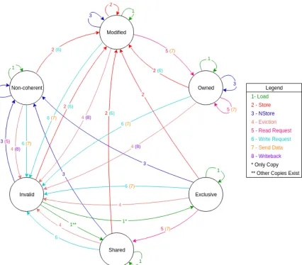
These transitions are visualized in a state transition diagram in Figure 2.3. The
transi-tions are color coded and labeled for a cleaner look. The action that caused the transition is
the first label, and the optional number in parentheses is a resulting internal action caused
Table 2.5:State Transitions for NMOESI Protocol [2]
Processor Actions Internal Actions
Load Store N-Store Eviction Read Req. Write Req.
Write Req. Write Back Send Data
N hit
→M hit →I – →I
Write Back Send Data Send Data
M hit hit hit
→I →O →I
Write Req. Write Back Send Data
O hit
→M hit →I Send Data →I
hit hit Send Data Send Data
E hit
→M →N →I →S →I
Write Req. hit
S hit
→M →N →I – →I
Read Req. Write Req. Read Req.
I
→S or→E →M →N – – –
is processed. These are differentiated by a single asterisk (*) or two asterisks (**). The
number of copies in the same level of cache dictates whether the state transitions toowned
orexclusive.
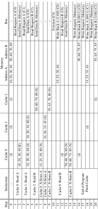
To further the understanding of the NMOESI protocol, Table 2.6 shows the cache
be-haviors when running a basic kernel. The function of the kernel is to add 5 to each byte
of a vector. The example uses an 8-byte vector initialized with multiples 10. The kernel is
designed to use 4 blocks, each with two threads. This means the first block handles the first
two bytes while the last block handles the last two bytes. In this example there are three
SMs which means only three blocks can be executed at a time, and the final block needs to
wait for a free SM. The caches can hold one block of data, which is 4 bytes. Even though
the thread block needs to access only two bytes of data, it must read data block of 4 bytes.
Table 2.6 is structured similarly to the tables of the previous cache coherence examples.
The differences this time are that each cache can hold a block of 4 bytes of data. Also, there
are two columns for main memory to hold the two blocks of data since the vector has a
length of 8 bytes. The addresses for these two blocks are A and B, respectively. Finally, the
table shows only when a change occurs. Blank cells have the same value as the cells above
structured in the follow way: each cache reads in the data for its thread block and modifies
it non-coherently. Then, one cache needs to repeat the process for the fourth and final
thread block. After that completes, the caches need to flush their modified contents to main
memory so the program can complete its execution.
Step 0 shows the initialization of the program. All of the caches start in theinvalidstate and memory has the 8 bytes of the vector across two addresses. The first instruction is for
cache 0 to read address A to get the first two bytes of the vector. Its first step is to issue
a read request to the other caches, but since the other caches are in the invalid state, the
request is ignored. Cache 0 must then wait for memory to send a copy of the data. Once
the block of data is received, in step 2, the cache line in in theexclusivestate since no other cache has a copy.
The second instruction is also a read to address A but for cache 1. The same address is
used since this cache is handling the second thread block which uses the third and fourth
bytes of the vector which is address A. A read request is issued again, but this time, cache
0 can acknowledge the request since it has a valid copy of the data. Cache 0 replies to the
request by sending its copy of the data as well as transitioning its copy from theexclusive
state to thesharedstate since its no longer the sole copy.
Cache 2 is executing the third thread block which means it needs to read address B for
its data. A read request is issued to the other caches, but neither of them have a copy of
address B so the request is ignored. Once the copy of data is received from memory, it is
put into cache in theexclusivestate. After these 6 steps, each cache has the data needed to
execute the first three thread blocks.
Steps 7-9 are the writes to cache for the first three thread blocks. These writes transition
the cache lines into thenon-coherentstates so there is no traffic on the coherence bus. This is safe to do because each thread block is accessing different bytes of data. After these three
writes are complete, the execution of the first three thread blocks are also complete. This
In this example, the final thread block is assigned to cache 0. To start the execution, the
cache needs to read in the bytes from address B, but the cache already has modified data
loaded. This needs to be evicted before the data can be overwritten. Step 10 is the eviction
request to cache 0 which cache 0 responds to by writing back its data to memory. However,
since the data was in the non-coherent state, the write back is slightly different. Along
with the data is a byte mask, shown in the square brackets. This example uses 1100 which
indicated that only the first two byte have been modified, thus only those bytes should be
written back to memory. This is what makes simultaneous modification of the same block
of data possible. After the write back has finished, the cache line can safely be invalidated.
Now the cache can issue a read request for the block of data at address B. While cache
2 does have a copy of address B, it is in the non-coherent state so it ignores the request.
Cache 0 must wait for memory to send the data. Once it has been received, it is put into the
sharedstate since cache 2 also has a copy, so it isn’t exclusive.
Step 14 is the final write to finish the execution of the final thread block. At this point
all of the thread blocks have finished execution. However, only one block has written its
modified data to memory; the rest still exist in a cache. At the end of the program, all of
the caches need to be flushed. This is a two step process for each cache. The first is a write
request sent to the cache. The cache responds to this by writing its data back to memory. In
step 16, cache 0 writes its data back with a byte mask of 0011 indicating that only the last
two bytes should be written. After this, the cache can invalidate its copy. This process is
repeated for each cache. Since the other two caches also have their data in thenon-coherent
state, they also write back data with a byte mask. The effects of this are easily shown in
steps 18 and 20 when looking at the contents of memory. Only the two bytes specified by
the byte mask are updated. At the end of this example, all of the caches have been flushed
2.3
Related Work
The work by Nimkar [4] paved the way for this research. His work explored the cache
access patterns of a GPU. By running various benchmarks on both NVIDIA and AMD
architectures, he was able to compare cache hit ratios, most and least recently used cache
lines, as well as inter- and intra-warp localities. Both architectures showed lower hit ratios
than those of a CPU due to the way GPUs maintain performance compared to a CPU.
GPUs balance memory misses by having a multitude of threads ready to execute whereas
the CPU has a small number of threads but a much bigger cache to minimize cache misses.
Nimkar conducted his research by simulating both GPU architectures with Multi2Sim. By
modifying the source code, additional metrics were recorded. To measure the inter- and
intra-warp locality, several counters were added to the simulator, and the counts were added
to the simulation reports after running a benchmark.
The idea of modifying the cache architecture of a GPU has been proposed before.
Samavatian et al. [16] propose a new type of L2 cache in order to combat the high power
usage of the conventional L2 cache. To test their proposed design, a cycle accurate GPU
simulator, GPGPU-Sim was used. Samavatian et al. observed that as conventional SRAM
technology gets smaller, the amount of leakage current increases tenfold. This meant newer
architectures used smaller cache technologies that leaked more current and thus consumed
more power. They proposed switching the L2 cache to a spin torque transfer RAM
(STT-RAM). This type of RAM is high density while having low leakage power. The downside
to it that is has high write latency and energy. To mitigate these drawbacks, the L2 cache
was split into a low retention and high retention section. The low retention section holds
data that gets rewritten at a high frequency since it takes less energy to write to but doesn’t
retain very long. The other section takes more energy to write to it but can retain data for
much longer. The findings with this new L2 cache architecture were that the power was
on the chip was reduced significantly since the new STT-RAM architecture is four times as
dense as conventional SRAM.
Another possible modification to the cache architecture is modifying the cache
coher-ence protocol. Candel et al. [17] used another cycle accurate GPU simulator to implement
a simpler cache coherence protocol. They wanted to accurately model the memory system
for GPUs for both on- and off-chip memory. To simulate the work and on-chip memory of
the GPU, they used the cycle accurate simulator Multi2Sim. Another simulator,
DRAM-Sim2, was used in conjunction with Multi2Sim to simulate the off-chip memory. The target
GPU they wanted to model was an AMD Southern-Islands 7870HD. This card uses a
sim-pler cache coherence protocol than what Multi2Sim uses, so they had to modify the source
code to add this capability. The new protocol adds two bits to the instructions to determine
where to access memory. The two bits are system level coherent (SLC) and global level
coherent (GLC). The SLC bit indicates memory accesses should bypass cache completely
and access main memory. The GLC bit is dependent and reading or writing. When reading,
it means to bypass L1 and search L2. When writing, the data gets written to L1, and the
GLC bit determines if the evicted line gets written back to L2. Another contrast from the
NMOESI protocol is that the L1 caches use a write through policy. The L2 cache still uses
write back, however. The conclusions from this paper were that the modified simulator
more accurately models the AMD Southern-Islands 7870HD GPU than the original
simu-lator. They determined this by running various performance metrics in the simulator and
on the actual GPU.
Ziabari et al. [2] show that the NMOESI protocol can be used in more than just a GPU.
Their work proposes a novel hardware-based unified memory hierarchy to ease memory
management between a CPU and one or more GPUs. The reasoning behind using NMOESI
to connect a CPU with a GPU is because the common multi-core protocol, MOESI, is a
subset of NMOESI. This means all of the operations needed to keep coherency across
support it. By evaluating the design, the results showed a performance improvement of
92%, and it also improved the CPU’s access to GPU’s modified data by at least 13 times.
In addition to all of this, performance also increased as the number of GPUs increased,
proving to be a very scalable design.
Koo et al. [6] have shown that the locality of the data has significant impact on cache
performance. The proposed work is a new cache manager which dynamically changes its
behavior based on the locality of load instructions. Again, the work was evaluated using a
simulator, GPGPU-Sim. Koo et al. observed that threads have one of four types of locality:
streaming data, inter-warp locality, intra-warp locality, or a mix of both warp localities.
Streaming data is data that is accessed only once. Inter-warp and intra-warp localities are
when bytes of data are shared between threads from multiple warps and threads within the
same warp, respectively. In addition to this, all threads in a warp share the same type of
locality. A single warp is monitored to determine the type of locality and then based on
this, the proposed cache manager protects the cache line fetched by the load or completely
bypasses cache. To evaluate their proposed design, a wide variety of benchmarks were used
across several different GPU architectures. The benchmarks varied their reliance on cache
from highly sensitive to highly insensitive. The architectures included both NVIDIA’s
Ke-pler and Fermi architectures. The results from the evaluation were that the cache sensitive
applications had an increase of up to 34% while the average of all was up 22%. They also
report a savings of 27% in power consumption.
While GPUs have gained popularity in general purpose computing, machine learning
has greatly improved by its massively parallel capabilities. Since the GPU is still designed
for the general purpose, a new coprocessor called a tensor processing unit (TPU) was
de-signed especially for machine learning. The TPU is a custom made ASIC by Google for the
inference phase of neural networks. This is the prediction phase after the network has been
trained. The idea behind designing this coprocessor was to remove anything unneeded
necessary. The architecture of the TPU is defined in [18]. There is a matrix multiply unit
that takes a variable sized inputBx256. It uses a constant weights of 256x256 to multiply
to get the variable output in B cycles. There is an activation pipeline that can apply the
activation function, such as ReLU or Sigmoid. Also, there is dedicated hardware that can
perform pooling operations. The memory hierarchy is composed of 28 MB of software
managed on-chip memory and surprisingly, no cache. The idea for not having a cache is
the hardware is specialized towards one specific machine learning application so there is
no need for cache.
Another type of processor that can be used for machine learning is called a
field-programmable gate array (FPGA). A benefit to using an FPGA is hardware acceleration.
By implementing a design in hardware, it is specifically made for that application.
Hard-ware typically runs faster than softHard-ware, and there is also the added benefit of lower power
consumption in hardware. Xilinx has their own deep neural network engine called xDNN
[19]. These FPGA implementations outperform GPUs by having lower latency with a
smaller batch sizes during the inference phase. This is because a GPU needs a large batch
size since it relies on massively parallel applications. By not having to wait multiple
in-puts, computation can occur as soon as the first input is ready, thus reducing latency. The
FPGA implementation also has the advantage of having consistent throughput throughout
the entire application. GPUs have a much higher throughput but are limited by the CPU
which has a much lower throughput.
Wang et al. [20] also used an FPGA because of the hardware benefits. Their work
im-plements a deep learning accelerator unit on an FPGA. They noticed as neural networks are
exploding in size, the power consumption by data centers is also increasing at an alarming
rate. While GPUs can still outperform an FPGA, the power consumption of an FPGA is
much less than that of a GPU while still getting moderate performance. The FPGA design
is also scalable making different network topologies possible. Analysis of their
Methodology
This work was conducted using a cycle accurate GPU simulator called Multi2Sim. This
simulator features the ability to configure the architectures that it is simulating to allow
for newer architectures to be emulated. The simulations were of benchmarks from two
suites. One of the suites consisted of benchmarks for general purpose algorithms that are
generally run on a GPU. The second is a suite of common machine learning algorithms
that also benefit from being executed on a GPU. Section 3.1 goes into more detail about the
simulator and how it was used. Section 3.2 explains the benchmarks used in this research.
3.1
Multi2Sim
There are two ways to explore the cache on a GPU: use a variety of GPU cards with varying
cache sizes and run different analysis benchmarks on them, or use a simulator that allows
for GPU architecture configuration and run those same benchmarks. The former would
yield real world results at the expense of owning multiple different cards. The latter is
much more feasible in terms of requiring less actual hardware and can still produce results
comparable to the performance from a real GPU.
The simulator that was chosen to perform this research was Multi2Sim [21]. It was
chosen over other simulator programs for a few of reasons. Among them was the ease of
in-stallation and modification as it was open source, well documented, and widely supported.
and provided the most accurate functionality for many different GPU architectures [4]. The
most recent version, 5.0, was used for this research. AMD’s Radeon Southern Islands and
NVIDIA’s Kepler architectures are the supported GPU architectures that can be emulated;
however, only NVIDIA’s Kepler series was targeted.
The architecture configuration and memory hierarchy were both fully configurable and
could be modified for each simulation. This allowed for many different configurations to
be run with relative ease. Getting results from the simulations was just as simple. On its
own, Multi2Sim came with the ability to report various statistics based on how detailed of
a simulation was run. These reports showed the configuration of the architecture used in
the simulation and statistics about it such as core utilization among others. In addition to
the architecture report, a memory report could also be generated with a detailed simulation.
This report summarized the memory hierarchy as well as included cache hit and miss ratios
[21]. Since Multi2Sim is open source, additional statistics could be recorded and displayed
in the reports with some simple changes to the code. Nimkar [4] has done this in his work
to report statistics on intra- and inter-warp hits as well as counters for the most recently
used sets of the cache.
3.1.1 Kepler Architecture
Multi2Sim can model the architecture based on NVIDIA’s Kepler series. The structure of
the architecture is configurable, from the number of SMs, all the way down to the routing
of data between specific nodes in the interconnects. To get realistic results, the architecture
must be configured to mimic a real Kepler series GPU. The default memory hierarchy that
Multi2Sim uses is close to the actual architecture, but there needs to be some modification
in the size of the L2 cache. The default characteristics of both cache modules and the main
memory module are shown in Table 3.1. It should be noted that even though the simulator
uses the name Kepler for the architecture, the ability to configure the architecture allows
Table 3.1:Default Module Characteristics for Kepler’s Memory Hierarchy
L1 Cache L2 Cache Main Memory
Latency (Cycles) 6 20 300
Replacement Policy LRU LRU –
Block Size (B) 128 128 128
Associativity 4 way 16 way –
# of Sets 32 32 –
Module Size (KB) 16 64 –
Table 3.2 shows a comparison of some of the characteristics between the different
gen-erations of NVIDIA architectures. The number of SMs increases with the newer
architec-tures after Kepler. Another difference between them all is the number of CUDA cores per
SM. Kepler has the most at 192, but newer generations drop. This is because there is less
overhead with fewer cores and newer technology still allowed for an increase in
perfor-mance. The cache sizes have also varied with the generations. Fermi, Kepler, and Volta
all have a combined L1 and shared memory. This allows for some configurability of how
much to use per program. Fermi and Kepler have a total size of 64 KB while Volta has
twice that at 128 KB. Maxwell and Pascal both have a dedicated 24 KB L1. Maxwell has
96 KB of shared memory while Pascal dropped this to 64 KB. Finally, the L2 cache size
is an ever increasing trend. Fermi started with 768 KB, but each generation increased all
the way to 6 MB with Volta. One conclusion that can be made from this table is that the
cache, L2 in particular, is consuming large amounts of hardware in each new generation.
Although this work focuses on the Kepler architecture, the findings and conclusions will be
applicable to newer architectures. One characteristic not mentioned in the table is the
as-sociativity of the caches. While it is known that the caches use a set-associative placement
policy, the number of sets and associativity are not disclosed. The only way to find this out
is to benchmark the caches [10].
All of the values mentioned in Table 3.1 can be modified via a configuration file. Some
of the options, such as the replacement policy, do not apply to main memory modules so
Table 3.2: Comparison of Various NVIDIA Architectures
Fermi [22] Kepler [8] Maxwell [23] Pascal [11] Volta [9]
# of SMs 16 14 24 56 80
CUDA Cores/SM 32 192 128 64 64
L1 Cache Size (KB) 16 / 48 16 / 32 / 48 24 24 up to 96
L2 Cache Size 768 KB 1536 KB 2 MB 4 MB 6 MB
Shared Memory
48 / 16 48 / 32 / 16 96 64 up to 96
Size (KB)
it is calculated by multiplying the number of sets, block size, and associativity together.
This is the size of each cache module which is how the L1 cache size is usually specified.
Since the L2 cache is shared between all SMs, its actual size needs to take into account the
number of modules and multiply that by the module size.
Figure 3.1:Block Diagram of the Memory Hierarchy of NVIDIA’s Kepler Architecture
The structure of the hierarchy is shown in Figure 3.1. There are 14 SMs, each with their
own local L1 caches. There is one network interconnect that connects each of the 14 L1
L2 cache to its own main memory module. Each main memory module serves a specific set
of addresses in global memory. The two types of ways to define an address space are with
an address range or by address interleaving. The simpler of these two is the address range.
There is a lower and upper bound, and if an address falls between the two, that memory
module serves that address. With address interleaving, the modulo operator is used on the
address and the result determines which module serves it. For example, with six modules,
the address would bemod6 and the first module would serve all addresses that result with 0
while the last module would serve results of 5. Interleaving has a little harder calculation to
do, but it splits up work much better, especially when dealing with consecutive addresses.
A separate configuration file can further modify the interconnects between each of the
modules. The configuration goes as far as allowing manual routing of data between
dif-ferent nodes and switches. This work uses the default for the GPU configurations of just
specifying the networks and using the Floyd-Warshall algorithm for routing [21]. There
are a total of seven networks: one connecting all L1 modules to all L2 modules and six
between each L2 module and a main memory module. All networks have three variables
that are specified. The first is the default bandwidth. The configuration file specifies 264
bytes per cycle for all networks. The other two variables are the input and output buffer
sizes. These are specified in number of packets and set to 528 each.
3.1.2 Limitations and Modifications
Since Multi2Sim is an actively developed open source project, there are bound to be
lim-itations in the simulations. To simulate the CUDA framework, the functions needed to
be redefined in the simulator source code. This is necessary because the functions need
to work with the software defined GPU rather than looking for an actual GPU connected
to the computer. Because of this, however, not all of the CUDA API function calls are
implemented which limits the programs that can be simulated. For example, the function
version of CUDA. This function is used by the CPU to initialize the constant memory of
the GPU for use in the execution of a kernel. Since this function is needed to use constant
memory, any program that uses it will not be able to be simulated using Multi2Sim.
Another limitation of the simulator is unrecognized instructions. The programs can
be compiled, but when they are run and there is an instruction that wasn’t implemented
by Multi2Sim, a segmentation fault occurs. The error message says there was an
unrec-ognized instruction at some program counter value. To determine which instruction is at
that value, the CUDA binaries, called cubins, need to be debugged. The cubin file can be
created using thenvcccompiler with the flag--cubin. After this, the assembly for the
device code needs to be dumped. This is done using programcuobjdump with the flag
-sass. For example, using the exponentiation functionexpf()produces the assembly
instructionFMUL32I. This is a single precision floating point multiply instruction which
is not supported. This is just one example of an unsupported instruction. There are more
such as other floating point computations as well as type conversions that are unrecognized
instructions.
There are a couple of ways to get around these limitations. The most obvious way is
to implement the unsupported features as the simulator is open source. This would take
a lot of additional time developing and testing the implementations. Another workaround
would be to use different functions that may degrade the performance if accurate
calcula-tions are needed. However, since this research is focusing on memory usage and not so
much on precision or accuracy results, another workaround was used. For example, instead
of implementing the complicated calculation, such asexpf(), a simple multiplication can
be done instead. This of course is going to give incorrect results, but since the result has
no effect on which memory addresses are used there will be no impact on cache
perfor-mance. The ALU still takes in the same parameters, and a result is produced. The incorrect
calculation acts the same from the viewpoint of the cache.
![Table 2.5: State Transitions for NMOESI Protocol [2]](https://thumb-us.123doks.com/thumbv2/123dok_us/62679.5874/29.612.118.536.92.306/table-state-transitions-for-nmoesi-protocol.webp)