SUPER SIX
S-1
.
00 Single
Board
Computer
-
Technical
-
Manual
«j>
ADVANCED
DIGITAL
USA OFFICE
5432 PRODUCTION DRIVE HUNTINGTON BEACH, CA 92649
TELEPHONE : (714) 891-4004
CORPORATION
UNITED KINGDOM OFFICE
27 PRINCESSS STREET HANOVER SQUARE, LONDON W1 R8NQ
UNITED KINGDOM 409-0077 / 409-3351
SUPER SIX™
S-lOO Single Board Computer
Technical Manual
TABLE. OF CONTENTS
SECTION
TITLE
SECTION I - JNTRODUCTION
1.1
Purpose
1.2
Equipment Overvie'W
1.3
Document Organization
1.4
List of Acronyms
1.5
Document Maintenance
1.6
Theory of Operation
SECTION II - OPERATION
2.1
2.2
2.3
2.4
2.5
2.6
2.7
2.8
2.9
2.10
2.11
2.12
2.13
2.14
2.15
2.9.1
2.9.2
2.9.3
2.9.4
Floppy Disk Controller
128K Dynamic RAM
System Monitor EPl{OM
Serial Ports
Para1Jel Ports
Real Time Interrupt Clock
S- 100 Bus Interface
Baud Rate Jumper
EPROM and Monitor Operations
EPR OM Enable and Disable
Monitor Sign-on
Monitor Commands
Cold Start Program
RAM Organization
Z80A DMA Features
PSNET /1 Operation
PSNET /PAR Operation
Synchronous Operations
Power Consumption
SECTION HI -INPUT/OUTPUT POR TS
3.1
Input/Output Port Assignments
3.2
Input/Output Descriptions
3.2.1
Port 00
3.2.2
Port 01
3.2.3
Port 02
3.2.4
Port 03
3.2.5
Port 04
3.2.6
Port 0.5
3.2.7
Port 06
3.2.8
Port 07
3.2.9
Port 08
3.2.10
Port 09
3.2.1 1
Port OA
3.2.12
Port
DB
3.2.13
Port OC
3.2.14
Port OD
3.2.15
Port
DE
3.2.16
Port OF
3.2.17
Ports 10-13
TABLE OF CONTENTS (continued)
SECTION
TITLE
PA~E3.2.18
Port 14
16
3.2.18.1
Port 14 Read Opera
tion
16
3.2.19
Port 15
17
3.2.19.1
Port 15 l{ead Operation
17
3.2.19.2
Port 15 Wri te Operation
17
3.2.20
Ports 16 and 17
17
3.2.20.1
Port 17
\\I
ri te Operation
18
3.2.20.2
Port 17 W rite Operation
l~3.2.21
Ports 18-1B
21
j
SECTION IV - JUMPER CONNECTIONS
22
4.1
Jumper Definitions
22
4.2
Jumper Descriptions
23
4.2.1
Jumper A
23
4.2.2
Jumper B
23
4.2.3
Jumper C
23
4.2.4
Jumper D
24
4.2.5
Jumper E
24
4.2.6
Jumper G
24
4.2.7
Jumpers Hand T
24
4.2.8
Jumper J6
24
4.2.9
Jumper R25
25
4.2.10
Jumper J7
25
4.2.11
Jumpers P, N, M, K, J, R, S, and F
2.5
4.3
Factory and OEM Installed Jumpers
26
4.3.1
8-lnch Floppy Disk Drive
26
4.3.2
~hugartSA800/801 Disk Drive
26
4.3.3
Shugart 850 Disk Ori ve
27
4.3.4
MFE Model 700 Disk Drive
27
4.3.5
Tandon Slim Line Disk Drive
27
4.3.6
N EC Model FD 1160 Disk Drive
28
4.3.7
QUME Data Track Disk Drive
28
4.3.8
Tandon 5.2.5 Inch Disk Drive
28
4.3.9
Mitsubishi Model 2894 Disk Drive
28
4.3.10
Mitsubishi Model 2896 Disk Drive
28
4.3.11
Shugart SA 860 Disk Drive
28
4.3.14
Siemens FDD-I00-8 Disk Drive
29
4.3.16
Qume Trak 592 5.25 Inch Disk lJrive
29
4.3.17
All Other Disk Drives
29
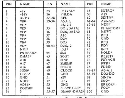
SECTION V - EXTERNAL CONNEC10R PINS
30
TABLE OF CONTENTS (continued)
SECTION
TITLE
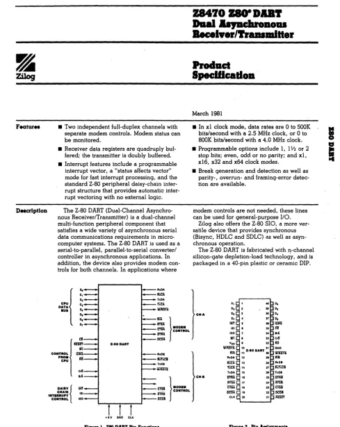
APPENDIX A - Z80A/Z80B SIO AND DART
APPEN DIX B - Z80A/Z80B PIO
APPENDIX C - Z80A/Z80B eTC
APPENDIX
D -
Z80A/Z80B CPU
APPENDIX E - 280 DMA
APPENDIX F - FLOPPY DISK CONTROLLER
APPENDIX G - FLOPPY DISK El{ROR CODES
APPENDIX H - APPLICATION NOTES
APPENDIX I - SUPER SIX WARRANTY
APPENDIX J -PARTS LAYOUT AND LIST
APPENDIX K - PLL REALIGNMENT
APPENDIX L - PSNET/l SCHEMATICS
APPENDIX M - PSN ET /PAR SCHEMA TICS
APPENDIX
N -
SUPER SIX SCHEMA TICS
FIGURE NO.
2-1
2-2
TABLE NO.
1-1
2-1
2-2
3-1
3-2
4-1
5-1
5-2
5-3
5-4
5-5
LIST OF FIGURES
TITLE
SUPER SIX Interface To the S-100 Bus
SUPER SIX RAM Configuration
LISl OF TABLES
TITLE
List Of Acronyms
SUPER SIX Baud Rate Jumper Settings
Monitor Commanas For the SUPER SIX
I/O Port Assignments For the SUPER SIX
SUPER SIX Port 18 Baud Rate Settings
SUPER SIX Jumpers and Abbreviated Functions
SUPER SIX J I Connector Pin Functions
SUPER SIX J2 Connector Pin Functions
SUPER SIX J3 Connector Pin Functions
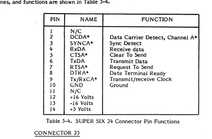
SUPER SIX J4 Connector Pin Functions
SUPER SIX J5 Connector Pin Functions
PAGE
6
11
PAGE
2
7
9
13
21
22
SECTION I
INTRODUCTION
1.1
PURPOSE
This Manual provides the technical information necessary to mstall, uperate dna maintair.
the SUPER SIX singleboard computer by Advanced Digital Corporation.
1.2
EQUIPMENT OVER VIEW
SUPER SIX, produced by Advanced Digital Corporation, is the first single board computer
for the S-IOO bus running at 6MHz. Without the S-100 bus the SUPER SIX can also run. as
a standalone computer executing a single user CP/M 2.2 or 3.0, or a multiuser MP /M,
OASIS, or TurboDOS operating system. SUPER SIX runs substantially faster than any
other S-l 00 single board computer a vialable in the market.
The SUPER SIX contains the following set of capabilities:
1.
280B CPU operating at 6MH2
2.
128K of dynamic bank se lect RAM arranged in 16k banks
3.
Floppy Disk Controller which supports the 8-inch and 5.25-inch disk
drives simultaniously
4.
2/4
K
of shadow EPROM (Monitor)
5.
2 serial I/O (RS-232) ports offering software or hardware selectable
baud rate, 280B DAR T
6.
2 parallel ports (280B PIO)
7.
Real time clock (280B CTC)
8.
DM A controller (280 DM A)
9.
Extended addressing: A 16-A23
10.
Single 5 volt supply on board
11.
One-year warranty
12.
Free copy of CP/M 2.2 BIOS supplied.
1.3 "
This document is organizt'd
inh' ')
sc\.·t
i,-'Ils ..
md
14
.lppcndices.
Section I serves as an introductioll to tht' entire document, stating the purpose of the
document and providing an introduction to the SuPER SIX single board computer. This
section also provides a list of acronyms used in the document and provides a statement on
the responsibilities of document maintenance.
Section II provides a description of the operations of aU components associated with the
SUPER SIX single board computer.
Section III lists aU SUPER SIX input/output ports and defines the assignments and
functions of each port.
Section IV lists and defines aJJ SUPER SIX jumper connections. This section includes the
jumper ,assignments for factory (OEM) installed jumpers.
Section V describes the external connector pins for SUPER SIX connectors
J
1 through
J
5.
The appendices provide supplemental material to the body of the text and are referenced
in the text at the associated points.
1.4
LIST OF ACRONYMS
Table 1 -1 provides a listing and description of the acronyms used within this text.
ACRONYM
DESCRIPTIO~CPU
Central Processor Unit
CTC
ControJJer /Timer Circui t
DART
Dual Asynchronous Receiver/Transmitter
DMA
Direct Memory Access
EPROM
ElectricaUy Erasable Programmable Read-Only Memory
FDe
Floppy Disk Controller
IEEE
Institute of Electrical and Electronic Engineers
MP/M
Multiuser Program For Microcomputers
OEM
Original Equipment Manufacturer
PIO
ParaUel Input/Output
PROM
Programmable Read-Only Menlory
Table
I-I.
List
of
Acronyms (Continued)
ACRONYM
DE~CRIPTIOi\1.5
RAM
Random Access Memory
SIO
Serial Input/Output
TTL
Transistor-transistor Logic
TurboDOS A Multiuser Networking Operating System used as software with the
SUPER SIX
DOCUMENT MAINTENANCE
This document is the property of Advanced Digital Corporation, who is responsible for its
content. Any modifications made to this manual must be made with the express written
approval of Advanced Digital Corporation.
1.6
THEOR Y OF OPERATION - ST ART-UP PROCEDURE
The SUPER SIX Single board computer is shipped configured for 19.
installation procedure is as follows:
baud rate. The
1.
Plug the PSNET /1 to connector J5. Use caution; pin 1 is marked.
2.
Connect the CRT. Pins 2, 3, 5, 7, and 20 must be used; no parity
must be specified,
3.
Apply power to the system.
The monitor message shown in
subsection 2.9.2 appears. Check the CRT baud rate-
if
9600 baud is
required, unplug jumper area J7, pin 7-8.
4.
Install the floppy disk cable, load the CP/M diskette, and bootstrap
the system.
Note: CP/M is shipped configured for 64K bytes of
memory. The parallel port is configured as the default
printer.
1024 bytes per sector read/writes are also'
SECTION II
OPERATION
This section describes the opera tion
01
all
SUPER SIX <;:ompone.nts.
2.1
FLOPPY DISK CONTROLLER
The floppy disk controiJer can access up to four 8-inch or four 5.25-inch disk drives or any
combination of the two. The controller can read and write ISIv1 3740 single density format
and double density 1024 sector-SIze formats. Data transfer
is
performed via Direct
Memory Access (DMA). Due to the simultanious operation capability of the SUPER SIX
the format compatibility problems with 5.25-inch disks have been eliminatea. The floppy
disk controller used is the
WD27~3.The WD2793 has on-chip PLL ,data separators and
on-chip write pre-compensation logic. Adjustments for PLL are factory set dnu write
pre-compensation has been provided with the SUPER SIX. 50 Pin and 34 pin connectors
are available for 8-inch and 5.25-inch disk drives respectively.
2.2
NOTE: Customer adjustment of trim pots
may result in cancellation of warranty.
THE 128K DYNAMIC RAM
The 128K RAM array can be switched ON and OFF in 16K increments, (0-16K, 16K-32K,
32K-48K, 48K-64K for both banks) under soitware control. This feature allows the CPU
to access bank switchable external memory on the S-IOO bus. The memury has an access
time of 150ns. A Refresh operation is performed during Z80 M I cycles and during
\V
AIT
and RESET states. The memory can be accessed by floppy dIsk via
D~iA,serial and
paralle 1 'I/O, or another DMA device un the S-l 00 bus.
*NOTE: Any external DlV1A device that is
using continous mode DMA cycles must
transfer data at an average rate of 1501s per
byte or faster when holding the DMA request
line for more than 1.5I11s.
The RAM row
address is the low order address; therefore
the entire RAM array is refreshed
by
DMA
device every 128 contiguous memory cycles.
Under CPM 2.2 or CPM 3.0 the additional 64K can be used as a dISk buffer. The ·SUPER
SIX is ideal when operating in the bank mode under CP/M 3.0, as 128K RAM is required.
2.3
SYSTEM
MONIT01<
EPHOM
The system monitor
t.PHOM
is switched
ON
during reset.
Jt C~II t)(~ (jj~~t.Jl(:a dr,G(:rlabled
under software control.
When enabled, the system IIluflltor r(:sjrj(:C)
dtlocations
F800-FFFF (hex) (refer to subsection 2.9.1.2)
whenusing
1716 Ll't<U,\'or
CItlocations
FOOO-FFFF (hex) when using the 2732
EPRL'M.
lhe
~>stelrrI/lonitur
LP~lIMcontains the
cold-start loader for
CP /tvl, MP
/1\1
and
1
urboDl.\).
In
.:idunia! I j t Cdn De used
to
perform
LOAD,
I/O
READ and
1/0
'W RITE operations. 'When the
LP1.(,-).vi
is disablea no system
address space is used.
2.4
SERIAL PUR IS
A 6MHz Z801:) DAR
T
is used for the two serial I/O ports; a 2:805
,)10
or Z80A DAH T can
be used in it's place
(ifa 4MHz Z80A DAR
T
is used the
CPU
and all other devices must
also be 4MHz). This allows asynchronous serial data communication plus a variety of
interrupt modes. Modem control signals are available at each serial connector. There are
software selectable baud rates as well as hardware selectable baud rates (mini-jumpers
J7).
2.5
*
NOTE: The serial ports are TTL and must
be connected to
PSN ET/
1
(serial adapter
interface) for RS-232 communications. The
J4 connector is for
the
CR T;
the J5
connector is for the serial printer or CH T.
PARALLEL POl{
15
A 6MHz 280B PIO is used as the parallel port. The "A" channel of
this
chip is used to
connect the parallel port connector (J2) to
PIO.
This port has an 8-bit bi-directional data
line and two hand-shake
lines.
1
he
"13"
port can be
split
between the parallel port
connector and the
5-100
bus vectored interrupts lines by jumper options. This allows the
port to be used as an additional paralJel port, an interrupt controller, or both of the
above. In the output mode the parallel ports can drive one TTL load.
2.6
REAL
TIME
INTERkUPT
LLOCK
A 6MHz 280B eTC is used for providing a real time system clock for
tvlP /M
or TurboDOS
operating systems. Three channels of the eTC are available to the user for jumpering to
synchronous baud rates or
long clock
times.
2.7
S-IOO
BUS
IN1ERFACE
The 5-100 bus interface provides the signals necessary for an 8-bit bus master as
described by the lEEE-696 bus specification.
Vectored interrupt lines VIO- V 17 are
supported via jumper options (refer to section I V) and A 16-A23 are
also
supported via an
1/0
port. The Phantom line is also implemented for the dynamic
RAM
array.
I
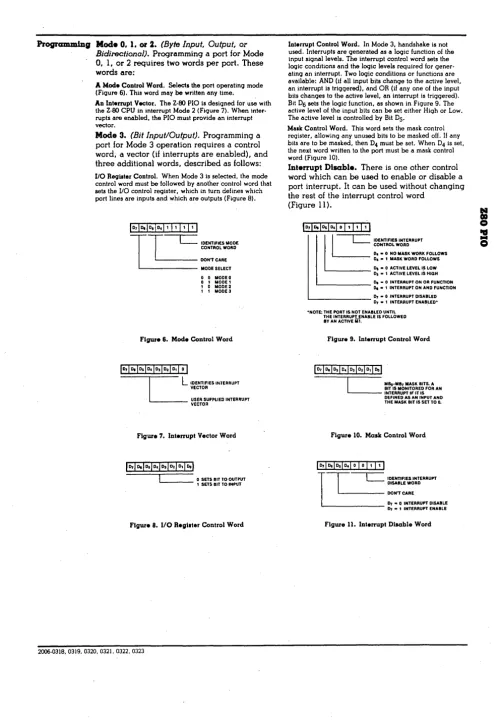
(j\
I
CONNECTOR
J2
P~RALLEL
PORTS
CLOCK
DATA
RECEIVERS/
DRIVERS
JUMPERS
DMA
EPROM
2K,4K
VI
LINES
5.:100
ADDRESS
DRIVERS
CONNECTOR
J3
CONNECTOR
J1
FLOPPY DISK
CONTROLLER
CPU
5-100
BUS
-CONNECTOR
J4
RAM ARRAY
64K
A
SERIAL PORTS
CONNECTOR
J5
B
2.8
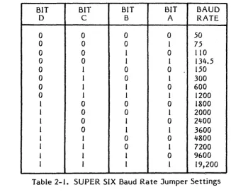
BAUD RATE JUMPER
Upon SUPER SIX initialization, the baud rate for the two serial channels can be
hardware-selected independently by means of the baud rate jumper (J7). This 7-pole
jumper is located between U70 and U68 and is divided into two sets of jumpers containing
four and three pins for 510 channels A and B, respectively. Pins 7, 6, 5, and 4 set the baud
rate for 510 channel A and are designated as A, 5, C, and D, respectively; pins 3, 2, and I
set the baud rate for 510 channel B and are designated as A, B, and C, respectively.
Because this jumper comprises of only seven pin sets, SIO channel B has a hardware
limitation of 1200 baud; by means of port 18 the software may be set to allow up to 19.2K
baud for channel B. The baud rate settings, as determined by this jumper, are shown in
Table 2-1, below. Once the SUPER SIX is initialized, I/O port 18 is used to modify the
baud rate. Port 18 is described in subsection 3.2.21.
BIT
BIT
BIT
BIT
BAUD
D
C
B
A
RATE
0
0
0
0
50
0
0
0
I
75
0
0
I
0
110
0
0
I
I
134.5
0
I
0
0
150
0
I
0
I
300
0
I
I
0
600
0
I
I
1
1200
I
0
0
0
1800
I
0
0
I
2000
1
0
I
0
2400
I
0
1
I
3600
1
1
0
0
4800
I
I
0
I
7200
I
I
I
0
9600
[image:12.618.127.453.205.477.2]I
I
I
I
19,200
Table 2-1. SUPER SIX Baud Rate Jumper Settings
2.9
EPROM AND MONITOR OPERATION
The on-board EPROM occupies addresses
FOOO-FFFF
(hex). This EPROM is switched ON
automatically during RESET or POWER-ON.
It
contains the serial input/output (510) and
floppy disk controller
(FDC)
initialization code along with a simple debugger and floppy
disk cold-start loader. After the operating system is loaded the EPROM can be turned
OFF
to allow access to the RAM at address
FOOOH-FFFFH.
The EPROM can be enabled
or disabled at any time to permit the calling of hardware dependant
lio
routines.
2.9.1
EPROM Enable/Disable
BAUD RATE JUMPERS
ADVANCED DIGITAL CORPORATION SUPER SIX SUPPLEMENT
Update for Page 7
With the Super Six component side facing you and the S-100 cunnector down there
are 7 jumpters between U68 and U70 aligned vertically.
There are assigned as
follows:
<I III
bit A
1111
bit B
JUMPER INSTALLED
1
1111
bit C
1111
bit D
JUMPER OFF = 0
console -SIO CR. A=
-SIO CR. B=
~III1
bit A
1111
bit B
1111
bit C
Bit D for SIO CR. B is not available as a jumper and must be set in software.
Bit 7 of this input port (port 15) is instead used to sense double sided drives.
Some software reads this bit and sends it to the SIO CR. B baud rate anyway. If
you have double sided drives, this will make the bit a 0 thru creating baud rates
from 50 to 1200.
If you have single sided drives, this will make the bit a
1
and create baud rates from 1800 to 19.2K.
If you experience a problem with this
you can make a file under cpm to correctly assign the baud rate to SIO CH. B
(used for serial printer and/or modem) as follows:
Console
SIO CR. B
(ON )
(ON )
(ON )
(ON )
(ON )
(off)
(ON )
19.2k
=
300
A)ddt
-a100
in 15
0100
0102
ani 7f (for 50 to 1200 baud. for 1800 to
19.2k type ori 80)
0104
0106
0109
-gO
out 18
jmp 0
(CR)
A)save 1 setbaud.com
A}setbaud
COMMON BAUD RATE SETTINGS
Console
SIO CR. B
(ON )
(ON .)
(ON )
(ON )
(ON )
(ON )
(ON )
19.2k
=1200
Console
(off)
(ON )
(ON)
(ON)
9600
Console
(ON )
(ON )
(ON)
(off)
2.9~1.1
Enabling'the EPROM:
·F03J 3E4F
MVI A,OIOOIIIIB
F035 0316
OUT 16H
2.9.1.2
. Disabling the EPROM: .
F0333E4F
M VI A,O 110 IIII B
F035 0316
OUT 16H
;RESET
POWER
ON
JUMp· AND
ENABLE MEMORY, EPROM ON
;WRITE TO CONTROL PORT
;RESET
POWEl{
ON
JUMP
AND
ENABLE MEMORY, EPROM OFF
;WRITE.TO CONTROL PORT
Jumper R25 configures the board to accept a 2716 or 2732 EPROM (as described in
section IV).
2.9.2
. NOTE: The EPROM is always dooressed at
location F800 (hex) and can not be moved.
Since the 2716 EPROM is 2K long it appears
twice, at location F800-FCOO (hex) and at
location FBFF-FFFF (hex).
Moni tor· Sign-on
The monitor signs-on with the following messages:
2.9.3
, . .
ADVANCED DIGITAL CORP.
Monitor Version 3.6
. April -
1983
Press "H'" for he lp
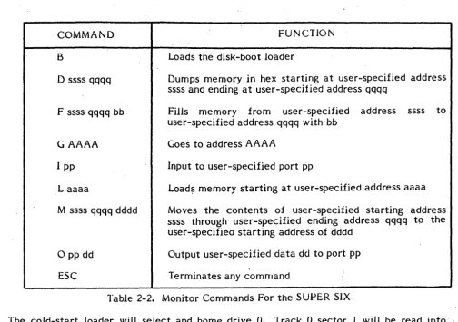
Monitor Commands
COMMAND
B
D ssss qqqq
F ssss qqqq
bb
GAAAA
I
pp
L aaaa
M ssss qqqq dddd
o
pp dd
ESC
FUNCTION
Loads the disk-boot loader
Dumps memory in hex starting at user-specified address
ssss and ending at user-specified address qqqq
Fills memory from
user-specified address ssss to
user-specified address qqqq with bb
Goes to address AAAA
Input to user-specified port pp
Load~
memory starting at user-specified address aaaa
Moves the contents of user-specified starting address
ssss through user-specified ending address qqqq to the
user-specifiea starting address of dddd
Output user-specified data dd to port pp
Terminates any command
Table 2-2. Monitor Commands For the SUPER SIX
The cold-start loader will select and home drive
O.
1 rack 0 sector
1
will be read into
memory at location
o.
Single density is assumed for track
O.
If
an error occures an error
[image:15.618.54.558.27.382.2]2.9.4
Cold Start Program
The cold start program is listed below.
F4B53EOD
F4B7D30C
F4B900
F4BA DBOC
F4BC OF
F4BD DABAF4
F4CO 00
F4Cl 00
F4C200
F4C300
F4C43E03
F4C6030C
F4C800
F4C9DB14
F4CB 00
F4CC OBOC
F4CE E604
F4DO CACCF4
F4D3 AF
F4D46F
F4D567
F4D63C
F4D7 D30E
F4D93E8C
F4DB D30C
F4DD 00
F4DE DB14
F4EO B7
F4El F2EBF4
F4E4 DBOF
F4E677
BOOT 5:
MVI
A,018H
;i<EAO
1
HACK
0
SECTION I INTO
ME.MOHY
OWT
WAIT
;set
double
for 5 inch
BOOT:
MVI
A,ODH
;RESET FDe
OUT
FDC
;ISSUE COMMAND
NOP
FOCW 1:
IN
FOC
;CHECK BUSY
RRC
JC
FDCWI
NOP
;KILL TIME
NOP
NOP
NOP
MVI
A,3
;GET A RESTORE
OUT
FDC
;lSSUI; COMMAND
NOP
IN
WAIT
;WAIT~FORNOP
;INTRQ
TKO:
IN
FDC
ANI
4
;CHECK TRACK 0
JZ
TKO
XRA
A
MOV
L,A
;POIN1 AT LOC 0
MOV
H,A
INR
A
OUT
FDCSEC
;SET SECTOR
MYI
A,08CH
;GET READ COMMAND
OUT
FDC
;lSS':LECOMMAND
NOP
.~I
FDCRD:
IN
WAIT
;WAIT FOR Il'ITRQ
.ORA-
A
;Orr-DR 0
JP
BOOTDN
JE~Jt
IF IN TR
Q
IN
FDCOA T A=
;GE:r
DATA
F4EB OBOC
F4EO 87.
F4EE CAOOOO
F4F 1 F5
F4F2210FF6
F4F5 COE6FO
F4F8 Fl
F4F9 C021Fl
2.10
IN
ORA
JZ
PUSH
LXI
CALL
POP
CALL
BOOTON:
Foe
;CHECK
~lA TUS
A
;0
=
NO ERROR
o
;OK, GO
PSW
;SAVE ERROR
H,BTERR
MSG
;OISK ERROR
PSW
;GET ERROR
THXB
;PRINT IT
RAM ORGANIZATION
The SUPER SIX 128K RAM
is
configured as shown
in
Figure 2-2.
U55
U46
U47
U57
U4B
U56
U5B
U49
U50
U60
U51
U59
U61
U52
U53
U63
U54
U62
Figure 2-2. SUPER SIX RAM Configuration
The
first
64K bank of RAM comprises of U46, U47, U48, U49, U51, U52, U54, U53, and
U50; U46
is
the parity
chip.
2.11
Z80A OMA FEATURES
The Z80A DMA performs transfers, searches and search/transfers on a full-byte basis
in
burst or continuous modes. The cycle length and edge timing can be programmed to
match the speed of any port. A
bit
maskable byte search can be performed
either
concurrently with transfers or as an operation
itself.
2.12
PSNET/IOPERATION
This
paddle card converts TTL to RS232 levels. Pin 6 of the 14
pin
connector on the card
represents TXD; pin 7
is
R TS*; pin 8 is OTR*; pin 5 is CTS*; 1 is DCD* (normally GND); 3
is
RNG* optional; 2
is
OSR*; 4 is RXO. Only pins 3, 5,
20,
2, and I are required for most
printers or CR T's. Printers employing the BUS Y line must be tied to
pin
20 of the OB-25
2.13
PSNET/PAR
This paddle card connects the SUPER SIX parallel
1/0
to a Centronics printer or any other
device that requires buffered signals. Note that a DB-25 connector is used to simplify the
connection for the back panel of the 5-100 system. Thirteen wires are required between
the OB-25 and the printer. A PSN ET IPAR schematic is provided in Appendix M.
2.14
SYNCHRONOU!) OPERATIONS
If
synchronous operation is required, the CTC channels (all four) are unused; the jumper
option on Hand T can be used to bring external clock into the
SlOe
The 1 4
pinconn~ctors(J4 and J5), pins
J
and 11, are not used and can be employed for RNG. SIO pins 13 and 14
are connected
01)the SUPER
~IXboard and must be cut for synchronous operation.
2.15
POWER C0f'.45UMPTION
+8V
+/-16V
2.8 Amp typical
3.1
SECTION III
INPUT/OUTPUT PORTS
INPUT/OUTPUT PORT ASSIGNMENTS
Input/Output port assignments are shown in Table 3-1:
00
01
02
03
04
05
06
07
08
09
OA
OB
OC
OD
OE
OF
10
1 1
12
13
14
15
15
16
17
18
19
lA
IB
ADDRESS
FUNCTION
Read/Write
SIO channel A Data port
Read/Write
SIO channel A status/control port
Read/Write
SIO channel B Data port
Read/Write
SIO channel B status/control port
Read/Write
PIO
cha~nelA Data port
Write
PIO channel B Data port
Read/Write
PIO channel A control port
Write
PIO channel
B
control port
Read/Write
CTC channel 0 control port
Read/Write
CTC channell control port
Read/Write
CTC channel 2 control port
Read/Write
CTC channel 3 control port
Read/Write
FOC command/status port
Read/Write
FDC Track register
Read/Write
FOe sector register
Read/Write
FOC data port
Read/Write
OM A control port
Read/Write
Same as port 10
Read/Write
Same as port 10
Read/Write
Same as port 10
Read/Write
FOe synchronization/Drive/Density
Write
S-IOO bus extended address A 16-A23
Read
On-board Baud Rate jumpers
Write
On-board memory control port 110
Write
On-board memory control port
III
Write
Set Baud Rate
Write
Same as port 18
Write
, Same as port 18
Write
Same as port 18
Table 3-1. I/O Port Assignments for the SUPER
six
Board
Note: All Address in table 3-1 are listed in Hex.
The unused input/output ports are internally
decoded and should ntit be used by external S-IOO
I/O boards.
3.2
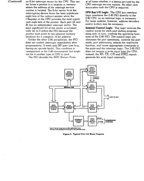
I/O POR T DESCRIPTIO NS
This subsection discribes the function of all
SUPER
SIX
I/O
ports.
3.2.1
Port 00
This read/write port acts as the serial input/output channal A data port and is described in
de"tail in Appendix A.
3.2.2
Port 01
This read/write port acts as the serial input/output channel A status/control port and is
discribed in Appendix A.
3.2.3
Port 02
This read/write port acts as the serial input/output channel B data port and is discribed in
detail in Appendix A.
3.2.4
Port 03
This read/write port acts as the serial input/output channel B status/control port and is
described in detail in Appendix A.
3.2.5
Port 04
This read/write port acts as the parallel input/output channel A data port and is discribed
in detail in Appendix B.
3.2.6
Port 05
This write-only port acts as the parallel input/output channel:g
data
po~tand is
described in detail in Appendix B. This port can be jumpered to the S-IOO vectored
intercept lines onto connector J2 (refer to Section IV).
3.2.7
Port 06
This read/write port acts as the parallel input/output
channel
A
control.
is discribed
in detail
i~Appendix B.
3.2.8
Port 07
This write-only port acts as the parallel input/output channel B control port and is
described. in detail in Appendix B. This port can be jumpered to the S-IOO vectored
interrupt lines onto connector J2 (refer to
~ectionIV).
3.2.10
Port 09
This read/write port acts as the counter/timer circuit channel 1 control port and is
discribed in detail in Appendix C.
3.2.11
Port OA
This read/write port acts as the counter/timer circuit channel 2 control port and is
discribed in detail in Appendix
C.'
3.2.12
Port OB
This read/write port acts as the counter/timer circuit channel 3 control port and is
described in detail in Appendix
C~3.2.13
Port OC
This read/write port acts as the floppy disk control command and status port and is
described in detail in Appendix F.
3.2.14
Port OD
This read/write port acts as the floppy disk control track register port and is discribed in
detail in Appendix F.
'
3.2.15
Port OE
This read/write port acts as the floppy disk control sector register port and is discribed in
detail in Appendix F.
3.2.16
Port OF
This read/write port acts as the floppy disk control data port and is described in detail in
Appendix F.
3.2.17
Ports 10-13
These ports act as direct memory access (OMA) control ports. The Z80A DMA controller
requires only one control/status port; ports 11, 12, and 13 (hex) are ·therefore identical to
port 10 (hex). The floppy disk controller (FOC) data request line is tied to the Z80 DMA
ready input and is active when the signal is high. The OMA controller can move data to
and from the FDC and memory, any I/O channel and memory, or memory and memory, on
or off the board.
*NOTE: All DMA other than FOC must be
started by ready
=
low (e.g., FOC
DRQ
=
low)
3.2.18
Port 14
This
read/write port acts
as
the floppy
rjhk
(~OrltroJlersynchronization, drive
identification, and density port. '
3.2.18.1
Port 14, Write Operation
The two low-order
bits
(DO and
01)
specify the disk drive (see table below). Bit D2
selects the disk head. Bit
03
specifies
the
disk density,
where zero (0)
specifies
single
density and 1
specifies
double
density.
Bit 04 specifies the
disk
drive
size,
where zero (0)
specifies 8-inch disk and
1 specifies 5.25-inch
disk.
The bit
significance is
shown below.
07
=
MSB;
DO
=
LSB
Disk drive select (see table below)
... - -.... Disk
drive select (see table below)
' - - - . H e a d select (O=head 1; l=head 2)
~---.
Disk Density
(O=single; 1 =double)
- - - -.... Size select (0=8 inch;
1=5.25 inch)
---~Not
read
~---~~Not
read
---~Not
read
The two low-order bits (DO and DJ)
specify
the selected
disk
drive, where:
Dl
DO
RESULT
0
0
Disk Drive 0 selected
0
1
Disk
Drive 1 selected
1
0
Disk Drive 2 selected
1
1
Disk
Drive 3 selected
3.2.19,
Port 15
3.2.19.1
Port 15, Read Operation
This port reads the on-board baud rate. The bit significance is shown below.
D7
=
MSB; DO
=
LSB
'Switch 1.
0
=
closed; 1
=
open
... _ _
... Switch 2. 0
=
closed; 1
=
open
...
---_~Switch 3. 0
=
closed; 1
=
open
... - - - .
Switch 4.
0
=
closed; 1
=
open
'---~
Switch 5.
0'
=
closed; 1
=
open
'---~
Switch 6.
0
=
closed; 1
=
open
'---01~
Switch 7. 0
=
closed; 1
=
open
---~
Double sided disk drive status.
o
=
double sidee diskette
3.2.19.2
Note: Jumper J7 specifies the hardware setting for the
baud rate. Port 15 reads jumper J7 to determine the
hardware specified rate.
Port 15, Write Operation
This port controls the S-lOO extended address lines. The bit significance is shown below:
D6
D5
D7
=
MSB; DO
=
LSB
A16
...
--'l~A17'---~
A18
~---.A19 ~---.A20 ---~A21 ---~A22 ---~A23
3.2.20
Ports 16 and 17
These wri te-only ports act as the on-board m.emory control ports zero (0) and 1
respectively. These ports control the on-board memory management circuit, PROM
enable and disable
circ~it,power-on jump reset circuit, and the parity check enable. Port
3.2.20.1
Port· 16, Write Operation
.. The four low-order bits (DO, D 1, D2, and (3) switch the on-board memory
Of\l.
and OFF in
l6K banks. Relative addresses of these banks are as shown below, On hex).
BANK
FROM
TO
DO
0000
3FFF
01
4000
7FFF
D2
8000
BFFF
D3
COOO
FFFF
Bit 5 of
this
port switches the on-board EPROM ON and OFF. This EPROM occupies
addresses FOOD through FFFF (Hex). After the opera ting system
is
loaded the EPROM can
be set to OFF to enable accessing of the RAM addresses FOOD through FFFF (hex); it is
switched to ON Automatically during reset or power-on. This EPROM contains the 510
and FOC initialization code, a simple debugger, and the floppy disk cold-start loader.
Bit D6 resets the power-on jump circuit; it must be reset high before RAM can be
accessed upon completion of a reset or power-on operation.
Bit 07 enables and disables the on-board memory
parity
check latch. On power-up or
reset, this bit is set to low and disables the parity circuit. Prior to enabling the parity
circuit, all memory must be written; this initializes the parity bit for each location.
If
a
parity error occurs an on-board LED
is
turned 0 N.
If
interrupts are enabled and the board
is jumpered for parity error interrupts, the location in error can be located by clearing bit
D7 (to clear the error), resetting the bit,and then reading each location again;
If
no parity
error is encountered it is likely that the error encountered was a soft read error. Parity.
error interrupts can be jumpered to create a non-maskable or counter/timer channel
interrupt.
The bit significance of this port is shown below.'
D7
=
M5B; DO
=
L5B
1
=
Bank ON; 0
=
Bank OFF
Memory bank
0 = 0000 -
3FFF (hex)
... ---l.
Memory bank 1
= 4000 -
7FFF (hex)
~----
... Memory bank 2
= 8000
~BFFF (hex)
- - - -... Memory bank 3
=
COOO - FFFF (hex)
---.Not
read
" - - - .
PROM enabled
=
0;
PROM disabled
=
1
- - - -... Power on jump reset
=
1
3.2.20.2
Port 17, W rite Operation
Bits DO, D
1,
D2, and D3 switch the second 64K set of on-board mernory similarly to the
corresponding bits for port 16. Bits D4, D5, and D6 control memory mapping of the
second set of memory. The first set of 64K bytes is not affected by these settings. Five
memory maps are available and are depicted below. Note that if any 16K segment from
the first bank is selected to overlay a 16K segment frorn the second bank, only the first
bank's 64K memory is selected.
The bit significance of map
a
is shown below. No overlays may be performed on this bank.
I
07
106
l
05
04
03
021 01
I
DO
I
L
p
..
D7 = MSB; DO = LSB
I
= Bank ON;
a
= Bank OFF
Memory bank 4 = 0000 - 3FFF (hex)
Memory bank 5 = 4000 - 7FFF (hex)
Memory bank 6 = 8000 - BFFF (hex)
Memory bank 7 = COO
a -
FFFF (hex)
Set to zero for map zero
Set to zero for map zero
Set to zero for map zero
Not read
The bit significance of map
I
is shown below. Bank zero of the first memory set may
overlay bank 7.
D7 = MSB; DO = LSB
I
= Bank ON;
a
= Bank OFF
Memory bank
4
= 0000 - 3FFF (hex)
---~Memory
bank 5 = 4000 - 7FFF (hex)
- - - .
Memory bank 6 = 8000 - BFFF (hex)
- - - . Memory bank 7=0000-3FFF(hex)-bank
a
' - - - -... Set
to
I
for map
I
---~Set
to zero for map
1
~---
.... Set to zero for map 1
The bit significance of map
2
is shown below. Bank
I
of the first memory set may overlay
bank
6.
07
06
05
04
03
02
01
I
DO
L
_.
-p
D7
= MSB; DO = LSB
I = Bank ON; 0 = Bank OFF
Memory bank 4 = 0000 - 3FFF (hex)
Memory bank
5
= 4000 - 7FFF (hex)
Memory bank 6=4000-7FFF(hex)-bank
1
Memory bank 7 = COOO - FFFF (hex)
Set to zero for map
2
Set to
1 for map 2
Set to zero for map
2
Not read
The bit significance of map 3 is shown below. Banks zero and
I of the first memory set
overlay banks
6
and 7, respectively.
1
07
06
05
D4
D3
D2
I
D
1
I
DO
I
L
p
-D7 = MSB; DO = LSB
1 = Bank ON; 0 = Hank OFF
,Memory bank 4 = 0000 - 3FFF (hex)
Memory bank
5
= 4000 - 7FFF (hex)
Memory bank 6=0000-3FFF(hex)-bank 0
Memory bank 7=4000-7FFF(hex)-bank
I
Set to
I for map 3
Set to I for map 3
Set to zero for map 3
Not read
The bit significance of map 4 is shown below. Bank 3 of the first memory set overlays
bank 4.
I
D7
D61 D5 D41 D31 D21
01
1 DO
I
L
-..
07 = MSB; DO = LSB
1 = Bank ON; 0 = Bank OFF
Memory bank 4=COOO-FFFF(hex)-bank 3
Memory bank 5 = 4000 - 7FFF (hex)
Memory bank 6 = 8000 - BFFF (hex)
Memory bank 7 = COOO - FFFF (hex)
Set to zero for map 4
EXAMPLES OF BANKING:
64K - Bank 0
64K - Bank 1
3
7
2
6
1
5
o
4
Bank a -
Controlled by Port 16
There are five maps possible in Bank 1.
Bank
a
always overrides.
Once a bit in Bank 0
is set, you will
alwa~sget the corresponding
memory
~nthat Bank only.
Bank 1 - Port 17.
Depending on the map used.
M~p
a -
You will get the corresponding memory in Map 0,
Bank 1 if you don't have the Bank
a
bit set.
Map 1 -
If you set bit a , then you will get a-16K,
MAP 0
3/7
2/6
1/5
0/4
MAP
~3
2
~
1/5/7
0/4/6
cooo
·8000
4000
o
MAP 1
3
2/6
1/5
0/4/7
MAP 4
3/4/7
2/6
1/5
o
MAP 2
3/7
2
1/5/6
EXAMPLES OF BANKING:
64K -
Bank 0
64K -
Bank 1
3
7
2
6
1
5
o
4
Bank 0 -
Controlled by Port 16
There are five maps possible in Bank 1.
Bank 0 always overrides.
Once a bit in Bank 0
is set, you will always get the corresponding
memory in that Bank only.
Bank 1 -
Port 17.
Depending on the map used.
M~p
0 - You will get the corresponding memory in Map 0,
Bank 1 if you don't have the Bank 0 bit set.
Map 1 -
If you set bit 0 , then you will get 0-16K,
if you set just bit 3 , then you get 0-16K
MAP 0
3/7
2/6
1/5
0/4
MAP
~3
2
1/5/7
0/4/6
cooo
8000
4000
o
MAP 1
3
2/6
1/5
0/4/7
MAP 4
3/4/7
2/6
1/5
o
MAP 2
3/7
2
1/5/6
EXAMPLES OF BANKING:
64K - Bank 0
64K - Bank 1
3
7
2
6
i
5
o
4
Bank 0 - Controlled by Port 16
There are five maps possible in Bank 1.
Bank 0 always overrides.
Once a bit in Bank 0
is set, you will always get the corresponding
memory in that Bank only.
Bank 1 - Port 17.
Depending on the map used.
M~p
0 - You will get the corresponding memory in Map 0,
Bank 1 if you don't have the Bank 0 bit set.
Map 1 -
If you set bit 0 , then you will get 0-16K,
if you set just bit 3 , then you get 0-16K
MAP 0
3/7
2/6
1/5
0/4
MAP
~3
2
...-1/5/7
0/4/6
cooo
8000
4000
o
MAP 1
3
2/6
1/5
0/4/7
MAP 4
3/4/7
2/6
1/5
o
MAP 2
3/7
2
1/5/6
3.2.21
Port
18
This write-only port acts as the set-baud-rate port and allows the user to perform a
software reset of the baud rate for SIO channels A and B. The bit significance of this port
is show.n be low.
07
=
MSB; DO
=
LSB
SIO channel A baud bit A
... ----I~
SIO channel A baud bit B
" - - - . SIO channel A baud bit C
'---~
SIO channel A baud bit D
' - - - -... SIO
channel B baud bit A
---~~SIO
channel B baud bit B
~---
. . SIO channel B baud bit C
"---~SIO
channel B baud bit D
The baud rates equated with bit settings A, B, C, and D are shown in Table
3-2.
These are
identical for both channel A and channel B.
BIT
BIT
BIT
BIT
BAUD
D
C
B
A
RATE
a
0
0
a
50
a
0
0
1
75
a
0
I
a
110
a
0
1
1
134.5
a
I
0
a
150
a
1
0
1
300
a
1
1
a
600
a
I
1
1
1200
I
0
a
a
1800
I
0
a
1
2000
1
0
1
a
2400
1
a
1
I
3600
1
1
a
a
4800
1
1
a
1
7200
I
1
1
a
9600
1
I
1
I
19,200
4.1
SECTION IV
JUMPER CON N ECTIONS
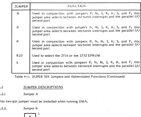
JUMPER DEFINITIONS
Table
4-1
presents the avaiJable jumpers and abbreviates their assigned functions.
Detailed descriptions of individual jumper functions are presented following this table. To
facilitate jumper insertion, each three (or more) pin jumper is depicted in an illustration
contained within the narrative for that jumper.
JUMPER
FUNCTION
A
Generates Wait States
8
Selects between on-board Tri-state and S-IOO bus buffering
(MWRITE)
c
D
E
F
G
H&T
J
J6
J7
K
M
Selects 6MHz or 4MHz operation
Selects 6MHz or 4MHz operation
For DMA ONLY {2-3}
Selects between the S-lOO bus interrupt
(IN T)
and the vectored
interrupt zero (VIO)
Used in conjunction with jumpers P, N, M, K, R, S, and J, this
jumper area selects between vectored interrupts and the paraUel I/O
second port
Used in adjusting the floppy disk controller phase line level
(PLL)
This jumper area selects synchronous or asynchronous serial I/O
Used in conjunction with jumpers P, N, M, K, R, S, and F,
this
jumper area selects between vectored interrupts and the parallel
I/0
second port
Used for interrupts of the eTC to 1.5 MHz, DMA or parity error,
NMI
or INTRQ
Used to set the hardware baud rate
Used in conjunction with jumpers P, N, M, J, R, S, and F, this
jumper area selects between vectored interrupts and the parallel
I/0
second port
4.2
4.2.1
JUMPER
rU~Cl I()~N
Used in conjunctior,
with
jUfrlper~£1,
:'vi,
J, K, k,
~,and F, this
jumper Cired.
~€:lect~
b(::twe€:fl vectored interrupts d.nd the parallel 1/0
second port
P
Used
in conjunction with jumpers
i\,
M, J, K, R, 5, and
F,
this
jumper area selects between vectored interrupts and the parallel I/0
second port
R
Used in conjunction with jumpers P, N, M, J, K, S, and F, this
jumper area selects between vectored interrupts and the parallel 1/0
second port
R25
Used to select the
2716
or the 2732 EPROM
S
Used ,in conjunction with jumpers P, N, M, J, K, R, and F, this
jumper area selects between vectored interrupts and the parallel I/0
second port
Table 4-1. SUPER SIX Jumpers and Abbreviated Functions (Continued)
JUMPER DESCRIPTIONS
Jumper A
This two-pin jumper must be installed when running DMA.
4.2.2.
Jumper B
0~
When installed
this
two-pin jumper causes buffering of the M W RITE signal to be
performed through the on-board tri-state buffer.
When not installed, buffering is
performed through the 5-100 bus. In most cases this jumper is installed.
4.2.3
Jumper C
1
2
3
[image:35.618.65.543.33.432.2]4.2.4
Jumper D
1
·2
3
When installed between 1 and 2,
this
jumper sets the board for 6MHz operation. When
installed between 2 and 3, 4MHz operation is specified. Also see jumper C, above.
For DMA
Operation
plug
between 2-3 always.
4.2.5
Jumper E
1
2
3
This jumper
determines
whether the 5-100 bus interrupt (IN
T)
or the vectored interrupt
zero (VIa)
is
to be used. When installed between
pins
1 and 2, the VIa is tied to priority
interrupt DAIS Y CHAIN.
W
hen installed between pins 2 and
3,
the priority interrupt
(5-100 pin 73) is tied to the interrupt DAISY CHAIN.
4.2.6
Jumper
G
This jumper adjusts the floppy disk controller phase-locked loop (PLL) and is not installed
unless adjusting the PLL.
4.2.7
Jumpers Hand T
This jumper area specifies that serial I/O is to be performed synchronously or
asynchronously. When installed between pins 1 and 2 of jumpers Hand T, synchronous
operation is selected; when installed between pins 2 and 3, asynchronous operation is
selected. Pins 1 and 11 of the 14 pin J4 and J5 connectors are not factory connected.
These may be used in synchronous operations to bring the external clock or ring indicator
into the 510.
4.2.8
Jumper J6
· 4.2.9
This! jumper allo\\·s selection
b~t\\"('('nth(, 271
band2732
EPRL)Ms.
When installed
between pins I and
2,
the 2716
tPR~"'~'is
~H1dresst~d;when installed
b~tweenpins
2.
and 3,
the 2732 EPROM is addressed.
4.2.10
GND
GND
GND
GND
GND
GND
GND
Jumper J7
8
7
9
6
10
5
.
-11
4
12
"3
13
2
14
·1
BOo
BOS
BD4
BD3
BD2
BDl
BOO
This jumper sets the hardware baud rate. When the jumper is inserted an inverted ground
condition exists
(l);
when not inserted a zero
(0)
value is assumed. This setting must agree
with the Set Baud Rate Port (port
18 -
refer to subsection 3.2.20 e.g., when 7, 6, 5, and 4
are installed, 19.2K baud is read.
4.2.11
Jumpers P, N, M, K, J, R, 5, and F
p
N
M
K
J R 5
1---+----+----1
F
These jumpers select between vectored interrupts or the Parallel 1/0 second port. When
installed between pins
1
and 2, the vectored
int~rruptszero
(0)
to 7, as selected, are
4.3
FACTORY AND OEM INSTALLED JUMPERS
4.3.1
8-Inch Floppy Disk Drive
Install jumpers as indicated below.
4.3.2
JUMPER BETWEEN PINS
FUNCTION
B
C
D
E
H
T
J6
J7
P
N
M
K
J
R
S
F
1 - 2
2-3
1 - 2
2 -
3
2 - 3
]·~·J4'