March CRF: an Efficient Test for Complex Read Faults
in SRAM Memories
Luigi Dilillo
Bashir M. Al-Hashimi
University of Southampton - Electronics and Computer Science (ECS) Department Mountbatten Building, Highfield, Southampton, SO17 1BJ, United Kingdom
Tel.: +44 (0)23 8059 3119 Fax: +44 (0)23 8059 2901
Email: (L. Dilillo) [email protected] (B. M. Al-Hashimi) [email protected]
Abstract:
In this paper we study Complex Read Faults in SRAMs, a combination of various
malfunctions that affect the read operation in nanoscale memories. All the memory elements involved
in the read operation are studied, underlining the causes of the realistic faults concerning this
operation. The requirements to cover these fault models are given. We show that the different causes
of read failure are independent and may coexist in nanoscale SRAMs, summing their effects and
provoking Complex Read Faults, CRFs. We show that the test methodology to cover this new read
faults consists in test patterns that match the requirements to cover all the different simple read fault
models. We propose a low complexity (
∼
2N) test, March CRF, that covers effectively all the realistic
Complex Read Faults
Keywords:
SRAM, Nanoscale Technologies, Read Operation, Realistic Faults, Complex Read Faults,
March test.
Proposed Topic:
Memory and processor test.
Corresponding author
Dr Luigi DILILLO
University of Southampton - Electronics and Computer Science (ECS) Department Building 86, Highfield, Southampton, SO17 1BJ, United Kingdom Email: [email protected] URL: http://www.lirmm.fr/~dilillo
Proposed to
X Workshop on Design and Diagnostics of Electronic Circuits and Systems
Krakow, Poland
March CRF: an Efficient Test for Complex Read Faults
in SRAM Memories
Luigi Dilillo
Bashir M. Al-Hashimi
University of Southampton - Electronics and Computer Science (ECS) Department Mountbatten Building, Highfield, Southampton, SO17 1BJ, United Kingdom Email: (L. Dilillo) [email protected] (B. M. Al-Hashimi) [email protected]
Abstract
In this paper we study Complex Read Faults in SRAMs, a combination of various malfunctions that affect the read operation in nanoscale memories. All the memory elements involved in the read operation are studied, underlining the causes of the realistic faults concerning this operation. The requirements to cover these fault models are given. We show that the different causes of read failure are independent and may coexist in nanoscale SRAMs, summing their effects and provoking Complex Read Faults, CRFs. We show that the test methodology to cover this new read faults consists in test patterns that match the requirements to cover all the different simple read fault models. We propose a low complexity (∼2N) test, March CRF, that covers effectively all the realistic Complex Read Faults.
1
Introduction
Embedded memories are dominant in future SoCs and, as predicted by the ITRS Roadmap, such devices will reach a density of approximately 95% of the total area in ten years [1]. As a result, the SoCs yield will depend largely on memories and the development of efficient test solutions and repair schemes for memories will be essential. Most of memory tests rely on classic fault models such as stuck at fault, coupling fault and transition fault. Although these fault models are still valid, there is a new class of faults, called dynamic, that is emerging in nanoscale memories. Such faults need complex patterns to be sensitized. The emergence of these new fault models is due to factors related the latest technologies. In particular, resistive defects are becoming very common in nanoscale technologies, especially in proximity of interconnections and vias, as reported by INTEL in [2]. Resistive defects cause delay faults and dynamic faults that are difficult to sensitize [3, 4]. Other types of faults are also emerging and are caused by leakage currents and electrical parameter fluctuations, as transistor threshold voltage Vt, within the
same die [5]. These faults affect mainly structures with high symmetry as memories.
In the paper, we refer to SRAM read faults as Read Faults (RFs), irrespectively of the cause. All the memory elements that are involved in the read operation can be affected by electrical failure, resulting in RFs: the core cells and word lines [6], the bit lines[7, 8], the pre-charge circuits [9], the sense amplifiers [10, 11]. Previous papers have targeted RFs due to a single electric cause and the proposed detection algorithms are effective over certain fault threshold. For example, certain algorithms cover RFs
due to resistive open defects when the equivalent resistance is above a certain value; other algorithms cover RFs due to variation of Vt when this parameter fluctuates
over a certain percentage. We show that the collective action of different contributions to RFs may induce the read operation to fail, even when these contributions are individually not sufficient to generate malfunctions. These faults can be modelled as Complex Read Faults (CRFs) and in this paper we propose a test methodology to cover CRFs, and for this aim we introduce the algorithm March CRF.
The rest of the paper is organized as follows. In Section 2, we describe the read operation in SRAMs. In Section 3, we present the various fault models concerning the read operation and the electric phenomena that they model. The test methodology and algorithm to cover the Complex Read Faults are presented in Section 4. Conclusions are given in Section 5.
2
Background: SRAM read operation
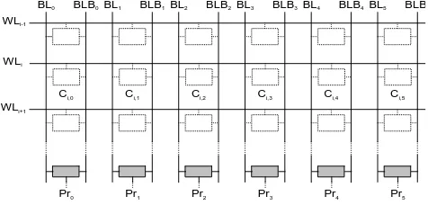
In this section we describe the read operation in SRAM memories in order to facilitate the presentation of the mechanisms that involve Read Faults. In the SRAM memory array (see Figure 1), there is a pre-charge circuit (Pr) for each column, which is used to set the voltage level of the two bit lines of the column (BL and BLB) at a fixed value - VDD for most SRAM memories. This action is necessary for a correct read operation.
Ci,0 Ci,1 Ci,2 Ci,3 Ci,4 Ci,5
WLi-1
WLi+1
BL0 BLB0BL1 BLB1BL2 BLB2 BL3 BLB3 BL4 BLB4BL5 BLB
WLi
[image:2.595.309.547.513.627.2]Pr0 Pr1 Pr2 Pr3 Pr4 Pr5
Figure 1: A portion of a cell array with pre-charge circuits
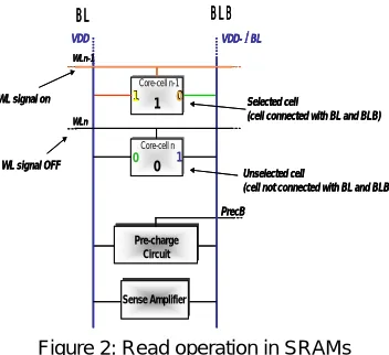
When a read operation is acted on a certain cell, the pre-charge circuit is turned OFF on the two bit lines belonging to the cell. At this point, these bit lines are floating and charged at VDD and the read operation can start. Figure 2 shows a memory column with two cells, the pre-charge circuit and the sense amplifier. As an example, we perform a read operation on the top cell that stores a ‘1’. The read operation begins when the word line enable signal (WLn-1)
Core-cell n-1
Pre-charge Circuit
PrecB WLn
Core-cell n
1
0
VDD VDD-∆BL
Sense Amplifier 1
0
1
1 00
BLB BL
Unselected cell
(cell not connected with BL and BLB) Selected cell
(cell connected with BL and BLB)
WL signal OFF WL signal on
WLn-1
Core-cell n-1
Pre-charge Circuit
PrecB WLn
Core-cell n
1
0
VDD VDD-∆BL
Sense Amplifier 1
0
1
1 00
BLB BL
Unselected cell
(cell not connected with BL and BLB) Selected cell
(cell connected with BL and BLB)
WL signal OFF WL signal on
WLn-1
Core-cell n-1
Pre-charge Circuit
PrecB WLn
Core-cell n
1
0
VDD VDD-∆BL
Sense Amplifier 1
0
1
1 00
BLB BL
Unselected cell
(cell not connected with BL and BLB) Selected cell
(cell connected with BL and BLB)
WL signal OFF WL signal on
[image:3.595.80.256.68.229.2]WLn-1
Figure 2: Read operation in SRAMs
The cell stores a ‘1’, thus the left node is at ‘1’, i.e. VDD, while the right node is at ‘0’, i.e. 0V. During the read operation, the bit line on the left side remains at VDD because it is connected with the node of the cell at VDD, while the bit line on the right side, BLB, is connected with the node of the cell at ‘0’ and is partially discharged, reaching the voltage level VDD-∆BL. A sense amplifier detects this different voltage level (∆BL= VBL-VBLB)
between the two bit lines and gives the output value, ‘1’. For a correct read operation ∆BL is about VDD/10 or more. The read value would be ‘0’ in the opposite case when a cell storing a ‘0’ is selected, BL is partially discharged at VDD-∆BL and BLB stays at VDD. The above description shows that, for a correct read operation, the two bit lines connected to the selected cell need to be fully charged and equalized at VDD, otherwise erroneous values may be obtained during the read operation. In the next section, we show in detail how different electric causes can lead the failing of the read operation in SRAMs.
3
Analysis of realistic Read Faults
In this section we describe with some detail the causes of RFs in SRAM. In the previous section we have described the read operation in SRAM. In that description we can identify different main elements that are responsible of the operation:
− The core-cell, where the information is stored;
− The word line that carries the signal enabling the cell selection for the read operation;
− The bit lines that represent the wires that allow the exchange of the data to and from the core-cell through the cell pass transistors;
− The pre-charge circuit that sets the voltage level at VDD of the bit lines in order to ensure a correct read operation;
− The sense amplifier that amplifies the read value from the bit lines to the output.
These elements can be affected in different ways producing an influence on the read operation as we show in the following sub sections.
3.1 The core-cell and word line
A typical SRAM cell has six transistors, see Figure 3, organized as two inverters connected in a loop (Tn1+Tp1 and Tn2+Tp2) and two pass transistors (Tn3 and Tn4) that
connect the cell with the two bit lines. In [6], it is shown that the presence of resistive open defects may lead to different faults depending of their placement, see Figure 3.
VDD
VDD
WL
BLB BL
Tp1
Tn1
Tp2
Tn2
Tn4 Tn3
S
SB Df4
Df3 Df2
Df6
Df1 Df5
INV1
INV2
Figure 3: SRAM 6T cell with injected resistive defects
The faults models, induced by the injected defects, are Transition Fault (TF, defects Df1, Df5 and Df6), Read Destructive Fault (RDF, defects Df2 and Df3), dynamic Read Destructive Fault (dRDF, defects Df2, Df3 and Df4), Deceptive Read Destructive Fault (DRDF, defects Df2 and Df3) and Incorrect Read Fault (IRF, defect Df5). Note that in this study we take in account only non-destructive read failures, i.e. all those RFs that do not carry modification of the information stored in the cells (the selected cell stores the correct value, but the read value is incorrect). Thus, we focus on the IRFs that are caused by defect Df5. This defect represents the equivalent resistive effect of long connections wires as the word lines are. The IRF occurs because the read operation needs a certain minimal time to be performed. During this operation the nodes S and SB are connected to the bit lines BL and BLB by the pass-transistors Tn3 and Tn4. The defect involves a delay in the switching ON of these two transistors reducing the operative time of the read operation. The requirement to detect this fault is the following:
a1. At least a cell for each row of the memory array needs to be accessed for a (write and) read operation; the data stored is not relevant for the fault detection, i.e. the data to be written and read could be ‘0’ or ‘1’.
3.2 The bit lines and cell pass transistors
Tn3 Tn2
Tn1 Tp2
Tp1
S SB
Tn4
WLn= 0V
BLB BL
0 1
VDD VDD
UNSELECTED CELL
UNSELECTED CELL
Tn3 Tn2
Tn1 Tp2
Tp1
S SB
Tn4
WLn= 0V
BLB BL
0 1
VDD VDD
UNSELECTED CELL
UNSELECTED CELL
Tn3 Tn2
Tn1 Tp2
Tp1
S SB
Tn4
WLn= 0V
BLB BL
0 1
VDD VDD
UNSELECTED CELL
UNSELECTED CELL
Tn3 Tn2
Tn1 Tp2
Tp1
S SB
Tn4
WLn= 0V
BLB BL
0 1
VDD VDD
UNSELECTED CELL
[image:4.595.93.248.63.198.2]UNSELECTED CELL
Figure 4: Leakage currents through the pass transistors in an unselected cell
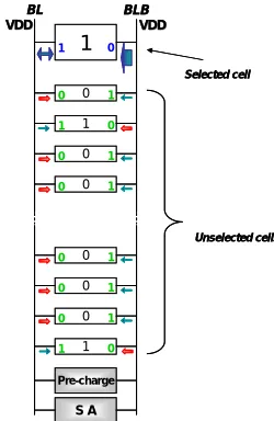
When the cell is unselected, the Word Line selection signal is low (WLn=0) and the two pass transistors are OFF. Although the pass transistors are OFF, there is a certain amount of current that leaks through these two transistors discharging the bit lines. In particular, the leakage current that concerns transistor Tn3 has three components: 1. Subthreshold leakage current that flows from bit line BL, charged at VDD, to transistor Tn3 substrate that is polarised at 0V. 2. Gate leakage current that flows from bit line BL, charged at VDD, through the gate oxide, to the gate of transistor Tn3 that is at 0V (cell not selected). 3. Junction leakage current that flows from bit line BL, charged at VDD, to node S of the cell that is at 0V. In nanoscale technologies the three components that compose the total leakage current are becoming more important with the reduction of the transistor size and the thickness of the gate oxide [12]. Note that for transistor Tn4 the junction leakage current (3.) is not present because the cell node SB has the same voltage level (VSB=VDD) of bit line BLB.
The consequence is that in an unselected cell the leakage currents from the bit lines through the two pass transistors are not symmetric. In particular the leakage is higher on the side with the cell node at ‘0’, e.g. on the left side as in Figure 4. In practice, an SRAM memory column has hundreds of cells and only one cell at a time can be selected for the read operation. Each unselected cell of the column interacts with the bit lines BL and BLB, because of the leakage currents, see Figure 5. The leakage currents drawn by each unselected cell affect the voltage difference observed by the sense amplifier during the read operation causing Leakage Read Faults. The definition of Leakage Read Fault for SRAM memories is the following:
LRF: Leakage Read Fault – When in a memory
column most cells store the same value X∈{0,1}, the leakage currents, through the pass transistors of the unselected cells may affect the read operation in the cells storing the value X , where X is the opposite of X: X is expected and X is read.
In order to identify the relation between the values stored in the cells of the column and the LRF occurrence, we have performed Spice simulation on a 1024x1024 SRAM memory using the 65nm Berkley Predictive Technology models [13].
1
1 0
0
0 1
1
1 0
0
0 1
0
0 1
0
0 1
0
0 1
0
0 1
1
1 0
S A VDD
VDD VDDVDD
Pre-charge
Selected cell
Unselected cells
BL BLB
1
1 0
0
0 1
1
1 0
0
0 1
0
0 1
0
0 1
0
0 1
0
0 1
1
1 0
S A VDD
VDD VDDVDD
Pre-charge
Selected cell
Unselected cells
BL BLB
1
1 0
0
0 1
1
1 0
0
0 1
0
0 1
0
0 1
0
0 1
0
0 1
1
1 0
S A VDD
VDD VDDVDD
Pre-charge
Selected cell
Unselected cells
[image:4.595.366.491.68.260.2]BL BLB
Figure 5: The leakage effect in a memory column
These simulations have shown that LRFs are more likely to appear in the following conditions: low voltage supply, high temperature and high frequency. The configurations and conditions useful for the sensitization and observation of LRFs are summarized in the following three test requirements:
b1. In the column composed of m cells, m-1 cells have to store the same value X∈{0,1} and one cell has to storeX , where X is the opposite of X;
b2. When the requirement a. is satisfied, a read operation is performed in the cell storing X (=rX).
b3. The requirement a. and b. have to be verified for all the columns in the memory array and for both logic values of X.
The first requirement (b1.) is necessary for the sensitization of the LRF, while the second requirement (b2.) is necessary for both sensitization and observation of the LRF. The third requirement (b3.) is necessary because in nanoscale technologies there are often fluctuations of different parameters, and in particular Vt, within the die
[5]. Thus, in the same memory array, there can be columns that present LRFs and fault free columns. Consequently, the test pattern needs to be run in all the columns of the memory array.
3.3 The pre-charge circuit
A typical pre-charge circuit is depicted in Figure 6.
PrecB Mtp2
Df1 BLB BL
Df5 Df4
VDD
Mtp3
Mtp1 Df2
[image:4.595.313.520.596.704.2]Df3
Figure 6: Pre-charge circuit with injected resistive defects
Transistor Mtp1 connects the two bit lines for their equalization. When one of the two bit lines is already at VDD, Mtp1 helps the pull-up of the other bit line.
In the normal operation of the memory, the pre-charge circuit is most of the time activated and its action is to set the voltage level of each couple of bit lines at a certain value, VDD for most of SRAM memories. The fact that each couple of bit lines, BL and BLB, is exactly at VDD level is required for a correct read operation, as explained above. For this reason the pre-charge circuit has not only Mtp2 and Mtp3 that feed their relative bit lines with a pull-up effect, but also transistor Mtp1 that ensure the perfect equalization of the two bit lines. In [9] the influence of injected resistive open defects (see Df1, Df2,… in Figure 6) on the pre-charge circuit function is studied. Spice simulations show that the pre-charge circuits are sensible only to defects Df1 and Df5. Defect Df2 involves an incorrect pull-up of the bit lines, that does not disturb enough the read operation, because, even if the VDD is not reached there is a good equalization. In presence of Df3 and Df4, at the end of the pre-charge action there is an incorrect ∆BL, which is not large enough to imply a faulty behavior of the memory. The defects Df1 and Df5 cause RFs that are modelled with two fault models called URWF (Un-Restored Write Fault) and URRF (Un-Restored Read Fault) that have the following definitions:
Un-restored Write Fault (URWF): the pull-up of the two bit lines is not completely acted after the state reached with a write operation. Consequently the following read operation of an opposite data in a cell of the same column is not correctly acted.
Un-restored Read Fault (URRF): the pull-up of the two bit lines is not completely acted after the state reached with a read operation. Consequently the following read operation of an opposite data in a cell of the same column is not correctly acted.
As example, in Figure 7 we report the waveforms obtained after the simulations of the detection sequences for URRF (r0 on cell Cx followed by r1 on cell Cy of the same column) and URWF (w0 on cell Cx followed by r1 on cell Cy on the same column), with the pre-charge circuit affected by defect Df1 of the same resistive value.
w0 on cell Cx
Incorrect r0 on cell Cy of the same
column (‘1’ was expected)
incomplete pull-up of BL
BL BLB
TIME (s)
6n 8n 10n
1.5
1.0
0.5
0.0
r0 on cell Cx Incorrect r0 of cell C
y on the same
column (‘1’ was expected)
Incomplete pull-up of BL
CLK
BL
BLB 1.5
1.0
0.5
[image:5.595.346.489.525.707.2] [image:5.595.57.284.568.727.2]0.0
Figure 7: Simulation with defect Df1 in the pre-charge circuit: URRF and URWF
In both cases, we can easily observe the incomplete pull-up of the pre-charge circuit: in the upper case we have
an URRF because the first operation is r0; in the other case we have an URWF because the first operation is w0. The incomplete pull-up involves in both cases an incorrect read operation: ‘1’ is expected but ‘0’ is actually read. These two fault models can be classified as dynamic faults, because their sensitization needs two operations in sequence. The test requirements to detect them can be summarized as follow:
c1. (URWF): In a memory column, a write operation wX is to be performed on a cell Ca immediately followed by read operation rXon another cell Cb of the same column, with X∈{0,1} and X is the opposite of X. This requirement has to be verified for all the columns in the memory array and for both logic values.
c2. (URRF): In a memory column, a read operation rX is to be performed on a cell Ca immediately followed by read operation rXon another cell Cb of the same column, with X∈{0,1} andXis the opposite of X. This requirement has to be verified for all the columns in the memory array and for both logic values.
In [9] is demonstrated that the test patterns c1 to cover URWFs are more effective than those covering URRFs, i.e. the requirement useful to detect URWFs include the one to detect URRFs.
3.4 The sense amplifier
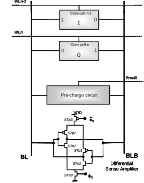
Sense amplifiers have a key role in the read operation and a variety of designs are in use, some of which closely resemble the design of an SRAM core-cell. During the read operation, the memory cell provides a differential output voltage on the two bit lines, BL and BLB that needs to be amplified. This signal is of the order of VDD/10 and is applied to the input terminals of the sense amplifier. The sense amplifier in turn responds by providing a full logic-swing (0 to VDD) signal at its output terminals. Figure 8 depicts a typical structure of the sense amplifier, with some of the other column circuitry of an SRAM, in particular two-core cells and the pre-charge circuit.
Core-cell n-1
Pre-charge circuit
Differential Sense Amplifier
WLn
WLn--11
PrecB
PrecB
WLn
WLn
Core-cell n 1
0 1
1 0
0
VDD
φS
φS
BLB BL
Core-cell n-1
Pre-charge circuit
Differential Sense Amplifier
WLn
WLn--11
PrecB
PrecB
WLn
WLn
Core-cell n 1
0 1
1 0
0
VDD
STp2
STn2 STp1
STn1
φS
φS STp3
STn3
BLB BL
Core-cell n-1
Pre-charge circuit
Differential Sense Amplifier
WLn
WLn--11
PrecB
PrecB
WLn
WLn
Core-cell n 1
0 1
1 0
0
VDD
φS
φS
BLB BL
Core-cell n-1
Pre-charge circuit
Differential Sense Amplifier
WLn
WLn--11
PrecB
PrecB
WLn
WLn
Core-cell n 1
0 1
1 0
0
VDD
STp2
STn2 STp1
STn1
φS
φS STp3
STn3
BLB BL
Figure 8: a differential SA connected to the bit lines
the other by transistors STp2 and STn2. Transistors STp3 and STn3 act as switches that connect the sense amplifier to VDD and ground only when data-sensing action is required. The signal φs and its complementary φs
command the action of the sense amplifier. The amplifier is required to detect a small signal appearing between BL and BLB, and to amplify it to provide a full-swing signal at BL and BLB
Functional failure in the action of the sense amplifier may be caused by two principal factors. The first factor is the presence of resistive defects inside the circuit, as seen for the core-cell, and the second one is the variation of the threshold voltage Vt of the transistors that compose the
sense amplifier [10, 11]. In both cases, the effect is an unbalanced amount of current in the two sides of the amplifier prior the sensing. This causes an offset voltage that modifies the voltage difference between the bit lines (∆BL) generated by during the read operation. The requirement to detect this RF is the following:
d1. At least a cell for each column of the memory array needs to be accessed for a (write and) read operation with both the logic values: r0 and r1.
Note that the sense amplifiers are more prone to be faulty in nanoscale SRAM. When smaller transistors are used in the sense amplifier, a higher differential voltage (∆BL) is needed before the sense amplifier is latched [10]. This implies that, any reduction of the read ∆BL prior the sensing stage is aggravated when the sense amplifier is composed by small transistors.
4
Testing Complex Read Faults
Now, we consider the various RFs presented in the previous section, showing that the causes of different fault models may coexist and sum their effects. The existing algorithms target only one RF model at time and are effective only above a certain fault threshold. The simultaneous presence of multiple causes of RFs, below the detection threshold, may lead to read malfunctions, due to the cumulative effect. This means that in order to test efficiently the RFs it is useful to consider the combination of all the requirements to cover the different RFs. In nanoscale technologies the occurrence of resistive open defects is more and more frequent because of the reduction of the wires dimension, their reduced thickness and for the presence of a high number of vias between the multiple levels of metal [2]. At same time, leakage currents are a constant relevant factor for technology <90nm, with drawback in terms of power consumption [14, 15] and reliability [7], imposing new solutions in terms of design [8]. These factors are the direct causes of the RF faults as we have exposed in Section 3, and for their nature may coexist summing their effects, resulting in Complex Read Faults. If the presence of multiple resistive defects are unlikely to appear in a relative small region of the die, the effects on the read operation, due to a single defect in the core cell (or pre-charge circuit or sense amplifier), are certainly to be summed to the effects of the leakage currents, always massively present in technologies ≤90nm. The same observation can be done for sense amplifier
dissymmetry, caused by Vt variations and that can sum its
effect on the read operation to those brought by leakage currents and/or resistive defects. The consequence is that in nanoscale SRAM the read faults can hardly be associated to a single electric origin, but they need to be treated as Complex Read Fault. In order to generate an efficient test methodology to cover the Complex RFs, it is necessary to match all the requirements to cover all the exposed read fault models at same time. The combination of all the various test requirements for each simple RF model (see Section 3) can be resumed in following points:
1. At least a cell for each row of the memory array needs to be accessed for a write and read operation; the data stored is not relevant for the fault detection, i.e. the data to be written and read could be ‘0’ or ‘1’.
2. In the column composed of m cells, m-1 cells have to store the same value X∈{0,1} and one cell has to storeX, where X is the opposite of X;
3. When the requirement a. is satisfied, a read operation is performed in the cell storing X (=rX).
4. The points 2. and 3. have to be verified for all the columns in the memory array and for both logic values.
5. In a memory column, a write operation wX is to be performed on a cell Ca immediately followed by read operation rXon another cell Cb of the same column, with X∈{0, 1} and X is the opposite of X. This requirement has to be verified for all the columns in the memory array and for both logic values.
The first requirement is to cover the RFs connected to electrical malfunctions (presence of resistive open defects) in word line and the core cell. The following three requirements were expressed to cover the RFs connected to leakage currents from the bit lines through the cell pass transistors. These requirements include those necessary to cover the RFs connected to sense amplifier, as well it does the requirement 5, useful to cover IRFs connected to resistive defects in the pre-charge circuit.
On the base of the requirements to cover Complex RFs, we propose a March like test, named March CRF, which allows the best coverage of read faults in SRAM memories, because it takes in account multiple electric causes. This test algorithm is depicted in Figure 9.
( ) ( )
w1
iw0
all-{i,i±1};
⇑
( ) ( )
w0
i±1r1
i;
⇑
M0 M1
( ) ( )
w0
iw1
all-{i,i±1};
⇓
( ) ( )
w1
i±1r0
i⇓
M2 M3
Figure 9: March CRF
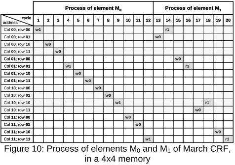
In order to make easier the understanding of March CRF, we perform its first two elements M0 and M1 (the other
Process of element M1
Process of element M0
r1 20
w0 19
w1 Col 11; row 11
Col 11; row 10
w0 Col 11; row 01
w0 Col 11; row 00
w0 Col 10; row 11
r1 w1
Col 10; row 10
w0 Col 10; row 01
w0 Col 10; row 00
w0 Col 01; row 11
w0 Col 01; row 10
r1 w1
Col 01; row 01
w0 Col 01; row 00
18 17
w0 Col 00; row 11
w0 Col 00; row 10
w0 Col 00; row 01
r1 w1
Col 00; row 00
16 15 14 13 12 11 10 9 8 7 6 5 4 3 2 1 cycle address
Process of element M1
Process of element M0
r1 20
w0 19
w1 Col 11; row 11
Col 11; row 10
w0 Col 11; row 01
w0 Col 11; row 00
w0 Col 10; row 11
r1 w1
Col 10; row 10
w0 Col 10; row 01
w0 Col 10; row 00
w0 Col 01; row 11
w0 Col 01; row 10
r1 w1
Col 01; row 01
w0 Col 01; row 00
18 17
w0 Col 00; row 11
w0 Col 00; row 10
w0 Col 00; row 01
r1 w1
Col 00; row 00
[image:7.595.49.287.64.232.2]16 15 14 13 12 11 10 9 8 7 6 5 4 3 2 1 cycle address
Figure 10: Process of elements M0 and M1 of March CRF,
in a 4x4 memory
The element M0 operates a w1 in the ith cell of each
column and w0 in all the cells of the column, excluded the ith and the (i±1)th (i+1 for the columns with even address and i-1 for the columns with odd address). The index i∈{0, 1, 2, …, n}, where n is the number of columns in the memory array; i increases of one unit at the end of each march element process in a column operation. The element M1 operates a w0 in the (i±1)th cell and r1 the ith cell. The
following two elements do the same operations inverting the written and read data.
From the process partially shown in the diagram in Figure 10 (elements M0 and M1), we can verify that the
March CRF matches all the requirements needed to cover the Complex Read Faults, affecting SRAM memories. In fact, in each column the ‘X’ is written in all the cells but one where ‘X’ is written and read: requirements 2, 3 and 4. For each column, a wX operation is acted immediately followed by an rXoperation: requirement 5. Note that the requirements are completely accomplished because elements both value of X∈{0,1} are used. Concerning requirement 1, it is always accomplished (a write and read operation for each row) when m≤2n, i.e. for all the memory arrays where the number of rows is smaller than twice the number of columns. For memory array in which m>2n (number of rows more than double than number of column), further read operation can be added to match requirement 1.
The complexity of the algorithm March CRF is very low: 2N+2n (∼2N), where N is the number of cells and n is the number of columns in the memory. In order to make the March CRF more effective, some experimental result given in Section 3 can be taken in account. In particular, it would be useful to run the test in the conditions that maximize the effects of the resistive open defects and leakage currents, i.e. low supply voltage, high temperature and the highest operating frequency.
5
Conclusions
In this paper different causes of read faults have been described with the relative fault models. The independency of these causes and the fact that they can easily coexist in nanoscale SRAM may generate Complex Read Faults. In order to produce an efficient test for Complex RFs, a new test approach has been developed. This new approach consists in the creation of test patterns that take in account
all the requirements to test the different read fault models at same time. These requirements have been fixed and on their base a new low complexity March like algorithm, March CRF (~2N), has been proposed to cover effectively realistic Complex Read Faults.
Acknowledgments
L. Dilillo and B. M. Al-Hashimi acknowledge the Engineering and Physical Sciences Research Council (EPSRC) for funding this work under grant no. GR/S95770.
References
[1] Semiconductor Industry Association (SIA), "International Technology Roadmap for Semiconductors (ITRS)", 2003. [2] Li J.C.M., Chao-Wen Tseng, McCluskey E.J., “Testing for
Resistive Opens and Stuck Opens”, Proc. Int. Test Conference, 2001, pp. 1049-1058.
[3] Al-Ars Z.and van de Goor A.J., “Static and Dynamic Behavior of Memory Cell Array Opens and Shorts in Embedded DRAMs”, Proc. Design, Automation and Test in Europe, 2001, pp. 496-503.
[4] L. Dilillo, P. Girard, S. Pravossoudovitch, A. Virazel, S. Borri, “March iC-: An Improved Version of March C- for ADOFs Detection”, VLSI Test Symp., 2004, pp. 129-134. [5] S. Borkar, T. Karmic, S. Narendra, J. Tschanz, A.
Keshavarzi and V. De, “Parameter variation and impact on circuits and microarchitecture”, Proc. Design Automation Conference, 2003, pp. 338-342.
[6] L. Dilillo, P. Girard, S. Pravossoudovitch, A. Virazel, M. Bastian. “Resistive-Open Defect Injection in SRAM Core-Cell: Analysis and Comparison between 0.13 µm and 90 nm Technologies” Proc. Design Aut. Conf., 2005, pp. 857-862. [7] S. Mukhopadhyay, H. Mahmoodi, K. Roy, “Modeling of
Failure Probability and Statistical Design of SRAM Array for Yeld Enhancement in Nanoscaled CMOS”, IEEE Trans. On CAD, vol. 24, NO.12, December 2005
[8] K. Agawa, H. Hara, T. Takayanagi, T. Kuroda, “A bitline leakage compensation scheme for low-voltage SRAMs”, IEEE Journal of Solid-State Circuits, Vol.36 - 5, 2001, pp.726-734 [9] L. Dilillo, P. Girard, S. Pravossoudovitch, A. Virazel, M.
Bastian., “Resistive-Open Defect Influence in SRAM Pre-Charge Circuit: Characterization and Analysis”, Proc. European Test Symposium, 2005, pp. 116-121.
[10] S.J. Lovett, G.A. Gibbs, A. Pancholy, “Yield and matching implications for static RAM memory array sense-amplifier design”, Journal of Solid-State Circuits, Volume 35, Issue 8, Aug. 2000, pp.1200-1204.
[11] Qikai Chen, H. Mahmoodi, S. Bhunia, K. Roy, “Modeling and testing of SRAM for new failure mechanisms due to process variations in nanoscale CMOS”, Proc. VLSI Test Symposium, 2005, pp. 292-297.
[12] Y. Taur and T. Ning, “Fundamentals of Modern VLSI Devices”, Cambridge University Press, 1998
[13] UC Berkeley Device Group, “Berkeley Predictive Technology Model”, http://www.eas.asu.edu/~ptm/, 2005. [14] Yang Shengqi, W Wolf, N.Vijaykrishnan, Xie Yuan, Wang
Wenping, “Accurate stacking effect macro-modeling of leakage power in sub-100 nm circuits”, Proc. International Conference on VLSI Design, 2005, pp. 165-170.