Rochester Institute of Technology
RIT Scholar Works
Theses
4-2019
A Novel Processing-In-Memory Architecture for
Dense and Sparse Matrix Multiplications
Andrew Robert Bear
Follow this and additional works at:https://scholarworks.rit.edu/theses
This Thesis is brought to you for free and open access by RIT Scholar Works. It has been accepted for inclusion in Theses by an authorized administrator of RIT Scholar Works. For more information, please [email protected].
Recommended Citation
A Novel Processing-In-Memory Architecture for Dense
and Sparse Matrix Multiplications
A Novel Processing-In-Memory Architecture for Dense
and Sparse Matrix Multiplications
ANDREWROBERTBEAR April 2019
A Thesis Submitted in Partial Fulfillment
of the Requirements for the Degree of Master of Science
in
Computer Engineering
A Novel Processing-In-Memory Architecture for Dense
and Sparse Matrix Multiplications
ANDREWROBERTBEAR
Committee Approval:
Dr. Amlan GangulyAdvisor Date
Professor, Department of Computer Engineering
Dr. Cory Merkel Date
Associate Professor, Department of Computer Engineering
Mark Indovina Date
Abstract
Modern processing speeds in conventional Von Neumann architectures are severely
limit-ed by memory access spelimit-eds. Read and write spelimit-eds of main memory have not scallimit-ed
at the same rate as logic circuits. In addition, the large physical distance spanned by the
interconnect between the processor and the memory incurs a large RC delay and power
penalty, often a hundred times more than on chip interconnects. As a result, accessing data
from memory becomes a bottleneck in the overall performance of the processor. Operations
such as matrix multiplication, which are used extensively in many modern applications such
as solving systems of equations, Convolutional Neural Networks, and image recognition,
require large volumes of data to be processed. These operations are impacted the most by
this bottleneck and their performance is limited as a result.
Processing-in-Memory (PIM) is designed to overcome this bottleneck by performing
repeated data intensive operations on the same die as the memory. In doing so, the large
delay and power penalties caused by data transfers between the processor and the memory
can be avoided. PIM architectures are often designed as small, simple, and efficient
process-ing blocks such that they can be integrated into each block of the memory. This allows for
extreme parallelism to be achieved, which makes it ideal for big data processes. An issue
with this design paradigm, however, is the lack of flexibility in operations that can be
performed. Most PIM architectures are designed to perform application specific functions,
limiting their widespread use.
A novel PIM architecture is proposed which allows for arbitrary functions to be
imple-mented with a high degree of parallelism. The architecture is based on PIM cores which
are capable of performing any arbitrary function on two 4-bit inputs. Nine PIM cores are
connected together to allow more advanced functions such as an 8-bit Multiply-Accumulate
function to be implemented. Wireless interconnects are utilized in the design to aid in
communication between clusters. The architecture will be applied to perform matrix
video formats. An analytical model is proposed to evaluate the area, power, and timing
of the PIM architecture for both dense and sparse matrices. A real-world performance
evaluation will also be conducted by applying the models to image/video data in a standard
resolution to examine the timing and power consumption of the system. The results are
compared against CPU and GPU results to evaluate the architecture against traditional
implementations. The proposed architecture was found to have an execution time similar
Contents
Signature Sheet i
Abstract ii
Table of Contents iv
List of Figures vi
List of Tables 1
1 Introduction 2
1.1 Motivation . . . 2
2 Background 5 2.1 Processing-in-Memory . . . 5
2.2 Matrix Multiplication . . . 7
2.3 Networks-on-Chip . . . 8
2.4 Wireless Networks-on-Chip . . . 9
2.5 Supporting Work . . . 10
3 Processing-in-Memory Architecture 14 3.1 PIM Core . . . 14
3.2 Multiply-Accumulate Using PIM Cores . . . 16
3.3 PIM Cluster . . . 20
3.4 Matrix Multiplication Using PIM Clusters . . . 23
4 Analytical Modeling of PIM Cluster 25 4.1 PIM Cluster Area . . . 25
4.2 PIM Cluster MAC Energy . . . 27
4.3 PIM Cluster MAC Timing . . . 28
5 Timing Analysis Models 30 5.1 Matrix Multiplication Using Wired Interconnects . . . 30
5.1.1 Sending Input Data . . . 32
CONTENTS
5.1.3 Data Retrieval . . . 35
5.1.4 Final Timing Model . . . 36
5.2 Matrix Multiplication Using Wireless Interconnects . . . 37
5.2.1 Sending Input Data . . . 38
5.2.2 Data Retrieval . . . 38
5.2.3 Final Timing Model . . . 39
6 Energy Analysis Models 41 6.1 Matrix Multiplication Using Wired Interconnects . . . 41
6.1.1 Sending Input Data . . . 42
6.1.2 PIM Computation . . . 43
6.1.3 Data Retrieval . . . 43
6.1.4 Total energy . . . 44
6.2 Matrix Multiplication Using Wireless Interconnects . . . 45
6.2.1 Sending Input Data . . . 45
6.2.2 PIM Computation . . . 45
6.2.3 Data Retrieval . . . 45
6.2.4 Total Energy . . . 46
7 Execution of Large Datasets 47 7.1 Timing Analysis . . . 49
7.2 Energy Analysis . . . 50
8 Results 51 8.1 Cluster Characteristics . . . 51
8.1.1 Area Analysis . . . 52
8.1.2 MAC Timing . . . 53
8.1.3 MAC Energy . . . 53
8.2 Matrix Multiplication Timing . . . 53
8.3 Matrix Multiplication Energy . . . 57
8.4 Large Dataset Timing . . . 60
8.5 Large Dataset Power . . . 61
9 Conclusion 64 9.1 Future Work . . . 65
List of Figures
1.1 Processing and memory performance gap . . . 3
2.1 Processing-in-Memory architecture overview . . . 6
3.1 Block Diagram of Proposed PIM Core . . . 15
3.2 Decomposition of 8-bit multiplication . . . 17
3.3 Decomposition of 16-bit addition . . . 17
3.4 Sequential model of 8-bit MAC operation using PIM Cores . . . 19
3.5 MAC operation using 3x3 array of PIM Cores . . . 21
3.6 All-to-All sub Network-on-Chip . . . 22
3.7 Multicasting scheme . . . 24
4.1 Block Diagram of Proposed PIM Core . . . 25
5.1 Example of PIM Architecture . . . 31
5.2 Wired row-casting . . . 32
5.3 Wired column-casting . . . 34
5.4 Wired matrix multiplication timing diagram . . . 37
5.5 Wireless matrix multiplication timing diagram . . . 39
6.1 Retrieval of results using wired interconnects . . . 43
7.1 Folded matrix multiplication . . . 48
8.1 Matrix multiplication execution time . . . 54
8.2 Matrix multiplication PIM execution time . . . 55
8.3 Matrix multiplication execution time with varying sparsity . . . 56
8.4 Matrix multiplication PIM energy . . . 58
List of Tables
8.1 Characteristics of PIM components in 65nm node . . . 51
8.2 Matrix multiplication time . . . 54
8.3 Matrix multiplication energy . . . 58
8.4 Large dataset Timing . . . 60
8.5 Large dataset energy . . . 61
8.6 Large dataset estimated power . . . 61
Chapter 1
Introduction
1.1
Motivation
Modern computing systems are designed to perform tasks as quickly and efficiently as
possible. Performance improvement is normally seen through microprocessor
advance-ments such as architecture modifications, increased clock frequencies, and increased core
counts. This allows modern processors to perform exponentially better than previous
generations. The computing systems as a whole, however, are not seeing the same rapid
improvements due to a large bottleneck that exists between the processing units and the
main memory. Dynamic Random Access Memory (DRAM), which is used as main memory
in most computing systems, has seen limited generational improvement when compared to
processors. Processor performance has been scaling with Moore’s law at a rate of around
70 percent improvement per year [1]. In contrast, DRAM speeds have been increasing by
7 percent per year [1]. This performance gap is caused by divergent goals between the
microprocessor and memory fabrication industries. Microprocessor production focuses on
developing increasingly fast devices while memory production is focused on creating high
capacity memory modules by minimizing data cell size. This growing performance gap
between processing and memory is exemplified in Figure 1.1.
This phenomenon, known as ”The Memory Wall” [3], severely limits the effective
speed of modern computing systems and prevents the rapid performance improvements
CHAPTER 1. INTRODUCTION
Figure 1.1: Growing performance gap of processors and DRAM memory compared to technology in 1980 [2].
two main factors: long access times to read data out of DRAM and a large delay penalty
caused by transferring the data over I/O channels. To help alleviate this large delay, many
modern designs make use of high speed Static Random Access Memory (SRAM) that are
physically close to the processor, known as cache. In modern DDR3 memory, the time
to read data out of DRAM can take upwards of 10ns [4], not including time to transfer
the data to the processor. In comparison, reading data out of SRAM takes only 0.3ns [4].
Since SRAM is constructed using CMOS technology, it also benefits from improved speeds
from technology node scaling. As a result, SRAM speeds typically scale with processor
performance.
In addition to the long delay penalty, accessing data from main memory also incurs
significantly more power than SRAM. A DRAM access can use 1-2nJ of energy while
embedded cache memory uses only 10pJ [5]. The energy required to transfer the data
to the processor can also be upwards of 20pJ, not including the static power required to
keep the I/O channel functional [5]. With repeated accesses to main memory, a significant
amount of power is wasted due to the interconnects.
CHAPTER 1. INTRODUCTION
equation for calculating the average latency of a memory access shown in Equation 1.1 [3].
tavg =p×tc+ (1−p)×tm (1.1)
In Equation 1.1, tc is the access latency of cache memory,tm is the access latency of
main memory, andpis the probability of finding the data in cache. Since,pis effectively
the probability of a cache hit, (p−1)is therefore the probability of a cache miss, or the
probability of needing to fetch the data from main memory. In an ideal cache system, only
cache misses should access main memory to retrieve new data that has not been previously
accessed. In this case, the probability of finding the data in cache,papproaches one. The
chance of retrieving data from main memory,(p−1), is therefore very small but nonzero.
Based on Equation 1.1, as processor speeds increase and cache latency decreases, the
average memory latency will be increasingly dominated by the main memory’s(1−p)×tm
term.
In order to see increased performance benefits from modern computing systems, new
innovations are required to reduce the impact of the Memory Wall. One such innovation
is the idea of Processing-in-Memory (PIM). In a PIM based architecture, the number of
data transfers between processing and memory can be reduced by performing some of the
operations within the memory itself. In doing this, the computation to communication ratio
Chapter 2
Background
2.1
Processing-in-Memory
Processing-in-Memory (PIM) is one proposed solution to the ”Memory Wall” problem
that modern computing systems are facing. Speed improvements are limited by the large
latency of accessing data from DRAM and transferring the data to the processor. Some of
this latency can be reduced by using high speed cache memory hierarchies to store data
closer to the processor, however these memory blocks have a much larger area compared
to DRAM, limiting the amount of storage that can be put onto a single die [4]. Even
with these cache hierarchies, large capacity DRAM is still required for managing larger
datasets, which will incur a large latency penalty when accessed. PIM solves this issue
by processing the data closer to or within the memory itself, reducing or eliminating the
latency of memory accesses. An architecture comparison between PIM and traditional
architectures is shown in Figure 2.1.
Processing-in-Memory has been considered since at least 1970 [7], however it has not
been a feasible option until more recent years. Previously, incorporating large scale DRAM
technology with standard CMOS logic on the same die results in fabrication complexities
that make it an unfeasible solution. Modern technology has allowed potential PIM
archi-tectures to flourish. Three-dimensional stacked RAM such as Micron’s Hybrid Memory
CHAPTER 2. BACKGROUND
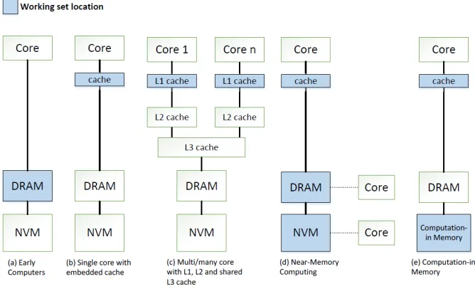
Figure 2.1: Architecture overview of traditional PIM paradigms based on the location of the working set of data. Figures (a), (b), and (c) show typical Von Neumann architectures with a separation of processing circuits and memory. Data is passed from DRAM or cache memory to be operated on by the processing core. The Near-Memory Computing paradigm is shown in (d), where processing cores are placed very close to the DRAM and Non-Volatile Memory. In doing so, the delay of transmitting data to a processing unit can be reduced due to the shorter travel distance. The Processing-in-Memory architecture, also called Computation in Memory, is shown in (e). Processing units are embedded directly within the DRAM memory, reducing delay by eliminating the need for costly data transfers. [6].
incurs minimal latency. Further development of HMC, however, will not be supported by
Micron. Other approaches include using specialized circuits within the RAM blocks [10]
or using novel Non-Volatile Memory devices such as Resistive RAM (ReRAM), which is
constructed using memristors, to perform logic within the memory cells [11]. Using these
advancements, small and efficient PIM architectures can be designed for a wide range
of applications. Typically, these architectures are designed to be application specific and
offer minimal flexibility. Some examples of application specific PIM architectures are a
Multiply-Accumulate engine [12], neural network engines [13, 14], and image recognition
CHAPTER 2. BACKGROUND
2.2
Matrix Multiplication
The Multiply-Accumulate (MAC) Operation is a powerful function that is used in a wide
range of applications. It is the primary operation when performing matrix multiplication,
which is used frequently by convolutional neural networks (CNNs). CNNs are very popular
in modern technology trends due to their ability to break down and classify data, commonly
for image recognition and other machine learning applications. The equation for a MAC
operation is given in Equation 2.1.
A←A+B×C (2.1)
In Equation 2.1, B and C are the primary operands to multiply together. The result
of the operation is then added to the accumulator, A. After repeated MAC operations,
the accumulator will contain the final summation of each multiplication product. In a
hardware implementation with a fixed bit length whereB andC have n bits, the size of
the accumulator must be at least 2n bits long to successfully store the result of one MAC
operation. To prevent overflow in repeated MAC operations, one extra bit is needed for
every two successive operations to store the carry out of the addition.
A large issue with the MAC operation, however, is its high memory access frequency.
During each MAC operation, theB andC values must be retrieved from memory. These
values are not guaranteed to be stored close to each other in memory, making efficient
caching difficult. This can cause a large memory access penalty by frequently retrieving
values from main memory, leading to a low computation to communication ratio and
degrading the overall performance. One potential solution to this problem is to use two
separate memories to hold B and C in order to maximize spatial locality of successive
operands.
Multiplication of two matrices can be performed using repeated MAC operations on
CHAPTER 2. BACKGROUND
is shown below where each element of the matrixCmxnis given by Equation 2.2.
a11 a12 . . . a1p
a21 a22 . . . a2p ..
. ... . .. ...
am1 am2 . . . amp ×
b11 b12 . . . b1n
b21 b22 . . . b2n ..
. ... . .. ...
bp1 bp2 . . . bpn =
c11 c12 . . . c1n
c21 c22 . . . c2n ..
. ... . .. ...
cm1 cm2 . . . cmn
cij =
p
X
k=0
aikbkj (2.2)
During each iteration of the summation in Equation 2.2, elements of theAmxpandBpxn
matrix are multiplied together and the product is accumulated for all iterations. Using
this, the element of the resulting matrix cij can be calculated through a series of MAC
operations. In addition, each element of the Cmxn matrix is independent from the other
elements and can therefore each element can be computed in parallel.
2.3
Networks-on-Chip
Advances in fabrication technology have allowed integrated circuit designs to be
exponent-ially larger and support extremely complex designs. Managing the flow of data across
these large, complicated designs has steered circuit designers towards the use of
Systems-on-Chips (SoCs) in order to ease the design. Systems-on-Chip design consists of many
independent modules being connected together, typically through a shared bus. This eases
the design process by allowing components to be reused between designs. Instead of
designing commonly used components from scratch, Intellectual Property (IP) can be
purch-ased or reused from previous designs. The design process then shifts to the integration and
connection of these parts rather than low level module design.
CHAPTER 2. BACKGROUND
with many components. Interconnect strategies such as shared buses cannot effectively
support a large number of components on the bus due to contention over the shared medium.
SoCs also face issues such as global synchronization due to the difficulties of creating a
high speed, robust clock across the chip [16]. In response to this, recent design trends have
shifted towards the Network-on-Chip (NoC) paradigm.
In a Network-on-Chip, the components are linked together through the use of switches
and routers, similar to traditional computer networks. This allows multiple independent
links to be used to pass data between components rather than a single shared medium.
Efficient design of the network topology connecting the components can allow them to
communicate with one another quickly and with a minimal number of hops between routers.
Topologies such as Small World Networks allow for a high scalability by minimizing the
typical distance between any two nodes in the network through the use of both short and
long distance links [17]. Designing for scalability allows new nodes to be added to or
removed from the network with minimal impact on the number of hops required to reach
any other node, which is ideal for networks with a large number of nodes.
2.4
Wireless Networks-on-Chip
Improvements in the fabrication process and technology node shrinks in continuation with
Moore’s Law have allowed for the production of increasingly complex circuits. Connecting
the components in these circuits becomes an issue, however, as metal interconnects are not
scaling in performance at the same rate as the transistors. The NoC paradigm helped to
alleviate this issue by offering a more efficient communication framework for components
on the chip, however its effectiveness is limited by the physical distance separating the
components. The performance of long metal wires is limited by the RC delay incurred
by the wires, which becomes more apparent as the technology node continues to shrink.
Unique solutions have been proposed to address this issue such as 3-dimensional integrated
CHAPTER 2. BACKGROUND
Wireless interconnects are designed to overcome the large RC delay of long metal
wires by using electromagnetic waves to send and receive data between modules. Metal
wires are still used for short routing, however the integrated wireless transceivers working
at 16Gb/s [17] allow data to be sent across long distances in significantly less time and
requires less power. Control of the shared wireless medium requires accessing a Multiple
Access Control (MAC) protocol to be implemented, such as Code Division Multiple Access
(CDMA), Time Division Multiple Access (TDMA), or Carrier-Sense Multiple
Access-(CSMA) [17].
Some drawbacks of using wireless interconnects include the overhead of the MAC
protocol, increased area due to the wireless transceiver circuits, and increased fabrication
difficulty. They make up for these drawbacks, however, by offering high speed data transfer
across large on-chip distances. In addition, multi-casting and broadcasting of data to
multiple wireless transceivers is inherently supported by the architecture as multiple
rec-eivers can read the same transmission simultaneously.
2.5
Supporting Work
Due to the manufacturing complexity of integrating dense logic and DRAM on the same
die, processing in memory was a relatively unexplored field for many years. A new rush of
PIM designs was recently enabled by Micron’s Hybrid Memory Cube (HMC) architecture
[8], which uses 3D stacked memory to enable logic and memory to be closely integrated.
HMC is constructed by stacking 4-8 dies of DRAM memory onto a base logic layer. All
of the layers in the stack are connected using Through-Silicon Vias (TSVs), which act as
high speed buses to transmit data between the layers. Many PIM architectures use HMC as
a basis for their designs due to the ability to integrate computational logic within the logic
layer of the package, which enables computations to be performed very close to memory.
Micron has since stopped their support of HMC. An alternative to HMC comes in the
CHAPTER 2. BACKGROUND
uses a 3D stack of DRAM dies connected by TSVs. Unlike HMC, however, HBM is
designed to connect directly to a CPU/GPU through a silicon interposer which offers high
speed communication between the components. Future PIM designs will likely be designed
around the use of HBM memory.
Typically, PIM architectures are designed to perform a single task such as
Multiply-Accumulate (MAC) operations [12], Convolutional Neural Network (CNN) operations
[14], or image processing [15]. Other PIM architectures have been designed for database
searches, data analysis, and graph processing [6]. These architectures are able to offer
a significant speedup over conventional computing for their designed tasks but lack the
flexibility to be used in other situations. In doing so, these designs limit their viability
outside of application specific hardware. In contrast to this, the proposed architecture will
be reconfigurable to allow for arbitrary functions to be implemented.
Currently, a matrix multiplication algorithm is envisioned using the proposed
archi-tecture. This will allow rapid computations for use in CNNs, which are used frequently
in artificial intelligence and image recognition applications. As a result, the proposed
architecture can be compared to both [12] and [14]. The architecture proposed in [12]
makes use of HMC to incorporate MAC processors near the data lines that access the
3D stacked memory. In each HMC-MAC instruction, a series of MAC operations are
performed using data supplied by the host processor and the memory. An HMC controller
is added to the host processor and is used to assemble the host supplied values for the MAC
operation as well as manage communications with the HMC module using one of 6 created
instructions. Similar to the proposed architecture, [12] is capable of performing multiple
repeated MAC instructions in parallel across the available memory. By constructing the
MAC unit close to the high bandwidth data line of the stacked DRAM, a high volume of
data can be processed quickly with minimal communication time.
Another comparable architecture is shown in [13], which is designed to perform CNN
CHAPTER 2. BACKGROUND
bandwidth data lines of the HMC module. The CLUs are designed to perform convolution
operations which form the basis of CNNs. The design makes use of a floating point
multiplier, floating point adder, and embedded SRAM to quickly apply filter values to a
dataset. The floating point operations are done using IEEE-754 double precision format
to maintain accuracy. An issue with this, however, is the large silicon area required to
implement it due to the complex circuitry required. This is an issue in PIM applications
where a small, low impact circuits are a priority.
Both [12] and [13] show significant improvement over conventional processing
archi-tectures due to their highly efficient specialized designs. The minimal data communication
time between the processing element and the memory allowed both architectures to obtain
effective processing rates that were far greater than a traditional processing and memory
structure. Where both architectures falter, however, is for general use cases. In applications
which do not directly conform to their intended domain, both architectures would offer
no performance improvements while still taking up valuable silicon area on the die. The
proposed architecture aims to improve upon this by allowing for full reconfigurability
of the operation to perform. Since any arbitrary function can be implemented using the
proposed architecture, any theoretical workload which requires frequent memory accesses
can instead be performed in the memory with significantly reduced communication latency.
Many modern PIM designs also focus on the use of Resistive Random Access Memory
(ReRAM) to perform arithmetic operations within the memory storage units themselves.
ReRAM is a type of non-volatile memory built using memristors, which store data using
programmable resistive states. Both a high and low resistive states can be stored into a
memristor by controlling the voltage difference across it. Binary values of ”0” and ”1” can
then be read as a function of the current through the memristor, where a high resistive states
equate to logic ”0” and low resistive states are logic ”1”. State-of-the-art PIM designs such
as [20], [21], and [22] use this ability to implement functions directly within the memory
CHAPTER 2. BACKGROUND
In [20], a ReRAM crossbar array is used to perform neural network operations using
the resistive states of the memory cells. Inputs are sent to the array as analog voltages
and the weights are represented as the resistive states. The current flowing through the
outputs is based on the resistances of the cells and determines the output value. This design
is capable of very fast and compact operations by using the memory cells as logic units,
however it requires a wide range of dedicated peripheral hardware to function. To perform
the neural network functions, the design requires digital-to-analog converters,
analog-to-digital converters, sigmoid units, and subtraction circuits [20]. This array of peripheral
circuitry tailored to perform neural network operations limits the overall flexibility of the
design as supporting other logic functions would require additional peripherals.
The designs proposed in [21] and [22] are similar to [20] in that they perform neural
network operations within the memory cell array. They differ, however, by implementing a
pipelined based approach where layers of the neural network can be processed in a parallel
manner. Both designs use pipeline stages to execute small portions of the layers at a time
and use the results in future pipeline stages. The design in [22] improves upon [21] by
avoiding pipeline bubbles and maintaining a constant series of operations through the
pipeline such that the efficiency is optimized. Similar to the issues described for [20],
these designs are highly specialized to perform neural network operations, reducing their
flexibility to be used for a wide range of tasks. Implementation of other functions would
Chapter 3
Processing-in-Memory Architecture
The center of the proposed architecture is the PIM Core which functions as the primary
logic unit. The PIM Core is capable of performing reconfigurable functions on two 4-bit
inputs to produce an 8-bit output. Nine PIM cores were then grouped together to form a
PIM Cluster to perform larger operations such as Multiply-Accumulate (MAC) using 8-bit
operands. An array of PIM Clusters can then be used to perform large scale operations
such as matrix multiplication in parallel.
3.1
PIM Core
The primary logic of the proposed architecture is the small, simple PIM Core which is
capable of performing arbitrary 4-bit operations. A primary objective of this architecture is
flexibility to support a wide range of potential applications. To achieve this, the PIM Core
functions similarly to a large LookUp Table (LUT) with the function to implement being
stored in memory. This allows the PIM Core to implement any arbitrary function based on
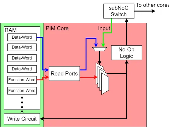
the data that is stored in memory. A block diagram of the PIM core is shown in Figure 3.1.
The LUT functionality is achieved using an 8-bit, 256-to-1 multiplexer. The 8-bit
multiplexer is required to support the multiplication of two 4-bit operands, which results in
an 8-bit result. The multiplexer has eight select lines which are used to determine the 8-bit
output given 256 8-bit options. The select lines are controlled by two 4-bit inputs which
CHAPTER 3. PROCESSING-IN-MEMORY ARCHITECTURE
Figure 3.1: High level block diagram of the proposed PIM Core. The PIM Core logic is shown within the red boundary.
The inputs to the multiplexer representing the function to implement are read directly
from the Random Access Memory (RAM) block and are referred to as function-words,
shown in Figure 3.1 as the red arrow. New functions can therefore be implemented on the
PIM Core by reading a new set offunction-wordsfrom the RAM block using the read port.
Many sets offunction-wordscan be stored in the memory to allow for rapid reconfiguration
of the PIM Core function to implement. This allows the PIM Core to implement addition,
subtraction, multiplication, or other Boolean functions dynamically by reading new values
from RAM, allowing the PIM Core to remain flexible to perform different tasks while still
being constructed using simple logic.
The two 4-bit inputs which are connected to the select lines of the multiplexer and
serve as the operators to the function are referred to asdata-words. These values can either
be obtained from RAM, or they can be given through a sub Network-on-Chip (subNoC)
switch which is attached to the PIM Core. Values obtained from the RAM block, shown
in Figure 3.1 using a blue arrow, can be used to process data stored in memory by a host
device. In contrast, values obtained from the subNoC switch, shown as a green arrow, can
CHAPTER 3. PROCESSING-IN-MEMORY ARCHITECTURE
to transmit data between locally adjacent cores contained within the same PIM Cluster.
The subNoC connections are discussed further in Section 3.3. These connections between
cores allows larger functions to be implemented using multiple PIM Cores, as results from
other operations can be used as inputs to the PIM Core.
The included No-Op logic block will be used reduce total communication time for
sparse data applications. When the result of a PIM Core operation is equal to zero, the
No-Op detection block will prevent the data from being sent out of the core. A zero value
will then be inferred by the lack of data from the core and no additional time or energy will
be used to transmit the data.
3.2
Multiply-Accumulate Using PIM Cores
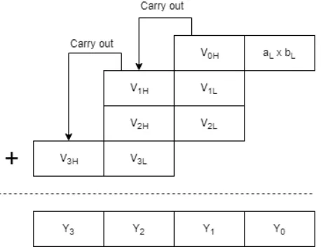
To complete matrix multiplication operations, an 8-bit Multiply-Accumulate (MAC)
funct-ion was implemented using a PIM Cores, resulting in a 16-bit value. To achieve this,
the 8-bit MAC instruction was decomposed into a series of 4-bit operations which can be
performed by the PIM Cores. The Multiply-Accumulate (MAC) instruction contains two
primary operations, an 8-bit multiplication and a 16-bit addition. The multiplication can be
broken down into a series of 4-bit multiplications resulting in 8-bit partial products, which
can then be added together to form the final result. The partial products Vx are defined
as follows, where the subscripts H and Lrepresent the upper and lower four bits of the
operand respectively:
1. V0 =aL×bL
2. V1 =aL×bH
3. V2 =aH ×bL
4. V3 =aH ×bH
After obtaining the partial products Vx through multiplication, the final product Y
CHAPTER 3. PROCESSING-IN-MEMORY ARCHITECTURE
multiplication result of two 8-bit numbers will always be contained within 16-bits, therefore
[image:26.612.212.441.126.302.2]there is no need for overflow protection.
Figure 3.2: Decomposition of 8-bit multiplication into a series of 4-bit multiplications and additions.
The 16-bit addition operation can be decomposed into a series of 4-bit additions in
a similar manner. Ripple-carry addition is used to compute the final 16-bit result. This
process is shown in Figure 3.3 in the context of the MAC operation, where the 16-bit
multiplication resultY is added to the 16-bit accumulatorAand the result is stored intoA.
Figure 3.3:Decomposition of 16-bit addition into a series of 4-bit additions.
The size of the accumulator can be increased in order to account for additional overflow
which is generated through repeated additions. In this work, the accumulator size was
[image:26.612.212.441.464.590.2]CHAPTER 3. PROCESSING-IN-MEMORY ARCHITECTURE
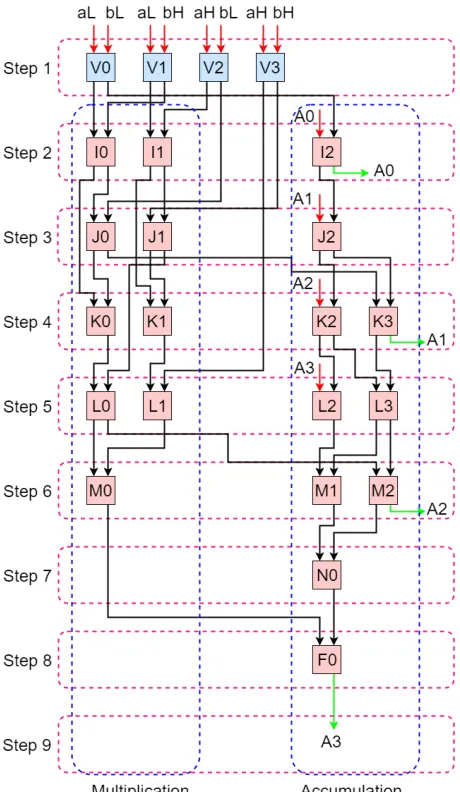
The multiplication and addition algorithms can then be translated to be performed using
PIM Cores. A sequential model for performing the MAC operation was created where
the output of each PIM core is sent directly to the input of another core. A diagram of
the sequential model PIM MAC operation is shown in Figure 3.4, where each PIM Core
is given a unique identifying label. Each core within the diagram represents a single
4-bit operation of the decomposed multiplication and addition operations. The left side of
the diagram represents the operations required to perform the addition of partial products,
CHAPTER 3. PROCESSING-IN-MEMORY ARCHITECTURE
Figure 3.4: Sequential model of 8-bit MAC operation. In the figure, blue boxes represent 4-bit multiplication and red boxes represent 4-bit addition. The arrows coming out of each box represent the upper and lower 4-bit results of the core’s operation. The upper four bits are denoted by the left arrow, while the right arrow represents the lower four bits. The red arrows designate inputs to the system in the form of the inputsaandbas well as the accumulatorA. The final accumulator results are denoted with a green arrow.
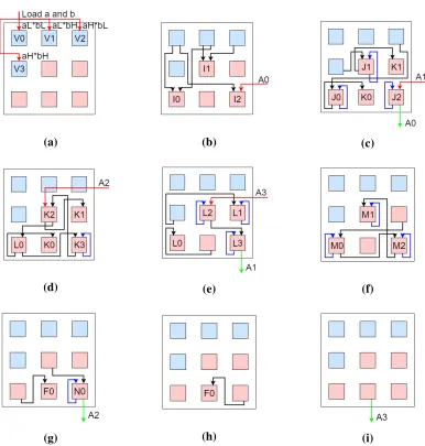
The sequential model is designed such that each PIM Core will be utilized once during
the MAC instruction. This configuration simplifies the flow of data, however it uses
signif-icantly more resources than is necessary to complete the instruction. In the sequential
model, 23 PIM Cores are required to complete the operation. By reusing cores to compute
CHAPTER 3. PROCESSING-IN-MEMORY ARCHITECTURE
designated as the compact model, uses data destinations that change based on which portion
of the MAC operation is being computed.
The complete set of steps required to execute the compact model are shown in Figure
3.5. During each step in the figure, the cores are labeled to match the corresponding
operation from the sequential model in Figure 3.4. Similar to the sequential model, black
arrows show communications between the cores, the red arrows designate inputs to the
system, and the green arrows denote completed accumulator outputs. In Figure 3.5, the blue
arrows represent the core internally holding a result from its operation for use in the next
calculation, reducing the amount of data that needs to be transmitted. This MAC operation
can be repeated multiple times using a shared accumulator value in order to execute dot
product operations, which will be used to perform matrix multiplication.
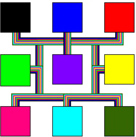
3.3
PIM Cluster
In order to facilitate larger operations such as the proposed 8-bit MAC scheme, groups of
nine PIM Cores connected together to form a PIM Cluster. The nine PIM Cores within
a cluster are connected using the sub Network-on-Chip (subNoC), an all-to-all network
such that any core can directly send data to and receive data from any other core within
the cluster. This interconnection fabric is shown in Figure 3.6. Communication between
the PIM Cores is implemented through the transmission of single 32-bit packets, or Flow
Control Units (flits).
This interconnection fabric was chosen due to the low data output size, close physical
proximity, and high speed requirements of the PIM Cores. By directly linking cores
together, the high overhead of traditional Network-on-Chip (NoC) architectures such as
ring and mesh networks can be eliminated. The overhead required in these networks
includes area and power used by the switches and routers in addition to increased latency
due to multi-hop routing. Using the All-to-All network, delay penalties are limited to the
CHAPTER 3. PROCESSING-IN-MEMORY ARCHITECTURE
(a) (b) (c)
(d) (e) (f)
[image:30.612.134.520.179.584.2](g) (h) (i)
CHAPTER 3. PROCESSING-IN-MEMORY ARCHITECTURE
Figure 3.6:All-to-All Network connecting the nine PIM Cores within a PIM Cluster. Each colored wire represents a bidirectional communication path between two PIM Cores.
The All-to-All network is not scalable for larger sized networks due to the large number
of connections needed. In this architecture, however, where the size of the network is
limited to nine nodes, it is sufficient. If the number of PIM Cores contained in a cluster were
to be increased, the network topology connecting them would likely need to be reevaluated
and modified to support the larger number of nodes. For larger cluster sizes, a mesh
network topology would be more beneficial due to the reduced number of connections
needed, however this would require additional area, power, and logic to support routing
data between the cores.
A key benefit of the All-to-All network is its flexibility to enable arbitrary communication
between any two PIM Cores rather than relying on fixed paths. In this section, an 8-bit
MAC operation was implemented using PIM Core logic, however other functions can be
implemented by changing the function-wordsof each core and defining different routing
behavior. By doing this, other large functions such as 32-bit addition or multiplication can
be achieved using the PIM Cluster.
CHAPTER 3. PROCESSING-IN-MEMORY ARCHITECTURE
the use of routing logic located in the center of the cluster. This router will be integrated
into a 2-D mesh NoC architecture to facilitate communication with other PIM Clusters
and Memory Controllers (MCs), forming a two-tiered hierarchical mesh. This router can
be implemented using traditional wired interconnects or using high performance wireless
interconnects. Due to the 16-bit results generated by PIM Cluster operations, the
commun-ication can occur through single 32-bit flit transmissions using the same flit structure as the
subNoC. This enables larger scale functions to be implemented using the PIM architecture,
such as Matrix Multiplication.
3.4
Matrix Multiplication Using PIM Clusters
A scheme for performing matrix multiplication operations using the outlined PIM
architect-ure is proposed. This PIM architectarchitect-ure is suited for computing matrix multiplication as PIM
Clusters can compute an element in the result matrix through repeated MAC operations. By
using a 2D array of PIM Clusters, each element of the result matrix can be calculated in
parallel.
In order to perform the matrix multiplication operations, the relevant row and column
data from the input matrices must be loaded into each cluster. Data inputs to the PIM
clusters is handled through the use of multicasting, which allows data to be sent to multiple
destinations within the 2D array of PIM Clusters. As a result, rows/columns of data from
the input matrices can be sent to all clusters which require the data at the same time.
Multicasting data for matrix multiplication of two matrices A and B to produce a 3x3
matrixC is exemplified in Figure 3.7.
After a PIM Cluster receives the input data, it can begin performing MAC operations.
As shown in Equation 2.2, the number of MAC operations to perform in each cluster is
equal to the size of the shared dimension of the two input matrices,P. Using the input data
distribution method shown in Figure 3.7, the time when a PIM Cluster finishes allP MAC
CHAPTER 3. PROCESSING-IN-MEMORY ARCHITECTURE
(a) (b)
[image:33.612.129.524.73.475.2](c) (d)
Figure 3.7:Multicasting scheme to transmit data for matrix multiplication. (a) First row of column Ais sent to the first row of clusters. (b) First column ofBis sent to the first column of clusters. (c) Second row ofAis sent to the second row of clusters. (d) Second column ofBis sent to the second column of clusters. The process is continued until all rows and columns from the input matrices are sent to the clusters.
which receive both sets of input data can begin computation while the rest of the inputs are
being transmitted. After each cluster finishes its computations and produces a final result,
Chapter 4
Analytical Modeling of PIM Cluster
4.1
PIM Cluster Area
Each PIM Cluster contains nine PIM Cores which are arranged as a 3x3 array. In this
analysis, the cores are assumed to be located directly next to each other in a uniform
grid such that no gaps exist between the cores. In addition, each cluster is assumed to be
surrounded by a block of RAM which can be used to hold localdata-wordsand
function-words. A memory access port is assumed to be located on the outer boundary of the PIM
[image:34.612.224.424.448.648.2]cores. A diagram of the PIM Cluster is shown in Figure 4.1.
CHAPTER 4. ANALYTICAL MODELING OF PIM CLUSTER
interconnects used to transmit data between the cores is assumed to originate at the center
of the core. To ensure the validity of the design, it must be possible to retrieve data from
any other core or the memory and perform a computation within a single clock cycle. The
worst case core-to-core communication path occurs when data is sent across the diagonal
of the 3x3 array, as shown by the red line in Figure 4.1. This Manhattan distance can be
obtained in terms of the side length of a PIM Core,LP IM. The data must travel through the
lengths of three PIM Cores as well as two times the distance from the center of the core to
a perpendicular edge. The total length is therefore equal to4LP IM.
The total delay incurred by this distance can then be obtained using the Elmore Delay
model shown in Equation 4.1 in conjunction with a known interconnect RC delay
measure-ment for a given process node. The known interconnect RC delay is given in ps/mm, which
can be expressed as a reference delayTref divided by a reference distanceLref. By keeping
the values of randcconstant and using the reference RC delay, the Elmore Delay model
can then be rearranged to calculate the interconnect delay for a given interconnect length,
Tintas shown in Equation 4.2.
D= 0.4rcL2 (4.1)
Tint=Tref ×
Lint Lref
2
(4.2)
The same procedure is repeated to obtain the delay of the longest core-to-memory path,
which is shown by the blue line in Figure 4.1. In this longest path, the data must travel
through the length of four PIM Cores in addition to two times the distance from the center
of the core to the perpendicular edge. The total distance is therefore equal to5LP IM. The
CHAPTER 4. ANALYTICAL MODELING OF PIM CLUSTER
4.2
PIM Cluster MAC Energy
The total energy required to perform a MAC operation using a PIM Cluster is equal to the
total energy used by the PIM Cores and wired interconnects during each of the nine steps
of the MAC operation. The total power of a single PIM Core,Pcorecan be obtained through
static power analysis using circuit analysis tools. The energy used by the core,Ecore, can
then be obtained by multiplying the core power by the delay of the PIM Core. The delay
of the PIM Core can also be obtained using circuit analysis tools. During operation, each
of the nine PIM Cores is assumed to be fully powered on, therefore the total energy used
by the cores is equal to9Ecore.
The total power of the interconnects was calculated by measuring the distance traveled
by data during each step of the MAC operation. The distance of each data communication
was obtained by using the Manhattan distance between the centers of the source and
destination PIM Cores. This distance, Lintij, was determined for every data transmission
during each of the nine steps of the MAC operation, wherei is the numbered step of the
operation and j is the number of the transmission during step i. Using the capacitance
per unit length for a given technology node, cint, the transmission energy of sending the
32-bit packet can be obtained using Equation 4.3, whereα is the activity factor andV is
the supply voltage.
Eintij = 32×α×(cint×Lintij)×V
2 (4.3)
The total energy used by the interconnects during a MAC operation can then obtained
through a summation of the energy used by each of the interconnects, as shown in Equation
4.4, wherenis the number of data transmissions present during stepiof the MAC operation.
Eint T otal =
9
X
i=1
n X
j=1
CHAPTER 4. ANALYTICAL MODELING OF PIM CLUSTER
The total energy used during an entire MAC operation using the PIM Cluster can then
be expressed as the sum of the energy used by nine PIM Cores for nine steps and the
interconnect energy, as shown in Equation 4.5.
EM AC = 9×9Ecore+Eint T otal (4.5)
The static power of the PIM Cores and interconnects are not considered in any of the
energy models. Instead, the models are entirely based on the dynamic energy required to
perform the operations. This allows the models to more closely reflect the energy used by
the algorithms themselves rather than intrinsic device characteristics. In addition, the static
and dynamic energy required by the memory is not included because it is dependent on
the type of memory used and the size of the memory, which have not been defined in this
architecture.
4.3
PIM Cluster MAC Timing
The time required to complete a MAC operation within a cluster,TM AC, can be expressed
as the sum of the core processing time,TP IM, and the delays caused by the interconnects,
as shown in Equation 4.6. The PIM Core processing time can be obtained using static
timing analysis with circuit analysis software.
TM AC =
9
X
i=1
TP IM +Tinti (4.6)
The delay caused by the wired interconnects during a given step i, Tinti, represents
the longest delay caused by transmission lines during each of the nine steps of the MAC
operation. The delay changes during each of the steps of the MAC operation due to the
different data communication patterns present during each step. The interconnect delay of
each step can be obtained by finding the longest data communication distance. The longest
CHAPTER 4. ANALYTICAL MODELING OF PIM CLUSTER
Chapter 5
Timing Analysis Models
5.1
Matrix Multiplication Using Wired Interconnects
Matrix multiplication is achieved by performing repeated MAC operations in each of the
PIM Clusters. Each PIM Cluster computes a final element of the resulting matrix in
parallel. This operation can be broken into three primary steps: sending input matrix data
to the PIM Clusters, performing MAC operations using the data, and transmitting the final
result to a Memory Controller (MC) to store it into memory. The time to send the input data
and receive the final results are dependent on the interconnect architecture used to connect
the PIM Clusters and the MC while the time to perform the MAC operations is invariant.
In this section, the timing and power of completing a matrix multiplication operation using
an array of PIM Clusters connected with wired interconnects is proposed.
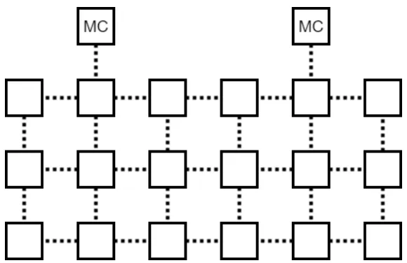
The PIM Clusters are assumed to be arranged as a 2D grid and connected using a 2-D
mesh network. The clusters are assumed to be laid out such that distance incurred by hops
between has an RC delay of 1ns. In addition, the routers used to control the flow of data
communications is assumed to cause a delay of 1ns. The combination of these two delays
is denoted asThop. The MCs are assumed to be located along one edge of the array of PIM
Clusters and are connected to the mesh network through an adjacent PIM Cluster. This link
between the MCs and the PIM Clusters also has an RC delay of Thop. This configuration
is exemplified in Figure 5.1. The proposed model assumes a variable number of MCs can
CHAPTER 5. TIMING ANALYSIS MODELS
Figure 5.1: Example configuration of PIM Cluster array and 2-D mesh network. Two Memory Controllers are evenly distributed over the six columns of the array. The dashed lines represent the interconnects of the mesh network.
MC will be responsible for distributing data to the columns closest to it, which allows for
increased parallelism. The number of columns controlled by each MC is assumed to be
an equal portion of the maximum number of clusters. Cases with 1, 4, and 8 MCs are
examined.
To perform timing analysis using the circuit setup outlined in Figure 5.1, a set of
variables describing the setup of the PIM Cluster array was used. The array of clusters
is assumed to have M rows and N columns. The size of the shared dimension between
the two input matrices, which determines the number of MAC operations to perform, isP.
The following variables are then used for analysis, where nmc is the number of memory
controllers in the system:
1. ctotal = l N
nmc m
2. cmc =
l N
2×nmc m
3. clef t =cmc−1
CHAPTER 5. TIMING ANALYSIS MODELS
The variablectotalis the largest number of columns which is assigned to any MC in the
system. For configurations in which the memory controllers cannot be evenly distributed,
some MCs will be tasked with providing data to more clusters than others. The next
variable, cmc, represents the column index of the MC within its assigned columns. The
value of cmc is 1-indexed such that a value of ’1’ depicts that the memory controller is
located in the leftmost column. Finally, theclef tandcright variables denote the number of
columns to the left and right of the MC, respectively. In unequally distributed systems, the
number of columns on the left and right will be different. Using these variables, the timing
and power of the system can be quantified.
5.1.1 Sending Input Data
Data from the input matrices can be sent to the clusters in a row-wise or column-wise
fashion, which will be referred to asrow-castingandcolumn-casting, respectively. These
transmission schemes allow an entire row/column of PIM Clusters to obtain the same input
data while minimizing the total data communication time. The scheme used to perform
[image:41.612.182.469.456.644.2]row-casting is shown in Figure 5.2.
Figure 5.2: Example of sending data to PIM Clusters located in row 3 of the 2-D array. The two MCs work in conjunction to cast data across the row.
CHAPTER 5. TIMING ANALYSIS MODELS
row-cast to a given row,i, was derived. To reach the given row,ihops are needed to travel
down the column containing the MC. Then, the data branches and transmits to the left and
right columns simultaneously. The number of hops required to fully branch to the left and
right columns is determined by the maximum ofclef t andcright. When performing matrix
multiplication, an entire row/column of data with P elements is needed, therefore a total
of P elements are required to be transmitted to all clusters in the row. These values can
be transmitted in a lock-step fashion such that the next value will be one hop behind the
current transmission. The total time to row-cast to a given rowiis the sum of these times,
as shown in Equation 5.1. Since the row-casting done under each MC is done in parallel,
the total execution time is equal to the worst case of any given grouping of columns under
an MC.
Trow(i) = (i+max(clef t, cright) + (P −1))×Thop (5.1)
During the course of a matrix multiplication, data is cast to every row in the PIM Cluster
array. The total time to send all rows of data can be expressed as the sum to row-cast the
data to every row of clusters, as shown in Equation 5.2.
Trow total = M X
i=1
Trow(i) (5.2)
Column-casting can be used to send the data to all clusters in the same column of the
PIM array. The scheme used to perform column-casting is shown in Figure 5.3. Data is first
directed to the required column, then the data is propagated down the column such that it
reaches every cluster in the column. The number of hops required to reach a given column
j is equal to the number of columns betweenjand the closest MC. Similar to row-casting,
P elements are required to be transmitted in lock-step fashion after the first data element.
If the value ofj is assumed to be a local index between 1 andctotal, then the time required
CHAPTER 5. TIMING ANALYSIS MODELS
Figure 5.3: Example of sending data to PIM Clusters located in columns 1 and 4 of the 2-D array. The two MCs work in conjunction to cast two columns of data simultaneously.
Tcol(j) = (|cmc−j|+M + (P −1))×Thop (5.3)
During a matrix multiplication operation, values will be column-cast to every column
of the PIM cluster array. Each MC can perform column-cast operations on its assigned
columns in parallel, therefore the total time to column-cast all the data is limited by the
grouping with the most columns. The total time to column-cast the data can be separated
into two primary stages; time to hop to the correct column and time to transmit the data
down the correct column. The total number of hops required to reach every column across
all required column-casts,nhopsis expressed in Equation 5.4.
nhops= clef t
X
k=1
k+ cright
X
k=1
k (5.4)
The number of hops required to transmit data down a column is equal to the number
of rows in the column. Since each column within the MC grouping requires a column-cast
to obtain data, this number of hops must be repeatedctotal times. This, combined with the
CHAPTER 5. TIMING ANALYSIS MODELS
in Equation 5.5.
Tcol total=ctotal×(M + (P −1))×Thop+nhops×Thop (5.5)
5.1.2 PIM Computation
The number of MAC operations to perform on the input data is given by the size of the
shared dimension between the two input matrices,P. Each cluster in the PIM Cluster array
is required to performP MAC operations to produce a final element in the result matrix.
Each cluster’s computations can be performed in parallel due to data independence. As a
result, the total time required to perform all computations,Tcompute, is equal to the time to
performP MAC operations, as expressed in Equation 5.6.
Tcompute=P ×TM AC (5.6)
5.1.3 Data Retrieval
After each cluster completes its computations, it produces a single value in the result matrix
which it must transmit to the memory controller to be stored into memory. This can be
performed in a lock-step fashion where results are funneled to the memory controller as
adjacent clusters send their results. The result of this is a result reaching the MC after every
hop. Within each MC’s grouping exist at mostM rows andctotalcolumns of PIM Clusters.
Therefore the maximum number of results to transmit is the equal to the product ofM and
ctotal. Using this, the maximum total time to retrieve the data,TRmax is given in Equation
5.7.
TRmax =M×ctotal×Thop (5.7)
Due to the included No-Op logic where results with a value of zero are not transmitted,
CHAPTER 5. TIMING ANALYSIS MODELS
β. The value ofβexpresses the number of non-zero elements in the final result matrix and
their proximity to the MC. No formal function forβ is proposed, as it is outside the scope
of this investigation. In a worst case fully dense matrix with all elements of non-zero value,
β will have a maximum value of ’1’. A best case fully sparse matrix with all zero results
will have aβvalue of zero. Sparsity conditions between the best and worst cases will have
a value such that 0 < β < 1. The total time to retrieve the data from the clusters with
sparsity is expressed in Equation 5.8.
TRsparse(β) =β×TRmax (5.8)
5.1.4 Final Timing Model
Due to the parallel nature of the cluster operations, asymmetric data distribution scheme,
and fast computation time, the computation time of the MAC operations can be masked by
the data transmission times. The first PIM Cluster can begin computations after the first
row and column are multicast. During this computation time, input data will continue to be
transmitted to the clusters. This trend continues until all input data has been transmitted.
Once all input data has been transmitted, the results from the finished PIM Clusters can
begin being sent to the MCs. After all results are retrieved from the PIM Clusters, the
matrix multiplication operation is completed. A timing diagram outlining the steps of the
matrix multiplication operation is shown in Figure 5.4.
An equation for the total execution time is given in Equation 5.9, which accounts for
the masked execution time.
CHAPTER 5. TIMING ANALYSIS MODELS
Figure 5.4:Timing diagram of a matrix multiplication operation using wired mesh network.
5.2
Matrix Multiplication Using Wireless Interconnects
The proposed PIM architecture can also be implemented using a wireless interconnection
fabric. In this setup, the wired switch and router present in each cluster are replaced with
a wireless transceiver operating at 60GHz, based on the architecture proposed in [23]
and [24]. The throughput of the wireless network is given to be 16Gb/s. The wireless
transceiver is also used to facilitate communication with the memory controller. The use of
wireless interconnects allows a minimal transmission delay and simultaneous multicasting
and broadcasting to any clusters in the network. As a result, row-casting and
column-casting can be achieved without the need to transmit data using multiple hops. Similar to
the wired interconnect model, the total execution time of a matrix multiplication operation
can be broken into three primary stages: transmission of input data, computations using
PIM Clusters, and receiving final results. The computation time of the PIM clusters is
CHAPTER 5. TIMING ANALYSIS MODELS
5.2.1 Sending Input Data
Similar to the wired interconnect model, rows and columns of input data can be multicast
to multiple clusters in the PIM array. Unlike the wired, model, however, one MC is
responsible for wirelessly sending the data, which eliminates the parallelism gained by
using multiple MCs. The loss of parallelism is made up for by the rapid multicasting
which is possible using wireless interconnects. Input data can be sent into the array of PIM
Clusters using the same scheme as outlined in Figure 3.7. When a row-cast or column-cast
is made, all clusters within the destination row/column receive the data at the same time.
The time to perform a row-cast or column-cast is therefore equivalent to the time required
to transmit a series of 32-bit flits containing theP elements of the input row/column using
the wireless interconnects. The equation for calculating the time required to multicastP
elements using wireless interconnects,TM/C, is shown in Equation 5.10.
TM/C =P ×
32bits
16Gb/s (5.10)
To perform a matrix multiplication operation, each of the M rows andN columns of
input data must be sent to the clusters. Each of these transmissions requires a multicast
to send data to a given row/cluster, which requires TM/C time to perform. Using this, the
equation for the total time required to send input data,Tin, is shown in Equation 5.11.
Tin = (M +N)×TM/C (5.11)
5.2.2 Data Retrieval
Once a PIM Cluster has completed all of its MAC operations, it can transmit its final result
to the MC using the wireless transceiver. The cluster must wait for the wireless medium
to be available first, however, meaning that sending results cannot occur at the same time
CHAPTER 5. TIMING ANALYSIS MODELS
one at a time to the MC using 32-bit flits. In a fully dense matrix with all non-zero results,
each of theM×N elements must be sent to the MC, one at a time. In a sparse matrix with
S non-zero elements, onlySresults must be sent to the MC where0 <=S <=M ×N.
Therefore the time to send all result data to the MC can be expressed as shown in Equation
5.12.
Tresults(S) =S× 32bits
16Gb/s (5.12)
5.2.3 Final Timing Model
The total time to complete a matrix multiplication operation using wireless interconnects is
equal to the sum of the time to send data inputs, perform computations, and gather the final
results. As in the wired interconnect model presented in Section 5.1.4, the computation
time of the PIM Clusters can be masked by the data transmissions. This is exemplified in
[image:48.612.112.539.411.618.2]the timing diagram shown in Equation 5.5, which shows the timing of a fully dense matrix.
Figure 5.5:Timing diagram of a matrix multiplication operation using wireless interconnects.
For sparse matrices, the computation time will be masked only if the time to send the
CHAPTER 5. TIMING ANALYSIS MODELS
can complete. The final timing equation for the wireless interconnect model is given in
Equation 5.13.
Chapter 6
Energy Analysis Models
Like the timing model, the energy used to perform a matrix multiplication operation can
be divided into three primary sections: sending input data to the clusters, performing the
MAC operations within each cluster, and sending the results to a memory controller.
6.1
Matrix Multiplication Using Wired Interconnects
In the wired interconnect model, each of the PIM Clusters and MCs are connected in a 2-D
mesh network using switches and routers in each node. The distance between each node
is assumed to take 1ns to traverse. Using this delay and a modified version of Equation
4.2, the physical distance can be estimated as shown in Equation 6.1. Using the estimated
distance and known parasitic capacitance per unit length for a given technology node,cint,
the energy to traverse the distance, Ehop int, can be obtained using Equation 4.3. Each
router was assumed to use some amount of energy,Erouter, during its use. The total energy
per hop,Ehop, is therefore the sum ofEhop intandErouter.
Lhop=Lref × s
1ns Tref
CHAPTER 6. ENERGY ANALYSIS MODELS
6.1.1 Sending Input Data
Row-casting and column-casting are used to distribute data from the MCs to the desired
row or column in the array of PIM Clusters. The total energy used during each of these
operations is equal to the number of hops required for all the data to reach its final
destinat-ions multiplied by the energy per hop. To send P elements of data to row i of the array
using the scheme outlined in Figure 5.2, the data must travelihops to reach the correct row.
Then,ctotal−1hops are required to propagate the data throughout the row. This process is
repeated for each of theP data packets sent. The power used to row-cast to a given rowi
is expressed in Equation 6.2.
Erow(i) = (ctotal+i−1)×P ×Ehop (6.2)
During a column-cast, data must travel laterally from the column containing the MC to
the correct column, then travel down theM rows of the column. This data flow is repeated
for each of theP packets to send. The energy to perform a column cast to a given column
j can therefore be expressed as shown in Equation 6.3.
Ecol(j) = (|cmc−j|+M)×P ×Ehop (6.3)
The total amount of energy used to transmit all input data is equal to the energy required
to perform all row-cast and column-cast operations. In this process,M row-casts andctotal
column-casts are required for each MC. The total energy to send all input data is expressed
in Equation 6.4.
Einput = ( M X
i=1
Erow(i) + ctotal
X
j=1
CHAPTER 6. ENERGY ANALYSIS MODELS
6.1.2 PIM Computation
Each PIM Cluster in theM xN array must performP MAC operations during its
comput-ations. Each of these MAC operations requires EM AC energy to perform as derived in
Equation 4.5, which includes the energy of the PIM Cores and the subNoC interconnects.
The total energy used during the PIM Clusters during computations is expressed in Equation
6.5.
Ecompute =M ×N×P ×EM AC (6.5)
6.1.3 Data Retrieval
Data retrieval from the PIM Clusters in the wired mesh network functions such that the
results are funneled one at a time to the MC. The flow of data from the PIM Clusters to the
[image:52.612.233.412.398.573.2]MC follows a tree-like structure as shown in Figure 6.1.
Figure 6.1: Example of retrieving results from a 3x4 array of PIM Clusters using wired interconnects. Data is passed to the MC in a lock-step fashion. The numbers next to each interconnect represent the number of packets sent through the link during the data retrieval process.
The energy used during the data retrieval process can be calculated by counting the total
number of hops performed by each link to move all data to the MC. The number of times
CHAPTER 6. ENERGY ANALYSIS MODELS
Clusters in the rows below it. As shown in Figure 6.1, the vertical link connecting row 3
to row 2 is used 4 times because the 4 elements contained in row 4 must send their data
through the link. Similarly, the vertical link connecting row 2 and row 1 is used 8 times
because all the data contained in rows 2 and 3 must pass through the link. The total number
of times the horizontal links are used in each row is equal tonhops. In a dense matrix, the
total energy used can be obtained by multiplying the total number of hops by the energy
required per hop. For sparse matrices, however, where the number of non-zero results is
less than the number of PIM Clusters, the total energy usage depends on the number of
results and their location in the array. This sparsity characteristic is described through the
parameterβ. The total energy usage required to retrieve data from the array of PIM Clusters
is shown in Equation 6.6.
Eresults(β) = β×( M X
i=1
(ctotal×i+nhops))×Ehop (6.6)
6.1.4 Total energy
The total energy required to complete a matrix operation using the array of PIM Clusters
with wired interconnects is equal to the sum of the energy used to send the input data,
perform the MAC computations, and send the final results to the MCs. Of these values,
only the energy used to send final results is affected by the sparsity of the matrix. The total
energy is therefore expressed as shown in Equation 6.7.
CHAPTER 6. ENERGY ANALYSIS MODELS
6.2
Matrix Multiplication Using Wireless Interconnects
6.2.1 Sending Input Data
Input data is sent to the array of PIM Clusters through the use of wireless
![Figure 1.1: Growing performance gap of processors and DRAM memory compared to technologyin 1980 [2].](https://thumb-us.123doks.com/thumbv2/123dok_us/24876.1926/12.612.154.495.70.262/figure-growing-performance-processors-dram-memory-compared-technologyin.webp)