City, University of London Institutional Repository
Citation:
Zhang, H., Zhou, L., Xu, J., Wang, N., Hu, H., Lu, L., Rahman, B. M. ORCID: 0000-0001-6384-0961 and Chen, J. (2019). Nonvolatile waveguide transmission tuning with electrically-driven ultra-small GST phase-change material. Science Bulletin, 64(11), pp. 782-789. doi: 10.1016/j.scib.2019.04.035This is the accepted version of the paper.
This version of the publication may differ from the final published
version.
Permanent repository link:
http://openaccess.city.ac.uk/id/eprint/22618/Link to published version:
http://dx.doi.org/10.1016/j.scib.2019.04.035Copyright and reuse: City Research Online aims to make research
outputs of City, University of London available to a wider audience.
Copyright and Moral Rights remain with the author(s) and/or copyright
holders. URLs from City Research Online may be freely distributed and
linked to.
City Research Online: http://openaccess.city.ac.uk/ [email protected]
1
Nonvolatile waveguide transmission tuning
with electrically-driven ultra-small GST
phase-change material
Hanyu Zhang1, Linjie Zhou1*, Jian Xu1, Ningning Wang1, Hao Hu1, Liangjun Lu1, B. M. A.
Rahman2, and Jianping Chen1
1State Key Laboratory of Advanced Optical Communication Systems and Networks,
Shanghai Key Lab of Navigation and Location Services, Shanghai Institute for Advanced
Communication and Data Science, Department of Electronic Engineering, Shanghai Jiao
Tong University, Shanghai 200240, China
2 Department of Electrical and Electronic Engineering, City, University of London, London
EC 1V 0HB, U.K.
*Corresponding author: [email protected]
Abstract:
Low-power reconfigurable optical circuits are highly demanded to satisfy a variety of different
applications. Conventional electro-optic and thermo-optic refractive index tuning methods in
silicon photonics are not suitable for reconfiguration of optical circuits due to their high static
power consumption and volatility. We propose and demonstrate a nonvolatile tuning method by
utilizing the reversible phase change property of GST integrated on top of the silicon waveguide.
The phase change is enabled by applying electrical pulses to the m-sized GST active region in a sandwich structure. The experimental results show that the optical transmission of the
silicon waveguide can be tuned by controlling the phase state of GST.
Keywords
Integrated optics; Optical storage materials; Integrated optics materials; Integrated optics
devices.
Introduction
Photonic integration is a development trend for optical systems that are widely used in various
optical interconnection and signal processing systems [1-3]. Similar to the application-specific
integrated circuits (ASICs), a photonic integrated circuit can also be designed to satisfy a
2
configuration [4, 5]. Although the performance can be well optimized after multiple rounds of
design and fabrication iterations, the lack of versatility makes it impossible to become a general
low-cost solution to various price-sensitive applications. Therefore, programmable optical
circuits are in high demand for general purposes, where different functions can be provided by
simply resetting several key components [6].
Waveguide refractive index (RI) tuning is the basis for actively tunable devices. In silicon
photonics, thermo-optic (TO) and electro-optic (EO) effects are routinely used for RI tuning,
but they are both volatile and require a continuous power supply to maintain the states. This
leads to large static power consumption, especially for reconfigurable optical circuits, like
optical circuit switches [7] and optical signal processors [8, 9] when the optical paths are not
frequently changed.
One solution for nonvolatile RI tuning is to integrate phase change material (PCM) with
silicon[10, 11]. The PCM has a dramatic change in the optical property after phase transition
between amorphous and crystalline states [12]. It is possible to obtain a large RI change of n >1.
Moreover, because of the stable phases, the tuned RI can be kept for a long time without power
consumption. This property makes it quite attractive for reconfigurable optical circuits.
Ge2Sb2Te5(GST) is a classical chalcogenide alloy in which the phase change can be actuated
either by thermal, optical or electrical stimulations potentially with an ultrahigh speed [13-17].
In recent years, there has been increased interest in GST for photonic devices. A lot of
exciting works have been done in photonic devices for applications targeted for neuromorphic
computing, multi-level storage, display, optical switches [18-20], and photonic in-memory
computing[21-25]. The optical switch can be based on a multimode interferometer (MMI) loaded
with GST and the phase change is enabled by light pulse irradiation from an out-of-plane laser
[18]. However, it is quite challenging to apply this method to a large-scale photonic integrated
circuit. An integrated all-photonic non-volatile multi-level memory has been demonstrated [24].
The phase change is induced by pump pulses from an in-plane waveguide. This method
improves the integration capability, suitable for all-optical signal processing.
In this work, we investigate nonvolatile optical transmission adjustment in a silicon
3
electrical pulses to the GST to raise the temperature high enough to induce phase change. Using
electrical signals to control the optical wave is highly demanded in electrically reconfigurable
photonic circuits.
Device design and simulation
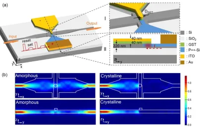
Fig. 1(a) shows the entire structure of the device. A regular silicon strip waveguide with a
width of 500 nm and a height of 220 nm is inserted with a 1×1 MMI-based waveguide crossing.
The MMI has a length of 12 m and a width of 2 m. The waveguides are connected to the MMI through 4-m-long tapers. The MMI crossing serves for two purposes. First, based on the self-imaging principle, the input light will be focused to the center of the MMI with a reduced
divergence angle. Therefore, light can go through the MMI crossing with a low insertion loss.
Second, the electrodes are placed on top of the silicon pads that are orthogonally oriented with
respect to the waveguide so that optical transmission through the MMI crossing can be
electrically controlled.
The inset of Fig. 1(a) shows the detailed structure of the MMI crossing. The P++-doped
silicon region is overlapped with the GST/ITO stack on top of the MMI crossing. The
overlapped region is a circular disk with an area of ×(DGST/2)2. Electrical pulses from the P++
-doped silicon go through the GST film and arrive at the ITO, causing ohmic heating and
therefore inducing phase change. The ITO layer also protects the GST from being oxidized
when exposed in the air. The GST/ITO layer thickness is 40 nm/40 nm.
To reset the GST from the crystalline phase to the amorphous phase, the GST is first melted
and then quenched rapidly by applying a high-voltage electrical pulse for a short time period.
To set the GST film back to the crystalline state, a medium-voltage electrical pulse is applied
to anneal the active region at a temperature between the crystallization temperature and the
melting temperature for a time period long enough to crystallize GST. In this way, we are able
to switch the material between its amorphous (low absorption) and crystalline (high absorption)
states in a non-volatile manner. Finite-difference time-domain (FDTD) simulations were
performed to calculate the light propagation through the MMI crossing. Fig. 1(b) shows the
cross-sectional electrical-field intensity (|E|2) distributions in the x-y and y-z planes when the
GST is amorphous and crystalline. It reveals a significant reduction in the waveguide
4
The fabricated process flow is described in the Supplementary materials. Fig. 2 shows the
overall and magnified images of a typical device after fabrication. The GST sandwiched
between the two electrodes has a size of DGST = 1 m.
Fig. 1. (a) Schematic structure of the GST-loaded silicon waveguide. The inset I shows the
zoom-in view of the active region. The inset II shows the transversal cross-sectional view of
the active region. (b) Simulated electric-field intensity distributions through the GST-loaded
[image:5.595.92.497.169.426.2]region when the GST is in amorphous and crystalline states.
Fig. 2. Optical microscope image of the fabricated device. The inset shows the zoom-in
scanning electron microscope image of the GST-loaded MMI crossing.
[image:5.595.90.506.526.676.2]5
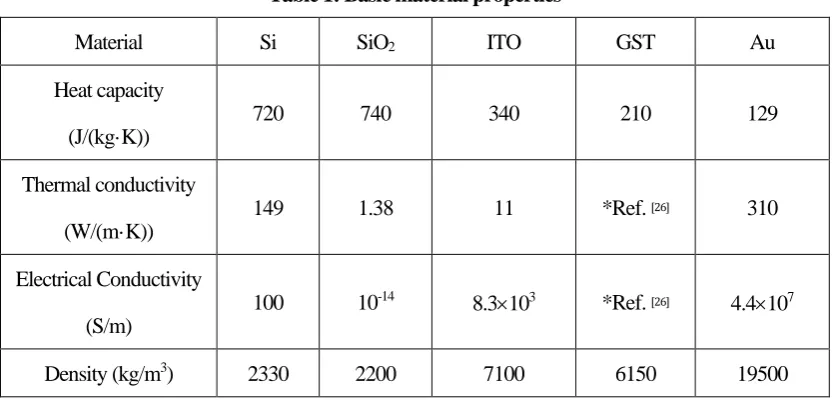
interactions in our device based on COMSOL Multiphysics. The electric currents and heat
transfer in solids modules were coupled via Joule heating and were employed to predict the
temperature distribution. Electrically insulating boundary conditions were applied to all
external boundaries except for the electrodes. The electrical contact impedance of P++-Si/GST
photonics, P++-Si/Au (~610-10·m2), and GST/ITO (~1.510-9·m2) were set according to
the measurement in test structures. The contact resistance measurement is described in the
supplementary material. The thermally insulating boundary conditions were used on all exterior
boundaries except for the bottom of the SiO2, where a constant temperature of T = 20 °C was
assumed (convective cooling by air and radiation cooling are insignificant). Table 1 summarizes
[image:6.595.90.507.321.521.2]the basic thermal and electrical properties of the materials used in this simulation.
Table 1: Basic material properties
Material Si SiO2 ITO GST Au
Heat capacity
(J/(kg·K))
720 740 340 210 129
Thermal conductivity
(W/(m·K))
149 1.38 11 *Ref. [26] 310
Electrical Conductivity
(S/m)
100 10-14
8.3103 *Ref. [26] 4.4107
Density (kg/m3) 2330 2200 7100 6150 19500
*The thermal and electrical conductivities of GST are not constant.
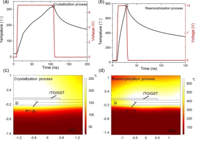
We first simulated the GST crystallization process, corresponding to the transmission
change from high to low. The simulation indicates that the temperature rises up to 300 °C, when
GST is driven by a set pulse with an amplitude of 7 V and a width of 100 ns. It is sufficient to
reach the GST crystallization temperature above 250 °C but below the melting point of 650 °C.
Fig. 3(a) illustrates the temperature change in response to the electrical pulse in the center of
the sandwich stack. Fig. 3(c) presents the temperature distribution at the falling edge of the
electrical pulse. We next initiated the re-amorphization process, where the GST was heated up
6
14 V and a width of 20 ns is applied, which raises the temperature above 700 °C in the GST
film. Fig. 3(b) shows the temperature distribution in the re-amorphization process. Fig. 3(d)
illustrates the corresponding temperature distribution.
Fig. 3. (a, b) Transient response of the temperature in the center of the P++-Si/GST/ITO
sandwich stack for (a) the crystallization process and (b) the re-amorphization process. (c, d)
Temperature distributions in the device cross-section at the end of the electrical pulses during
(c) the crystallization process and (d) the re-amorphization process.
Experimental results
The experimental setup used for device characterization is described in the supplementary
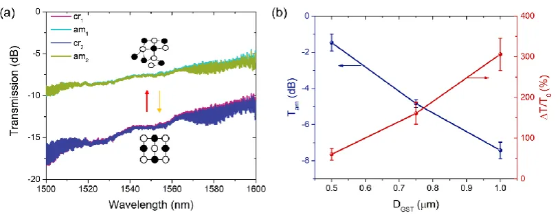
material. Fig. 4(a) shows the transmission spectra for two phase-change cycles (two crystalline
states and two amorphous states). The spectra were normalized to a reference straight
waveguide. The initial GST was crystalline, presenting a high transmission loss. The
re-amorphization of GST was then enabled by using a reset pulse. The transmission loss was
reduced from 14 dB to 7.5 dB at the 1550 nm wavelength. The heavy-doping induced loss is
[image:7.595.99.501.149.437.2]7
when the GST is amorphized. Further optimization of the overlap structure can reduce
excessive loss. The crystallization of GST was achieved by applying a set pulse, and the
transmission returned to the initial higher loss state. These processes can be repeated with no
significant degradation observed. We define the change in transmission as ΔT = (Tam-Tcr)/Tcr,
where Tam and Tcr are the transmissivities when the GST of the overlapped region is in the
completely amorphous and crystalline states, respectively [24]. It can be seen that ΔT is larger
than 300% for the 1-m-length GST. In fact, there is a compromise between the transmission loss at the amorphous state (Tam) and the change in transmission (T). As shown in Fig. 4(b),
the 0.5-m-long GST has a lower transmission loss of 1.5 dB but the change in the transmission is also reduced down to 52%.
Fig. 4. (a) Measured transmission spectra of the waveguide over two phase-change cycles. (b)
Transmission at the amorphous state and change in transmission between the crystalline and
amorphous states for three different GST lengths.
We next investigated the temporal response of the output transmission upon phase change.
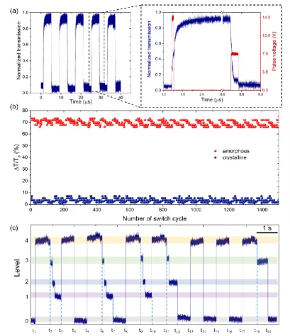
The probe light was fixed at 1550 nm. Fig. 5(a) shows the change in transmission upon repeated
switching between the crystalline and amorphous states of the GST. The results demonstrate
good reversibility and high transmission contrast of our electrically-driven GST. The
transmission can be maintained without any electrical current applied, exhibiting a good
‘self-holding’ feature. The inset shows the enlarged view of the electrical driving pulse and the
corresponding optical transmission change. The optical waveform is more complex as
[image:8.595.96.504.312.470.2]free-8
carrier generation, and thermo-optic effects that are all induced by the electrical pulses[18]. For
the response with the reset pulse (amorphization process), the transmission change is abrupt
after the electrical pulse, resulted from all effects. For the response with the set pulse
(crystallization process), two down-stairs were observed. The crystallization process at the first
stair was accomplished in 50 ns. The first down-stair represents the phase transition from the
amorphous state to the metastable crystalline state with a face-centered cubic structure. The
second down-stair represents the phase transition from the metastable crystalline state to the
stable crystalline state with a hexagonal structure. Fig. 5(b) shows that the performance of the
device is degraded after 1,500 switching cycles.
Our electrically-driven GST element cannot only realize binary switching but is also
capable of multi-level switching by controlling the degree of crystallization. Fig. 5(c) shows
the optical transmission dynamics in response to a sequence of set and reset pump pulses.
Multiple distinguishable intermediate levels are obtained due to the partial crystallization of
GST. The initial phase of GST is crystalline with low transmission (level 0). It returns to the
high level (level 5) after amorphization at time t1 using a single reset pulse with a width of 20
ns and an amplitude of 14 V. Three-level partial crystallization of GST is obtained from t2 to t3
by using a group of three set pulses. The period, width, and amplitude of the partial crystalline
pulses are 100 ms, 50 ns, and 5.2 V, respectively. The transmission returns to the high level
(level 5) after re-amorphization using a single reset pulse with a width of 20 ns and an amplitude
of 14 V. The intermediate level (level 1) after a group of three set pulses can further go down
to level 0 upon complete crystallization using a set pulse with a width of 100 ns and an
amplitude of 7 V as it occurs at t7. The transmission can also drop from other levels (level 4, 3
and 2) to level 0 by using a set pulse (t14, t19 and t12). We use the color-coded background to
mark the difference between the transmissions of any two consecutive levels. These exciting
results of our electrically-driven GST-enabled switch demonstrate that both set and reset
operations, to and from any intermediate level, are possible with accurate control of the
transmission levels and remarkable repeatability, just by applying the appropriate set or reset
electrical pulses. The number of levels is mainly limited by the noise of the photodetector.
Further reduction of the crystallization pulse power can give more levels. However, the
9
photodetector can help obtain more levels.
Fig. 5 (a) Temporal response of the device with the 1-μm-long GST changed between
amorphous and crystalline states. The inset shows the enlarged view of the driving electrical
pulses and the resulting optical waveform. (b) Transmission contrast over more than 1500
switching cycles. (c) Multi-level operation of the device showing the dynamic response to a
sequence of set and reset pulses.
[image:10.595.92.502.119.594.2]10
As shown in the supplementary material, the optical wave suffers a much larger change in
amplitude than phase when GST phase change occurs. A new optical phase change material
Ge2Sb2Se4Te1 [27], which exhibits significantly reduced optical attenuation compared to GST at
the 1550 nm wavelength and a remarkable difference in the real part of refractive index (n =
1.5), could be explored in the future work to get a larger optical phase variation with a lower
loss. Nevertheless, it is still possible to build a tunable coupler by varying the optical attenuation,
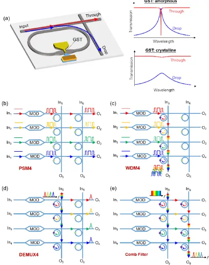
although its tuning range is limited compared to the phase tuning coupler. Figure 6(a) shows an
example of the 2×2 tunable coupler consisting of a waveguide crossing coupled with a silicon
microring resonator. The GST material is deposited on the ring waveguide to control the internal
loss of the resonator. When GST is in the amorphous state, the internal loss is small. As a result,
light can resonate in the microring resonator and is finally transmitted to the drop port. With
proper design, the critical coupling can be achieved, allowing for the complete elimination of
light from the through port at the resonant wavelength. On the other hand, when GST is in the
crystalline state, the internal loss increases considerably, destroying the resonances. The input
light thus travels to the through port. Therefore, upon phase change of GST, light from the input
port can be switched between the through port and the drop port.Variable optical power splitting
between these two ports can be achieved by partial crystallization of GST.
With this resonator-assisted tunable coupler, we conceive a silicon photonic chip that can
be reconfigured to various functions, as shown in Fig. 6 (b)-(e). For example, if we keep all
GSTs in the crystalline state, the input light from In1-4 will be modulated and guided to O1-4,
respectively. It thus forms a parallel single mode (PSM4) transmitter (Fig. 6(b)). If we keep all
GSTs in the amorphous state, the input light from In1-4 will be modulated and multiplexed to
O5. Hence, it becomes a wavelength-division-multiplexer (WDM4) transmitter (Fig. 6(c)).
Making use of the microring resonator cross-bar structure, we can achieve passive signal
processing functions such as wavelength demultiplexing (Fig. 6(d)) and comb filtering (Fig.
11
Fig. 6 (a) Schematic diagram of a 2×2 optical switch composed of a waveguide crossing
coupled with a silicon microring resonator. Light at the resonance wavelengths can be
switched between the through and drop ports, dependent on the phase state of GST. (b-e)
Illustration of a reconfigurable photonic circuit that can be programmed for multiple
functions: (b) PSM4 transmitter, (c) WDM4 transmitter, (d) de-multiplexer, and (e) comb
[image:12.595.93.502.79.597.2]12
Conclusion
We have demonstrated the non-volatile optical transmission control in a GST-clad silicon
waveguide. The active region is formed by a stack of P++-Si/GST/ITO films. Electrical pulses
applied to the stack can repeatedly change the phase state of GST. The static measurement
suggests that the device can operate over a bandwidth of more than 100 nm (limited by
measurement) and the transmission change can be >300% for 1-m-long GST. The temporal response measurements show that the transmission can be tuned in a controllable and repeatable
manner. In particular, multiple intermediate transmission levels can be obtained by partial
crystallization of GST. This successful implementation of a tunable silicon waveguide actuated
by electrically-driven GST marks a significant step forward in low-power and rewritable optical
circuits.
Acknowledgments
The authors would like to thank the support from the National Natural Science Foundation of
China (NSFC) (61535006, 61705129, 61661130155), Shanghai Municipal Science and
Technology Major Project (2017SHZDZX03). The authors also thank the Center for Advanced
Electronic Materials and Devices (AEMD) of Shanghai Jiao Tong University (SJTU) for the
support in device fabrications.
Disclosure of potential conflict of interest
The authors declare no competing financial interests.
References
[1] Heck MJR, Bauters JF, Davenport ML, et al. Hybrid silicon photonic integrated circuit technology. IEEE J Sel Top Quant, 2013, 19: 6100117-6100117
[2] Wang J, Long Y. On-chip silicon photonic signaling and processing: A review. Sci Bull, 2018, 63: 1267-1310
[3] Wang J. Chip-scale optical interconnects and optical data processing using silicon photonic devices. Photonic Netw Commun, 2016, 31: 353-372
[4] Zhuang L, Roeloffzen CGH, Hoekman M, et al. Programmable photonic signal processor chip for radiofrequency applications. Optica, 2015, 2: 854-859
[5] Capmany J, Gasulla I, Pérez D. The programmable processor. Nat Photonics, 2015, 10: 6 [6] Birth of the programmable optical chip. Nat Photonics, 2015, 10: 1
[7] Guo Z, Lu L, Zhou L, et al. 16 × 16 silicon optical switch based on dual-ring-assisted mach–zehnder interferometers. J Lightwave Technol, 2018, 36: 225-232
13
2018/05/13, 2018. Optical Society of America:
[9] Wang J, Huang H, Wang X, et al. Reconfigurable 2.3-tbit/s dqpsk simultaneous add/drop, data exchange and equalization using double-pass lcos and bidirectional hnlf. Opt Express, 2011, 19: 18246-18252
[10] Miller KJ, Haglund RF, Weiss SM. Optical phase change materials in integrated silicon photonic devices: Review. Opt Mater Express, 2018, 8: 2415-2429
[11] Miller KJ, Hallman KA, Haglund RF, et al. Silicon waveguide optical switch with embedded phase change material. Opt Express, 2017, 25: 26527-26536
[12] Wuttig M, Bhaskaran H, Taubner T. Phase-change materials for non-volatile photonic applications. Nat Photonics, 2017, 11: 465-476
[13] Xu P, Zheng J, Doylend JK, et al. Low-loss and broadband nonvolatile phase-change directional coupler switches. ACS Photonics, 2019,
[14] Zheng J, Khanolkar A, Xu P, et al. Gst-on-silicon hybrid nanophotonic integrated circuits: A non-volatile quasi-continuously reprogrammable platform. Opt Mater Express, 2018, 8: 1551
[15] Qu Y, Li Q, Cai L, et al. Polarization switching of thermal emissions based on plasmonic structures
incorporating phase-changing material ge2sb2te5. Opt Mater Express, 2018, 8: 2312-2320
[16] Kato K, Kuwahara M, Kawashima H, et al. Current-driven phase-change optical gate switch using indium–tin-oxide heater. Appl Phys Express, 2017, 10: 072201
[17] Stegmaier M, Rı ́os C, Bhaskaran H, et al. Thermo-optical effect in phase-change nanophotonics. ACS Photonics, 2016, 3: 828-835
[18] Tanaka D, Shoji Y, Kuwahara M, et al. Ultra-small, self-holding, optical gate switch using ge2sb2te5
with a multi-mode si waveguide. Opt Express, 2012, 20: 10283-10294
[19] Zhang H, Zhou L, Xu J, et al. All-optical non-volatile tuning of an amzi-coupled ring resonator with gst phase-change material. Opt Lett, 2018, 43: 5539-5542
[20] von Keitz J, Feldmann J, Gruhler N, et al. Reconfigurable nanophotonic cavities with nonvolatile response. ACS Photonics, 2018, 5: 4644-4649
[21] Zhang W, Mazzarello R, Wuttig M, et al. Designing crystallization in phase-change materials for universal memory and neuro-inspired computing. Nat Rev Mater, 2019,
[22] Chakraborty I, Saha G, Sengupta A, et al. Toward fast neural computing using all-photonic phase change spiking neurons. Sci Rep, 2018, 8: 12980
[23] Cheng Z, Rios C, Pernice WHP, et al. On-chip photonic synapse. Sci Adv, 2017, 3: e1700160 [24] Ríos C, Stegmaier M, Hosseini P, et al. Integrated all-photonic non-volatile multi-level memory. Nat Photonics, 2015, 9: 725-732
[25] Hosseini P, Wright CD, Bhaskaran H. An optoelectronic framework enabled by low-dimensional phase-change films. Nature, 2014, 511: 206-211
[26] Xiong F, Liao AD, Estrada D, et al. Low-power switching of phase-change materials with carbon nanotube electrodes. Science, 2011, 332: 568-570