Transfer-printed micro-LED and polymer-based
transceiver for visible light communications
K. R
AE,
1,*P. P. M
ANOUSIADIS,
2M. S. I
SLIM,
3L. Y
IN,
3J. C
ARREIRA,
1J. J. D. M
CK
ENDRY,
1B. G
UILHABERT,
1I. D. W. S
AMUEL,
2G. A. T
URNBULL,
2N. L
AURAND,
1H. H
AAS,
3AND
M. D. D
AWSON11Institute of Photonics, Department of Physics, SUPA, University of Strathclyde, Glasgow , UK
2Organic Semiconductor Centre, School of Physics and Astronomy, SUPA, University of St Andrews, UK
3LiFi R&D Centre, Institute for Digital Communications, University of Edinburgh, UK *[email protected]
Abstract: Visible light communications (VLC) is an emerging technology that uses LEDs,
such as found in lighting fixtures and displays, to transmit data wirelessly. Research has so far focused on LED transmitters and on photoreceivers as separate, discrete components. Combining both types of devices into a single transceiver format will enable bi-directional VLC and offer flexibility for the development of future advanced VLC systems. Here, a proof of concept for an integrated optical transceiver is demonstrated by transfer printing a microsize LED, the transmitter, directly onto a fluorescent optical concentrator edge-coupled to a photodiode, the receiver. This integrated device can simultaneously receive (downlink) and transmit (uplink) data at rates of 416 Mbps and 165 Mbps, respectively. Its capability to operate in optical relay mode at 337 Mbps is experimentally demonstrated.
Published by The Optical Society under the terms of theCreative Commons Attribution 4.0 License. Further distribution of this work must maintain attribution to the author(s) and the published article’s title, journal citation, and DOI.
1. Introduction
InGaN-based visible light emitting diodes (LEDs) are widely used in solid-state lighting and display technologies [1, 2]. Because of their high modulation bandwidth, ranging from 20 MHz for large-area LEDs [3, 4] up to several hundreds of megaHertz for microsize LEDs (µLEDs) [5, 6], they can also double as wireless transmitters in visible light communications (VLC) applications [7]. In particular,µLEDs have been demonstrated in VLC links with data transmission rates approaching 8 Gbps [6]. In a VLC system, LED transmitters are intensity modulated at high speeds and photoreceivers convert the optical signals into the electric domain. Research has so far mainly considered LED transmitters and photoreceivers as discrete devices. VLC demonstrations have also been principally unidirectional, the downlink using VLC and the uplink another technology like Wi Fi (wireless fidelity) or infrared communications. Here, in order to enable bi-directional VLC, we devise an integrated transceiver with aµLED as the transmitter. The signal-to-noise ratio (SNR) at the receiver and the overall bandwidth are key factors that affect the performance of VLC. Advanced modulation schemes, e.g. orthogonal frequency division multiplexing (OFDM), are often implemented in order to maximize utilization of the available bandwidth [6]. The size of the photoreceiver can be increased to enhance the SNR but this is at the detriment of the bandwidth as photoreceivers with large active areas tend to be slow [8]. One solution is to keep the active area of the receiver small and increase the amount of light arriving onto it with an optical element known as a fluorescent concentrator [9, 10], the downshifted light is waveguided to the edge of the concentrator where a small area receiver is positioned. Unlike lenses, these fluorescent concentrators make use of fluorescence (and an accompanying Stokes shift) and not exclusively reflection and refraction and can therefore be used to circumvent the étendue limit. This enables the collection of an incident signal over a wide
#346570 https://doi.org/10.1364/OE.26.031474
area and its concentration onto the detector whilst maintaining high bandwidth and excellent field of view of the receiver. In the following we report an integrated optical transceiver that combines a 450 nm transfer printed (TP)µLED (the transmitter) with such a fluorescent optical concentrator (the receiver). Transfer printing is a heterogeneous integration technique where micro- and nano-sized optoelectronic devices are ”printed” onto non-native, capability enhancing, substrates [11–19]. The advantage of a TPµLED is for integration of the transmitter with the concentrator receiver in a small form factor. Using a fullµLED-on-sapphire device, rather than a TPµLED, would lead to a device with at least twice the thickness and furthermore raise the issue of cross-talk at the receiver side. The performance of GaN-on-sapphireµLEDs for VLC is typically better than GaN-onSi devices [20] in terms of bandwidth and optical power. An alternative would be to transfer printµLEDs fabricated on sapphire and then released from their substrate by laser lift off [11]. On the other hand, the utilization of Si offers cost effectiveness, potential for scalability and a wide choice of substrate removal approaches. We note that TP
µLEDs used this demonstration have been shown to have modulation bandwidths of 100s of MHz, and data transmission rates of 120 Mbps on flexible and silica substrates [21, 22].
We describe the design and fabrication of an optical transceiver device and assess its operation using ODFM as the VLC modulation scheme. The device can simultaneously receive and transmit VLC signals, i.e. it can implement both the VLC downlink and uplink. It benefits from the wide-angle detection capability of the optical concentrator and can also operate as an optical relay, thereby providing a solution to the line-of-sight limitations of indoor communications [9].
[image:2.612.206.407.376.518.2]2. Design and fabrication
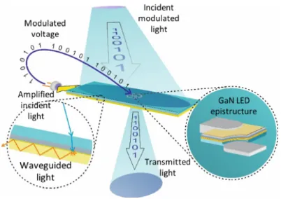
Fig. 1. Illustration of the optical transceiver concept. External modulated light is collected and concentrated by the optical antenna (fluorescent concentrator). This concentrated light is detected by an avalanche photodiode (APD) on the edge of the transceiver. For operation as a repeater, this signal is then demodulated, before being re-modulated and used to drive the transfer printedµLED transmitter.
The schematic in Fig. 1 shows the concept of the integrated optical transceiver device with the
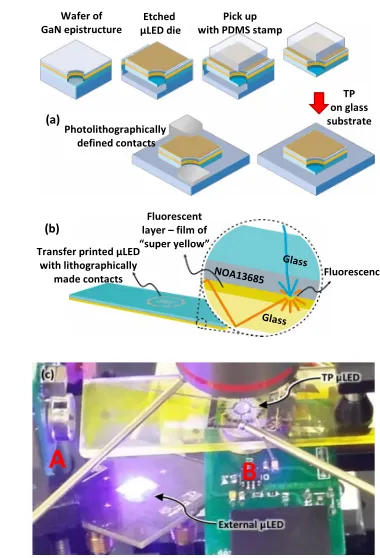
µLED on the top surface of the optical concentrator. Fabrication first entails TP the blue-emitting
µLED onto a 1 mm-thick 25 mm×75 mm glass substrate (microscope slide). TP makes use of the reversible adhesion of an elastomeric stamp to pick-up, transfer and print objects (here the
underetched with potassium hydroxide (KOH) to leave ultra-thinµLED platelets, suspended by 10µm-wide anchors that can be easily removed from their growth wafer with an elastomeric stamp. Figure 2(a) shows a schematic of the TP process. After TP, theµLED contacts are defined by photolithography [21]. Figures 3(a)–3(c) show microscope images of theµLED TP on the glass slide (seen on the bottom right of the three images) with metal tracks added. The metal track design gives scope to print a 6×6 array ofµLEDs, but this is beyond this first device demonstration. Figure 3(d) gives the current-voltage characteristic for such a TPµLED, these start to emit light around 3.5 V. It is important to note that theseµLEDs can have some leakage current, and so we only see light-emission after around 1 mA of drive current. This is possibly due to damage to the device sidewalls occurring when the Si substrate is removed, leaving a rough surface and increasing opportunities for tunneling. The current-optical power characteristic for these TPµLEDs is given in Fig. 3(e) and the emission spectrum when printed on the glass slide can be seen in Fig. 3(f). These TPµLEDs emit at 460 nm, and achieve over 50µW of optical power at 3.5 mA.
Before removal from their Si substrate, theseµLEDs have a lower turn on voltage and begin to emit light at around 2.8 V as reported in [21]. The optical power of 100 µm x 100 µm InGaN–on–SiµLEDs, fabricated in the same way but without any underetching of the Si substrate, is difficult to measure though, as the flip-chip configuration of theseµLEDs means light is not significantly transmitted until the Si substrate is removed. Top-emitting, broad-area,µLEDs processed on the same wafer as the TPµLEDs used in this work show a spectral emission around 450 nm. We attribute the 10 nm redshift between the spectral emission on Si and the TPµLEDs (see Fig. 3(f)) to strain effects induced when theµLED is removed from its growth substrate.
The glass substrate integrated with the TP µLED forms the top cladding of the transceiver. The other part of the transceiver is fabricated by blade coating a 70 nm-thick fluorescent film on a second microscope slide – this glass slide is the bottom cladding of the fluorescent concentrator, see Fig. 2(b). The fluorescent material is a conjugated poly (p-phenylene vinylene) copolymer, commonly known as “super yellow” (SY), acquired from Merck KGaA (PDY 132). The absorption and typical emission of SY respectively peak at 450 nm and 560 nm [25]. While we focus here on demonstrating a device concept and a stability study was not conducted, we did not observe any degradation of the fluorescence during experiments. We note that SY is a relatively stable copolymer, in widespread use in OLEDs, and given the device geometry, it is encapsulated by glass, which is beneficial for stability. Initially a 4 mg/ml solution of SY in chlorobenzene was prepared. An automatic film applicator (ZAA 2300, Zehntner GmbH) was used to blade coat the solution onto the glass. The temperature was set to 40◦C, the speed to 30
mm/s and the height of the blade (ZUA 2000.80) was 100µm above the microscope slide. A circular area (diameter 3 mm) of the SY film directly under the targeted position of the TP LED was mechanically removed. This is to prevent absorption ofµLED light emitted from the TP
Fluorescent layer – film of “super yellow”
Fluorescence
Glass Glass NOA13685
(b)
Wafer of
GaN epistructure μLED dieEtched
Photolithographically defined contacts
(a)
Pick up with PDMS stamp
TP on glass substrate
Transfer printed μLED with lithographically
made contacts
Fig. 2. (a) Illustration of the transfer printing process. (b) Schematic representation of the structure of the device. The inset shows the different layers of the fluorescent concentrator (Glass/Epoxy/Fluorescent medium/Glass). (c) Photograph of the setup used to characterize the optical transceiver device.
3. VLC demonstration and discussion
Two separate experiments were performed to demonstrate the capability of the transceiver device for VLC. The first consisted of operating the device to simultaneously transmit and receive independent data (transceiver mode). In the second experiment the device was operated to receive and re-transmit data (optical relay mode). In both these experiments, an externalµLED source (respectively blue, 450 nm, and 3 violet, 405 nm,µLEDs in series) and a second APD are used to respectively send a signal to and receive a signal from the transceiver. The typical electrical-to-optical modulation bandwidth of these external LEDs is above 100 MHz. The maximum optical power is approximately 9 mW at 175 mA and 9.5 mW at 45 mA for the blue and 3 series violet emitting LEDs, respectively. Information on the design, fabrication, and characteristics of the blueµLED used as an external source in this demonstration can be found in [26]. The power versus injection current for the 3 violetµLEDs is plotted in Fig. 4.
[image:4.612.207.397.100.379.2]Fig. 3. (a) and (b) photographs of the TP µLED and metal tracks on the fluorescent concentrator. (c) Photograph of TPµLED illuminating. (d) Current-voltage curve, (e) power-current curve, and (f) spectral characteristics of the TPµLED on the microscope slide.
Fig. 4. Optical power – current characteristic of the 3 violetµLED pixels in series used in the optical repeater demonstration.
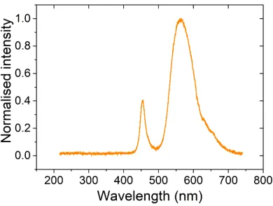
[image:5.612.221.392.397.540.2]link is referred to hereafter as link A, a spectrum of the light collected here is shown in Fig. 5. This shows a major peak at 563 nm from the color-converted SY light and a smaller peak at 543 nm from unconverted blue light from the incidentµLED . Light from the TPµLED (460 nm) is emitted down and straight through the glass and epoxy layers to the external APD at the position labeled B in Fig. 2(c). This optical link is referred to in the following as link B. The data rates given in the following are for a bit error rate (BER) target of 3.8×10⁻³[27]. The drive conditions in this first experiment are 6.1 V and 3 mA for the TPµLED and the 4.1 V and 24 mA for the externalµLED. The optical power of theseµLEDs is approximately 44.5µW for the TP
[image:6.612.209.404.223.370.2]µLED and 2 mW for the externalµLED at these drive currents. The typical electrical-to-optical modulation bandwidth for the TPµLEDs on glass is around 50 MHz [23].
Fig. 5. Optical spectrum of the light at the receiver (position B). The spectrum of the light transmitted by the device (at position A) can be seen in Fig. 3f).
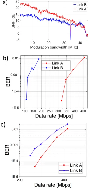
The SNR for both links is shown in Fig. 6(a). The higher SNR for link A is due to the higher optical power of the externalµLED. Figure 6(b) shows the data rates for both link A and link B. The link B with the TPµLED transmitter reaches a data rate of 165 Mbps. The link between the externalµLED and the transceiver (link A) has a data transmission rate of 416 Mbps. These performance values are consistent with the SNR of both links. The sharp drop in the SNR as the modulation bandwidth is increased past 40 MHz is attributed to the pulse shaping filter.
The second experiment demonstrates the integrated transceiver operating as an optical relay in decode and forward regime. The experimental setup is similar, but the external source is an array of 3 violet LEDs (405 nm) in place of the blue LED. The violet LEDs are used in this case to boost the received optical power at APD A. It also shows the wavelength flexibility at detection of the device while still demonstrating a viable VLC system, with violet LEDs an emerging enabling technology for white light solid state lighting as well as for communications [6, 28, 29]. The three violetµLEDs were driven in series, with a combined current of 30 mA (at 12V), the optical power of the three violetµLEDs was 7 mW. A lens (focal length 2.5 mm, diameter 2.5 mm) is also added onto the underside of the device, directly under the TPµLED, to increase the light collected by APD B. The emitted light of the external LEDs is collected by the fluorescent concentrator and detected at APD A. This detected signal is sent to an oscilloscope (MSO7104B) and demodulated offline in MATLAB, where all the signal processing operations are performed as described in [30]. The demodulated –QAM symbols are then remodulated and fed to the TP
a)
b)
[image:7.612.209.405.99.484.2]c)
Fig. 6. Transceiver mode operation; (a) The SNR of externalµLED (Link A) and TPµLED (Link B). (b) BER vs data transmission rates for link A and link B. (c) The BER results for link A and link B when the device is working as an optical relay. The dip in the SNR of both links seen in (a) around 35 MHz is an artefact from the measurement equipment used in this demonstration, and is not caused by the devices.
6(c). The optical relay functions at up to 337 Mbps, as it is limited by the speed of the slowest component – in this case the TPµLED. The improvement in data transmission rate from the TP
µLED (link B) between the first experiment (165 Mbps) and the second experiment (337 Mbps) is attributed to the integration of a lens to more effectively transmit light from the TPµLED to the APD.
arrays ofµLEDs, rather than a singleµLED as in this demonstration, will increase the light output power and therefore the range of the device. Additionally, increasing the light output power will increase the SNR, and consequently the data transmission rate. As seen in Fig. 3(e), theseµLEDs typically rollover at 4–6 mA, and so can’t be driven to high currents - limiting their power. Printing an array ofµLEDs would also go some way to negating this issue.
One of the main visions of VLC is that conventional room lighting can be used to transmit data through free space. We therefore chose here GaN-on-sapphireµLEDs as the external sources (rather than the sameµLEDs used for TP but before removal from their Si substrate) , as they are the conventional materials for solid-state lighting fixtures.
In any real-life VLC system, it would be important to minimize the required power of this device to integrate with other electronic components; one way to reduce this would be as in [33].
While this demonstration has focused on the VLC applications of this device, it could just as easily be applied to biomedical applications, such as optogenetics and biosensing, as demonstrated in [34–37], to wirelessly transmit signals to analysis equipment.
4. Conclusion
In conclusion, we have demonstrated, for the first time to our knowledge an integrated optical transceiver and repeater for visible light communications. The device is based on a transfer printed
µLED as the transmitter, and a fluorescent concentrator as the receiver. It was experimentally demonstrated that the optical transceiver can achieve beyond 100 Mbps data rates for reception and transmission. We believe that this new VLC device will be very suitable for implementing smart devices and enable IoT applications.
Supporting data can be found at DOI: 10.15129/7c4e99c7-94c5-4e69-b1b5-1d9e962cf164.
Funding
Engineering and Physical Sciences Research Council (EPSRC) (EP/K00042X/1).
Acknowledgments
The authors would like to acknowledge Erdan Gu, Xiangyu Wu, and Enyuan Xie for the fabrication of the externalµLED devices. IDWS is a Royal Society Wolfson research merit award holder.
References
1. S. Nakamura and M. R. Krames, “History of gallium-nitride-based light-emitting diodes for illumination,” Proceedings of the IEEE101(10), 2211–2220 (2013).
2. Y. Zhao, H. Fu, G. T. Wang, and S. Nakamura, “Toward ultimate efficiency: progress and prospects on planar and 3D nanostructured nonpolar and semipolar InGaN light-emitting diodes,” Adv. Opt. Photon.10(1), 246–308 (2018).
3. H. Haas, L. Yin, Y. Wang, and C. Chen, “What is LiFi?” J. Light. Technol.34(6), 1533-1544 (2015)
4. S. Rajbhandari, J. J. D. McKendry, J. Herrnsdorf, H. Chun, G. Faulkner, H. Haas, I. M. Watson, D. O’Brien, and M. D. Dawson, “A review of Gallium Nitride LEDs for multi-gigabit-per-second visible light data communications,” Semicond. Sci. Technol.32(2), 1–44 (2016).
5. J. J. D. McKendry, R. P. Green, A. E. Kelly, Z. Gong, B. Guilhabert, D. Massoubre, E. Gu, and M. D. Dawson,“High-speed visible light communications using individual pixels in a micro light-emitting diode array,” IEEE Photon. Technol. Lett.22(18), 1346–1348 (2010).
6. M. S. Islim, R. X. Ferreira, X. He, E. Xie, S. Videv, S. Viola, S. Watson, N. Bamiedakis, P. V. Plenty, I. H. White, A. E. Kelly, E. Gu, H. Haas, and M. D. Dawson, “Towards 10 Gb/s OFDM-based visible light communication using a GaN violet micro-LED,” Photon. Res.5(2), A35-A43 (2017).
7. H. Kopetz, “Real-time systems: design principles for distributed embedded applications,” Springer (1997). 8. “Hamamatsu Photonics: Si APD,” [Online] http://hamamatsu.com/jp/en/product/category/3100/4003/4110/index.html.
[Accessed: 27 Jan 2017].
9. P. P. Manousiadis, S. Rajbhandari, R. Mulyawan, D. A. Vithanage, H. Chun, G. Faulkner, D. O’Brien, G. A. Turnbull, S. Collins, and I. D. W. Samuels, “Wide field-of-view fluorescent antenna for visible light communications beyond the étendue limit,” Optica3(7), 702–706 (2016).
11. T.-I. Kim, Y. H. Jung, J. Song, D. Kim, Y. Li, H.-S. Kim, I.-S. Song, J. J. Wierer, H. A. Pao, Y. Huang, and J. A. Rogers “High–efficiency, microscale GaN light–emitting diodes and their thermal properties on unusual substrates,” Small8(11), 1643–1649 (2012).
12. R.-H. Kim, S. Kim, Y. M. Song, H. Jeong, T. Kim, J. Lee, X. Li, K. D. Choquette, and J. A. Rogers “Flexible vertical light emitting diodes,” Small8(20), 3123–3128 (2012).
13. S.-I. Park, Y. Xiong, R.-H. Kim, P. Elvikis, M. Meitl, D.-H. Kim, J. Wu, J. Yoon, C.-J. Yu, Z. Liu, Y. Huang, K.-C. Hwang, P. Ferreira, X. Li, K. Choquette, and J. A. Rogers “Printed assemblies of inorganic light-emitting diodes for deformable and semitransparent displays,” Science325(5943), 977–981 (2009).
14. A. De Groote, P. Cardile, A. Z. Subramanian, A. M. Fecioru, C. Bower, D. Delbeke, R. Baets, and G. Roelkens, “Transfer-printing-based integration of single-mode waveguide-coupled III-V-on-silicon broadband light emitters,” Opt. Express24(13), 13754–13762 (2016).
15. B. Guilhabert, A. Hurtado, D. Jevtics, Q. Gao, H. H. Tan, C. Jagadish, and M. D. Dawson, “Transfer printing of semiconductor nanowires with lasing emission for controllable nanophotonic device fabrication,” ACS Nano10(4),
3951–3958 (2016).
16. D. Kang, B. Gai, B. Thompson, S. M. Lee, N. Malmstadt, and J. Yoon, “Flexible opto–fluidic fluorescence sensors based on heterogeneously integrated micro–VCSELs and silicon photodiodes,” ACS Photonics3(6), 912–918 (2016).
17. D.-H. Kim, R. Ghaffari, N. Lu, and J. A. Rogers, “Flexible and stretchable electronics for biointegrated devices,” Annu. Rev. Biomed. Eng.14, 113–128 (2012).
18. S. Chary, J. Tamelier, and K. Turner, “A microfabricated gecko-inspired controllable and reusable dry adhesive,” Smart Mater. Struct.22(2), 25013 (2013)
19. C.-H. Cheng, T.-W. Huang, C.-L. Wu, M. K. Chen, C. H. Chu, Y.-R. Wu, M.-H. Shih, C.-K. Lee, H.-C. Kuo, D. P. Tsai, and G.-R. Lin, “Transferring the bendable substrateless GaN LED grown on a thin C-rich SiC buffer layer to flexible dielectric and metallic plates,” J. Mater. Chem. C5(3), 607–617 (2016).
20. P. Tian, J. J. D. McKendry, Z. Gong, S. Zhang, S. Watson, D. Zhu, I. M. Watson, E. Gu, A. E. Kelly, C. J. Humphreys, and M. D. Dawson, “Characteristics and applications of micro-pixelated GaN-based light emitting diodes on Si substrates,” J. Appl. Phys.115, 033112 (2014).
21. A. J. Trindade, B. Guilhabert, D. Massoubre, D. Zhu, N. Lauarand, E. Gu, I. M. Watson, C. J. Humphreys, and M. D. Dawson, “Nanoscale-accuracy transfer printing of ultra-thin AlInGaN light-emitting diodes onto mechanically flexible substrates,” Appl. Phys. Lett.103(25), 253302 (2013).
22. K. Rae, C. Foucher, B. Guilhabert, M. S. Islim, L. Yin, D. Zhu, R. A. Oliver, D. J. Wallis, H. Haas, N. Laurand, and M. D. Dawson “InGaN micro-LEDs integrated onto an ultra-thin, colloidal quantum dot functionalized glass platform,” Opt. Express25(16) 19179–19184 (2017).
23. A. J. Trindade, B. Guilhabert, E. Xie, R. Ferreira, J. J. D. McKendry, D. Zhu, N. Lauarand, E. Gu, D. J. Wallis, I. M. Watson, C. J. Humphreys, and M. D. Dawson “Heterogeneous integration of gallium nitride light-emitting diodes on diamond and silica by transfer printing,” Opt. Express23(7), 9329–9338 (2015).
24. K. Rae, E. Y. Xie, A. J. Trindade, B. Guilhabert, R. X. Ferreira, J. J. D. McKendry, D. Zhu, N. Laurand, E. Gu, I. M. Watson, C. J. Humphreys, D. J. Wallis, and M. D. Dawson “Integrated dual-color InGaN light-emitting diode array through transfer printing,” in the proceedings of IEEE conference on Photonics (IPC, 2015), pp. 390–391. 25. Sigma-Aldrich Super Yellow datasheet: www.sigmaaldrich.com/catalog/product/aldrich/900438?lang=en®ion=GB
(visited August 2018).
26. J. M. M. Santos, S. Rajbhandari, D. Tsonev, H. Chun, B. Guilhabert, A. B. Krysa, A. E. Kelly, H. Haas, D. C. O’Brien, N. Laurand, and M. D. Dawson, “Visible light communication using InGaN optical sources with AlInGaP nanomembrane downconverters,” Opt. Express24(9), 10020–10029 (2016).
27. F. Chang and V. S. Corp, “Forward error correction for 100 G transport networks,” IEEE Commun. Mag.48(3),
48–55 (2010).
28. P. F. Smet, A. B. Parmentier, and D. Poelman, “Selecting conversion phosphors for white light-emitting diodes,” J. Electrochem. Soc.158(6), R37–R54 (2011).
29. Soraa, blue–free lighting: www.soraa.com/learn/science/blue-free-light-what-you-need-know (visited August 2018). 30. D. Tsonev, H. Chun, S. Rajbhandari, J. J. D. McKendry, S. Videv, E. Gu, M. Haji, S. Watson, A. E. Kelly, G. Faulkner, M. D. Dawson, H. Haas, and D. O’Brien, “A 3-Gb/s single-LED OFDM-based wireless VLC link using a Gallium Nitride micro-LED,” IEEE Photon. Technol. Lett.26(7), 637–640 (2014).
31. S. Rajbhandari, A. V. N. Jalajakumari, H. Chun, G. Faulkner, K. Cameron, R. Henderson, D. Tsonev, H. Haas, E. Xie, J. J. D. McKendry, J. Herrnsdorf, R. Ferreira, E. Gu, M. D. Dawson, and D. O’Brien, “A multigigabit per second integrated multiple-input multiple-output VLC demonstrator,” J. Light. Technol.35(20), 4358–4365 (2017).
32. Z. Lu, P. Tian, H. Chen, I. Baranowski, H. Fu, X. Huang, J. Montes, Y. Fan, H. Wang, X. Liu, R. Liu, and Y. Zhao “Active tracking system for visible light communication using a GaN-based micro-LED and NRZ-OOK,” Opt. Express25(15), 17971–17981 (2017).
33. C. K. Jeong, K.-I. Park, J. H. Son, G.-T. Hwang, S. H. Lee, D. Y. Park, H. E. Lee, H. K. Lee, M. Byuna, and K. J. Lee “Self-powered fully-flexible light-emitting system enabled by flexible energy harvester, ” Energy Environ. Sci.7(12),
4035–4043 (2014).
35. S. H. Lee, K.-I. Park, C. Huh, M. Koo, H. G. Yoo, S. Kim, C. S. Ah, G. Y. Sung, and K. J. Lee “Water-resistant flexible GaN LED on a liquid crystal polymer substrate for implantable biomedical applications,” Nano Energy1,
145–152 (2012).
36. S. H. Lee, J. Kim, J. H. Shin, H. E. Lee, I.-S. Kang, K. Gwak, D.-S. Kim, D. Kim, and K. J. Lee “Optogenetic control of body movements via flexible vertical light-emitting diodes on brain surface,” Nano Energy44, 447–455 (2018).
37. H. E. Lee, S. H. Lee, M. Jeong, J. H. Shin, Y. Ahn, D. Kim, S. H. Oh, S. H. Yun, and K. J. Lee, “Trichogenic photostimulation using monolithic flexible vertical AlGaInP light-emitting diodes,” ACS Nano12(12), 9587–9595