Rochester Institute of Technology
RIT Scholar Works
Theses
Thesis/Dissertation Collections
8-1-1998
A Shared memory multiprocessor system
architecture utilizing a uniform
Frank Casilio
Follow this and additional works at:
http://scholarworks.rit.edu/theses
This Thesis is brought to you for free and open access by the Thesis/Dissertation Collections at RIT Scholar Works. It has been accepted for inclusion in Theses by an authorized administrator of RIT Scholar Works. For more information, please [email protected].
Recommended Citation
A Shared Memory Multiprocessor System Architecture
Utilizing a Uniformly Shared Level 2 Data-Only Cache
by
Frank Casilio
A Thesis Submitted
InPartial Fulfillment of the
Requirements for the Degree of
MASTER OF SCIENCE
InComputer Engineering
Approved by:
Committee Member:
Date:
~,
I
f?)
'9!J
l?
Roy S. Czernikowski, Professor and Department Head
Date:
Tony H. Chang, Professor
Committee
Member:---,---Department of Computer Engineering
College of Engineering
Rochester Institute of Technology
Rochester, New York
THESIS RELEASE PERMISSION FORM
Rochester Institute of Technology
College ofEngineering
A Shared Memory Multiprocessor System Architecture
Utilizing a Uniformly Shared Level 2 Data-Only Cache
I, Frank Casilio, hereby grant permission to any individual or organization to reproduce
this thesis in whole or in part for non-commercial and non-profit purposes only.
Frank Casilio
..
Abstract
Due to VLSI
lithography
problems and the limitation ofadditional architecturalenhancementsuniprocessor systems are nearingthe end oftheir life cycle.
Therefore,
it
is believed
that SymmetricMultiprocessing
(SMP)
systems will be the next mainstreamcomputer. These systems allow multiple processors, accessing the same memory
image,
tocooperateon a number of computationaltasksasa single entity.
While multiprocessor systems can offer a substantial performance increase
compared to uniprocessor systems, major design considerations must be addressed to
achieve desired system efficiency levels.
Managing
cache coherenceis
a significantproblem in multiprocessor systems. Current
implementations
cope with this problemby
utilizing a cache coherence protocol. This protocol puts a large amount ofoverhead on
the systembusto ensureproper program execution, effectively
decreasing
overall systemperformance. This thesis approaches the cache coherence problem from a new angle.
Instead ofutilizinga cache coherenceprotocol, a newmemory system
is
proposed whicheliminatestheneed fora cache coherenceprotocol,
by
utilizing asharedlevel 2data-only
cache. This new architecture allows for better utilization ofthe system and
improved
performance and scalability.
A data rate analysis
is
conducted todemonstrate
the potential performanceincrease from the proposed architecture over conventional approaches. The
data
ratemodel clearly shows an increase
in
system performance and utilization when using thearchitecture proposedinthis thesis.
To
My
Parents,
withouttheirconstantloveand
supportthismilestonein my career could not
have beenaccomplished
Acknowledgements
I would
like
to thank thefollowing
individuals for their supportduring
thecompletion of this thesis.
First,
and foremost I would like to thank my graduatecommittee members, Dr.
Roy
S.Cznernikowski,
Dr.Tony Chang,
and especially Dr.Muhammad Shaaban forthe
help
andinsighthe offeredintothis thesis.Secondly,
I would like to thank all ofmy professors, managers, coworkers, andpeers who have given me the privilege to
learn,
experience, and grow with themduring
Trademarks
Intel,
Pentium aretrademarksofIntel CorporationTable
ofContents
Abstract iii
Acknowledgements v
Trademarks vi
TableofContents vii
ListofFigures ix
ListofTables x
ListofEquations ~ xi
Glossary
xii1 Introduction 1
1.1 VLSI Advancements 2
1.2 Architectural Advancements 4
1.2.1
Pipelining
41.2.2 Branch Prediction 6
1.2.3 SuperscalarDesign 7
1.2.4 Cache 7
1.3 Flynn's ClassificationofComputer Architectures 11
7.3.7 SISD 12
1.3.2 MSD 12
1.3.3 SIMD 13
1.3.4 MLMD 13
1.4 TheQuestforaMainstreamSupercomputer Architecture 14
1.4.1 SMP 75
2 Cache Coherence 19
2.1 CacheBasics 20
2.7.7 CacheOrganization 20
2.1.1.1 Direct MappedCache 21
2.1.1.2FullyAssociative 21
2.1.1.3 Set Associative 22
2.7.2 CacheBlock
Lookup
222.1.3 Replacement
Strategy
232.1.3.1 LeastRecentlyUsed(LRU) 23
2.1.3.2Random 24
2.1.3.3Fiist-In,First-Out(FIFO)
'.'"'"'"".^24
2.1.4 Write
Policy
242.1.4.1 Write-Through 24
2.1.4.2Write-Back
ZZZ^25
2.2 MultiprocessorCachecoherence 25
2.2.7 Data
Sharing
262.2.2 ProcessMigration 26
2.3 WaystoHandleCache Coherence 27
2.3.7
Directory
Based Protocols 272.3.2
Snoopy
BusProtocols. 282.3.2.1 Write-InvalidatePolicy 29
2.3.2.2 Write-UpdatePolicy 29
2.3.2.3 Write-Once Protocol 30
2.4 Consistency Models 31
2.4.1 Sequential
Consistency
312.4.2 Weak
Consistency
333 DesignofMPArchitectures 35
3.1 Current MultiprocessorImplementation 35
3.7.7 TheChipset 36
3.1.1.1 Circuit Switched Buses 37
3.1.1.2 Split TransactionBus 38
3.7.2
Memory
Type 393.1.2.1 ReadingaCache BlockFromMemory 40
3.7.3 The MESICacheCoherence Protocol 41
3.2 ProposedMultiprocessor Architecture 43
3.2.7 Cache Arbitration Unit(CAU) 46
3.2.2 SharedL2*Cache 47
3.2.3 SharedL2*bus 48
3.2.4 Processor Requirements 48
4 Performance Analysis 50
4.1 Performance Analysis Methods 50
4.2 Data Rate Analysis 51
4.2.1 Data Rate Analysis for CurrentSMP
Memory
System's 524.2.2 Data Rate Analysis oftheProposedArchitecture 54
4.2.3 InvalidationOverhead. 54
4.2.4 Comparison ofData Rate Models 58
5 Conclusions 63
5.1 Future Work 64
6 References 65
List
ofFigures
Figure 1-1:Grand ChallengeApplications 1
Figure 1-2:
Chip Density
forIntel Microprocessors -2Figure 1-3: ProjectedCPU
Frequency
fornext15years 3Figure 1-4: Fivestagepipeline -5
Figure1-5:
Memory
Hierarchy. 9Figure 1-6: Cache EffectonaSystems Performance 11
Figure 1-7: Block Diagram ofanSMPSystemwith4 Processors 15
Figure 1-8: CacheeffectonaSMPsystem 16
Figure 2-1: Cache Organization Schemes 21
Figure 2-2: A Typical Cache Block Address 22
Figure 2-3: Data
Inconsistency
duetoDataSharing
26Figure 2-4: Data
Inconsistency
duetoProcess Migration 27Figure 2-5: Initial State ofthe
Memory
System 28Figure 2-6:State oftheSystemafter a Write-lnvalidationOperation 29
Figure 2-7:State ofthe
Memory
Systemafter a Write-UpdateOperation 30Figure 2-8:State Diagram forthe Write-Once Protocol 31
Figure 2-9: The Sequential
Consistency
Model 32Figure 2-10: The TSO Weak
Consistency
Model 34Figure 3-1: The Intel DualPentiumII Processor
Memory
System 36Figure 3-2: A Circuit SwitchedBus 38
Figure 3-3: ASplit Transaction Bus 39
Figure 3-4: The MESI Write-Invalidate Protocolwith Write-Back 41
Figure 3-5:Modified Architecture toSupportaL2*Cache 44
Figure 3-6: Modificationto theCPU
Packaging
45Figure 4-1: Data Rate ofaTypical Program 52
Figure 4-2:Program Data Rate ofCurrent SMP
Memory
Systems 53Figure 4-3: Program Data Rate ofProposed
Memory
System 54Figure 4-4: Effect ofInvalidationonCacheMisseswhile
Varying
BlockSize 56Figure 4-5: Effect ofInvalidationonCache Misseswhile
Varying
Cache Size 57Figure 4-6: Effect ofData
Sharing
onBus Utilization 58Figure4-7: Performance ComparisonwhenProgramsExhibitFine Grain
Sharing
61Figure 4-8: Performance DifferencewhenPrograms Exhibitper-processor
locality
62List
ofTables
List
of
Equations
Equation1:
Mapping
for BlockinaDirect Mapped Cache 21Equation2:
Mapping
for BlockinaSetAssociativeCache 22Equation3:Execution Time fortheCurrentArchitecture 59
Equation4:ExecutionTime fortheProposed Architecture 60
Glossary
Bus,
Aset ofconductors connecting varies functionalunits in a computer. A shared memory
bus
specificallydenotes
abus
connectingtheprocessorsto thechipsetBranch
Prediction,
Amethodto predict the destination of conditional branch instructions to reduce stalls in
the
instruction
pipelineCache,
A relatively small amount of high-speed memory that contains
frequently
usedinstructions
and data. It is intendedto reducethe accesstimesto the next higherlevel ofthememory
hierarchy
Cache
Coherence,
A problem which occurs in multiprocessor systems when multiple private caches have
differentvalues ofthesame cacheblock
Cache
Hit,
The data blockrequested
by
theprocessor existsincacheCache
Miss,
Thedatawordrequested
by
theprocessordoes not existin cache. Theentire cacheblockcontainingthedataword mustbereadfromthenexthigher level ofmemory
Central
Processing
Unit(CPU),
Responsible for processing
instructions
in the computer system and managing cache coherenceinmultiprocessor systemsChipset,
Responsible for controlling all major
functions
in computer systems. The chipset controls allaccesstomemoryand controlsthesystembusCircuit Switched
Bus,
Abus arbitration scheme which givesthebus master exclusivecontrol overthe
bus
untilitsrequest
has
been filledConsistency
Model,
Specifies the order
by
which the eventsfrom
one process shouldbe
observedby
otherprocesses
in
themachineDirect Mapped
Cache,
A cache organization that allows ablock to
be
placed in a specific location only insidethecache
Dynamic Random Access
Memory
(DRAM),
Atype ofsemiconductormemory in which the information
is
stored in capacitors on aintegrated
circuit.Typically
each bit is stored as an amount of electrical charge in a storage cell consistingof a capacitor and atransistor.Extended Data Out Dynamic Random Access
Memory
(EDODRAM),
Allows the data outputs from memory to be kept active after the control signals have gone
inactive.
This can be used in pipelined systems foroverlapping accesses where thenext cycle
is
startedbeforethedata fromthelastcycle isremovedfromthebus.First-In,
First-out(FIFO)
Replacement,
Acacheblock replacement strategythatremovestheblockthathas beenthe cache forthe longestperiod oftime
Fully
AssociativeCache,
Acache organizationthatallows ablocktobe placed anywhereinsidethe cache
Least
Recently
Used(LRU)
Replacement,
A cache block replacement strategy that removes the block which has not been used in
thelongestperiod oftime.
Level 2
(L2) Cache,
Asecond level of cachethat existsbetweentheprocessor and main memory
Massively
Parallel Processor(MPP),
A computer system made from commodity processors that uses physically distributed
memorytoachieve ahigh levelof parallelismthroughahigh
bandwidth
interconnectMultiprocessor
(MP),
See Symmetric
Multiprocessing
MultipleInstruction MultipleData
(MTMD),
Eachprocessorfetches its own instructionand operates onits own data
MultipleInstruction Single Data
(MISD),
Eachprocessorfetches
its
owninstruction,
but
all processors operateonthe samedata
Pipelining,
An architectural enhancement wheremultiple
instructions
areoverlappedin
executionRambus DRAM
(RDRAM),
Intendedtoreplace
SDRAM in future
computer systems. Itoffers sustainedtransferratesofaround
1000Mbps,
sofaster buses
canbe
implemented.Random
Access
Memory
(RAM),
A
data
storagedevice for
whichthe order ofaccessto different locationsdoes
not affectthe speed of access
Reduced
InstructionSet
Computer(RISC),
A processor whose
design is based
on the rapid execution of a sequence of simpleinstructions
ratherthanontheprovision of alarge
varietyof complexinstructionsScalability,
The measureof
how
systemperformanceincreasesas system resources areincreased
Set
AssociativeCache,
Acache organization which
divides
the entire cacheinto
separate setswhich canhouse
aspecific setof
blocks
Single Instruction
Single
Data(SISD),
See
UniprocessorSingle Instruction Multiple Data
(SEVfD),
The sameinstruction
is
executedby
multiple processorsusingdifferent
dataSnoopy
Bus,
A
bus based
protocol, commonly utilizedin
shared memory multiprocessor cachecoherence protocols
Split Transaction Bus
(STP),
Abusarbitration scheme
by
which a masterdoes
nothold
ontothebus if
the slavedevice
cannot respond immediately. Instead control
is
givento anotherdevice
which can useit
atthatmoment
Superscalar,
An architectural enhancement
for
microprocessorsby
which multipleinstructions
areprocessed simultaneously using
dynamic scheduling along
withcompileroptimizationsSymmetric
Multiprocessing (SMP),
A system configuration
in
which all multipleidentical
processors are connectedtogetherviathe same shared
bus
andhave
equalaccesstoallresourcesSynchronous Dynamic Random Access
Memory
(SDRAM),
A form ofDRAM which adds a separate clock signal to the control signals.
SDRAM
chips can contain morecomplexstatemachines,
allowing
them to support "burst" accessmodesthatclock out aseries ofsuccessive
bits
Uniprocessor,
Acomputerthat
has
only
one processorWrite
Back,
A
caching
mechanism where cacheblocks
are written back to the next levelin
thememory
hierarchy
onlywhenneededWrite-Once
Protocol,
Acache coherence mechanismwhich
forces
a cacheblocktobe
writtenback to the nexthigher level
ofmemory onlyafterthefirst
writeby
theprocessorWrite
Invalidate,
Atypeof cache coherenceprotocolthat
invalidates
all other copies ofthe cacheblockin
otherprocessor'sL2cache
Write
Through,
A cachingmechanism
by
which cacheblocks
arewrittenbackto thenext higherlevel
ofmemoryafter each writetothecacheblock
Write
Update,
A type of cache coherence protocol that updates all other copies ofthe cache block
in
other processor'sL2 cache
Very
LargeScale
Integration(VLSI),
Aterm
describing
semiconductorintegrated
circuits composed ofhundreds
ofthousandsof
logic
elements ormemorycells.1
Introduction
Forthepast 20years the
majority
ofimprovements in computinghas
comefrom
more powerful processors. In today's information age computing power
is
being
challenged at all
levels,
from
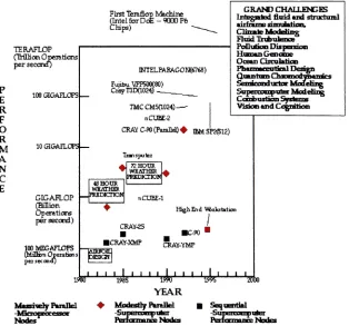
multimedia applications to the grand challenge problems.The President
instituted,
in
1992,
thefive-year federal
High PerformanceComputing
andCommunications
Initiative. Thishas
spurred the development of advanced processortechnology
and wasinitially
focused
on the solution ofthe grand challenges shown inFigure
1-1. These are fundamental problems in science and engineering, withbroad
economic and scientific
impact,
whose solution could be advancedby
applying highperformancecomputingtechniquesand resources.
FirstTferaflopMachine
ntelfb hips)
g
op Ma oE-t IntelfbrDcE-TOO Ft
TERAFLOP (Trillion Operations persecond) P E R F O R M A N C E 100 GIGAFLOPS 10GIGAFLOPS GIGAFLOP (Billion Operations persecond) 100 MEGAFLOPS (MiHrtiOperation: peisecondj INTFXFAEAGOH(S7S8) Fujiisu.VPF500(80) CKj-nDdOM) TMCCM5C102* nCUBE-2 CRAYC-#>(Faialld)^ EMSF2C512) GRAND CHALLENGES Integratedfluidand structural airframesumnaiioD* Fluid Trubulence Pollution Dispersion Human &enome OceanCirculation Pharmaceutical Design QuantumChromod^iarrics SerriicoTMiuctarModeling Combustion Systems VisionandCognition
GJHOUR .WEflTHER . IPKBEK3KIN 72 HOUR WEATHER FREPKn'ION tiCUBE-1
High End WtksMimi
CRAVES
C-M CRAy-XM? CRAr-YMP 8IRKI
DJfciKJi
i*r' ' 'tis' "li1 " 'ilk1 " 3Dbo YEAR
[image:17.577.134.448.338.631.2]MtssToeryPiraflel ? ModestlyParallel Sequential ^ficroprocessor -Supercomputer -Supercomputer
What
was once considered a supercomputer dedicated to solving particularproblems, now
functions
in
tiny
handheld devices.
Hence,
theneedfor
faster processorswill always exist.
The ability
to produce faster processorshas
been possibledue
to advancesin
VLSI
(Very
LargeScale
Integration)
technology
andcomputer architectureoverthe past20years.
1.1
VLSI
Advancements
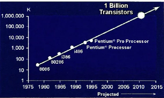
In 1965 Gordon Mooreobservedthat thenumber oftransistorsper squareinchon
integrated
circuitshad doubled
every year since the integrated circuit was invented.Moore predictedthat this trendwouldcontinue forthe
foreseeable
future. In subsequentyears, the pace slowed down a
bit,
but data
density
has doubled
approximately every 18months. Tothispointthat
theory
has
heldthrough andin many casesthe actualincrease
has
exceeded Moore's prediction. Figure 1-2[INTEL]
shows the transistor count forIntelmicroprocessorssince the mid-1970's.
1 Billion _,
V
1.000,000 -,
\
Transistors
100.000 - ^^
10.000
-0**Pentium-Pro Processor 1,000 -^ idftfi Pentium- Processor 100 -*s I^*i386 30286 10 -1 -19 8086 75 1 1980 1 1985 1 1990
i i t i
1995 2000 2005 2010 2015
[image:18.577.147.431.447.617.2]Projected *
At
the current rate ofgrowth, processors with 1 billiontransistors should surfacearound 2010. Atthis point, clock
frequencies
of processors willbe
around 10GHz asshown
in Figure
1-3[INTEL].
MHz
uu.uuu-10.000-
10GHz^^-
1,000-
100
-Pro -Processor
^"HpPentium
-Processor 9***^*i486"'-'Processor
10-m J> i386"; rZ>rfr 80286
"
Processor
1 -8086
0.1
-r i 1 1 i 1 !
00 Projected
Figure 1-3: ProjectedCPU
Frequency
fornext 15yearsThisexponential
increase
has beenaccomplishedby
theincredible
advancementsin VLSI technology. The
feature
size of modern computershas
reached the 0.25Dmmark and
is
dropping
further. Thissmallerfeature
sizehas
alloweddesigners
toproducesmaller, cooler processorswithahigherclock
frequency.
However,
it is believed
thatcurrentlithography
techniquesfor
silicon will notbe
applicable at
feature
sizesless
then 0.1 Dm. Evenwith a 0.1Dmfeature
size, 1billion
transistors would occupy an enormous amount of space and consume a
large
amount ofpower. It
is
predictedthat within the next 5 years current siliconVLSItechnology
willreach
its limit.
Once
this pointis
reached an alternative toSilicon,
such as GalliumArsenide
(GaAs),
willbe
needed.However,
this newtechnology
would requirecomprehensive modification of current VLSI
technology
and a completeretooling
offabrication
facilities,
which would take an outrageous amount oftime
and money.This
leaves
architectural advancements as the onlyviable alternative to achieve higher levelsofperformance.
1.2 Architectural Advancements
The second reason thatmicroprocessors were ableto
keep
up with the desire formorepower
is due
to the advancementsin computer architecture. Computerarchitecturedeals
largely
withtheinstruction
set architecture, and performance enhancementissues ofCPU design.
There have beena number ofdramaticchangesto CPUarchitecture sincethefirst
IC-based CPU was created. The list below
is
by
no means a complete list ofadvancements incomputer architecture,but it serves as a point of referenceto the impact
that architectural advancementshavemade.
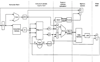
1.2.1
Pipelining
Pipelining
has had the most dramaticimpact
on the performance of the CPU.This architectural improvement
is
an implementation technique that exploits parallelismamong instructions in a sequential
instruction
stream. Ithas
the substantial advantagethat, unlike some speedup techniques, it is not visibleto theprogrammer. Most modern
processors use sometype oflinearsynchronouspipelinewith added
features
such as dataforwarding
andbranchprediction.A linear pipelined processor
is
a cascade ofprocessing
stages that arelinearly
connected to perform a
fixed function
over astream ofdata
flowing
from
one endtotheother. The
intent is
tobe
able tointroduce
anewinstruction into
the pipeline at everyclock cycle sothatno stage
in
the pipelineis
everyleft idle.
Ifthisis
accomplished thenAs stated previously, linear pipelined processors are constructed with k
processingstages. External
inputs
(operands)
arefed intothepipeline atthe first stageS;.The processed results are passed
from
stageSi
to stageS;+l,
for all i=l,2,...,k-l. Thefinal
result emerges at thelast
stage, Sk. Each resultis
passed to the next stage baseduponthe clock cycle ofthe pipeline.
Ideally,
we expect the clock pulses to arrive at allthe stages at the same time.
However,
due to a problem known as clock skewing thesame clockmayarrive atdifferentstages with atimeoffset. To avoidthis theclock cycle
ofthepipeline mustbethecombined maximum ofthe executiontime ofthelongest stage
ofthe pipeline and
its
clock skewed offset. Theblock diagramof a five stage pipeline isshown in Figure 1-4 [HENPAT96].
Instructionfstch
PC
Aed NiPC
tnstrurton memory
rosier?etofc
FteClsirc
-0--~tiH
<6 /&nr.\32
:xeai'e' gikkass
r Zero? Branch
Cond
u
)ALU ALU
ouSJUt
Memory
access
a
Dais
ternary MD
WiSe back
Figure 1-4:Fivestage pipeline
Each stage ofthe pipeline performs one part ofthe processing of an
instruction.
[image:21.576.86.493.335.590.2]While
pipelining
has resultedin
a tremendous increase in the throughput of aCPU,
it
has alarge
amount ofoverhead associated withits
implementation. In addition,resource and
data
dependencies
among the instructionsbeing
processed in the pipelineprevent
full
utilization ofthe pipeline. This manifests itself in terms of pipeline stallcycles.
Therefore,
pipelining
complicates the traditional processorby introducing
theneed for additional advanced architectural concepts such as data
forwarding
and branchprediction.
1.2.2 Branch Prediction
Data
dependencies
and branch instructions limit the performance of pipelinedprocessors dueto the additional logicneeded tocope withthem. Branch instructions are
verycommonin any process dueto the behavioroftheprogram
being
executed. When apipeline
is
full and a branch is encountered the address of the next instruction to beprocessed is not known until the previous instruction has finished executing since the
processor condition codes will not have been set correctly yet. When a branch is
encountered a branch prediction unit
is
responsible to pick the nextinstruction
tobe
executed in the pipeline. There are many advanced algorithms for choosing the correct
instruction,
based
on the pasthistory
ofexecution. This architectural enhancementis
essential to maintainthe throughputofthepipeline at an acceptable
level.
Some branch
prediction schemes
have been
ableto reach95% accuracy. Ifthewrongbranch is taken,
the pipeline must be
flushed
and executionis
restartedfrom
thelast
correctinstruction
1.2.3
Superscalar
Design
Superscalar designs
incorporate
additional functional units that are used toprocess a number of
instructions
simultaneously. These processors aresometimes calledmultiple-issue processors, since more than one instruction can
be
issued to functionalunitsin a single clock cycle. The processor
issues
avarying number ofinstructions perclock, which may
be
statically scheduledby
the compiler ordynamically
scheduled.Usually,
theseinstructions
mustbe independent
and will have to satisfydependency
constraints. Such
dependency
constraints include resource, control and datadependencies. Ifsome instruction
in
the instruction streamis
dependent or doesn't meettheissuecriteria, onlythe instructions proceedingthatone inthe sequence willbe
issued,
hence the variability in issue rate. Most modern processors have a superscalar
design,
with some
being
able to issue up to 6instructions
at once if the conditions areappropriate.
1.2.4
Cache
Along
the same lines as pipelining cache has an enormousimpact
on thethroughput of a CPU. In the earliest microprocessor days
instructions
and data werestored inmain memorywhich
is
notlocateddirectly
ontheprocessor chip. Thisinvolves
incurring latency
due to the memory access time. Whendealing
with main memory,latency
canlead
to a lot of processor idle time since an external memorybus
accessrequest
is
issued.To deal with
this,
a small,fast
chunk ofmemoryis
placed close to theCPU
tohold intermediate datathatmightbe needed again soon. This small amount ofmemory
is
Locality
statesthatmost programsdo
notaccess all code or datauniformly. Thisprinciple, plus theguideline that smallerhardware
is
faster,
ledto thehierarchy
based onmemories of
different
speeds and sizes. Since fast memoryis
expensive, a memoryhierarchy
is
organized into several levelseach smaller, faster and more expensive perbyte
than thenextlevel. Thegoalis
toprovide amemorysystem with cost almost as lowasthe cheapestlevel ofmemory and speed almost as
fast
as thefastest level. The levelsof
hierarchy
usually subset one another; all data in one level is also found in the levelbelow,
and alldata inthelowerlevel is found inthe onebelowit.The memory
hierarchy
of a computer system starts atthe processor level with itsinternal registers. These are the fastest and easiest forthe processor to access. Next in
lineistheLevel 1
(LI)
cache stored onthe same dieastheprocessor. This level of cachealso
has
avery lowlatency
sinceit is operating atthe same speed ofthe chip. The Level2 cache, which isthe nextlevel inthe
hierarchy,
canbe on the same package asthe CPUor onthemainboard. Ineither case
it
has ahigherlatency
since data must comethroughthe memory bus into the CPU. Main memory is the next level and is much larger
(by
many orders of magnitudes) than L2 cache. Programs that are currently running are
stored in main memory and are accessed throughthememory bus when
they
areneeded.Hard disk
is
generally considered the lowest level onthe memoryhierarchy
chain. Thislevel
is
the largest andby
far the slowest level sinceit involves
an actual physicalmovement ofthereadhead. Figure 1-5 gives avisual
depiction
ofthe memoryhierarchy
Room
Box
Board
Begfie Chip
Cache
MainMemory
[image:25.577.180.394.48.398.2]Secondary Memory
Figure 1-5:
Memory
Hierarchy
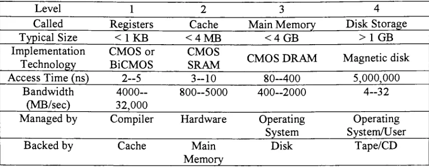
Table 1
[HENPAT96]
showsthe rangeofsizesand access timesof eachlevel in
Level 1 2 3 4
Called Registers Cache Main
Memory
Disk StorageTypical
Size
<1KB <4MB <4GB >1 GBImplementation
Technology
CMOS or
BiCMOS
CMOS
SRAM CMOS DRAM Magnetic disk
Access Time
(ns)
2-5 3-10 80-400 5,000,000Bandwidth
(MB/sec)
4000-32,000
800-5000 400-2000 4-32
Managed
by
Compiler HardwareOperating
System
Operating
System/User
Backed
by
Cache MainMemory
[image:26.576.68.509.60.233.2]Disk Tape/CD
Table 1: Rangeofsizes and accesstimesineachlevel inthememory
hierarchy
The need for cache
is
due to the factthe CPU performance has advanced fasterthan memory performance. CPU performance has improved 35% per year until
1986,
55%per yearsince, whilememoryperformanceimproved only 7%per year. Withthis in
mind, cache has proven to be a very effective way to improve overall system
performance.
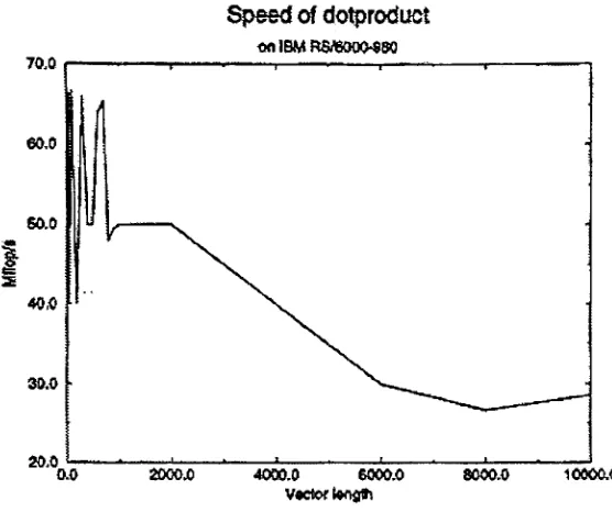
Figure 1-6 shows the speed ofthe
dotproduct,
oftwo vectors on the cache basedRS/6000-980. For vector lengths greaterthan 2000 the cache cannot accommodate all
relevant data and the performance drops as more data has to be transported to/from
memory.
70,0
60.0
60.0
I
40,0
30.0
20,0
Speedofdotproduct
onlBMRSraooOSW
200O.0 4000.0 6000.0 vcstftfl*
[image:27.576.145.423.62.295.2]8000.0 10000.0
Figure 1-6: CacheEffecton aSystems Performance
While,
each of these enhancementsindividually
can increase processorperformance, modern processors use them all to make an extremely advanced design.
These enhancements, coupled with VLSI
technology
advancements, have made itpossible for computingpowertogrow at an exponential rate.
1.3 Flynn's Classification
ofComputer Architectures
All uniprocessor systems follow the von Neumann model. The von Neumann
architectureis characterized
by
aCPU and central memory system, withinstructions
anddata
being
readfrom memory.Afteraninstruction has beenreadthe
instruction is decoded
and thenany relevantoperands fetched from memory, the
instruction is
executed andthe result stored back inmemory. The single
data
pathbetween
theCPU
and memory over whichboth
instructions and
data
must pass, and the sequential nature ofinstruction
executiontogether limit the performance possible
from
the computer. Thisis
sometimes known asthe von Neumann
bottleneck.
Thisis
aided in uniprocessor'sby
pipelining andsuperscalardesign enhancements.
One
form
of classificationforvonNeumann machines is based onthe number ofinstructions
that can be executed at any one time and onthe number of chunks ofdatathat can be operated on at atime. In 1972 Michael Flynn introduced a classification of
various computer architectures based on notions ofinstruction and data streams. The
number of
instructions is
given as either SI for single instruction or MI for multipleinstructionand the number ofpieces ofdata is given as either SD forsingle data orMD
formultipledata. Machinescanthus beclassified as
SISD, MISD,
SIMDorMTMD.1.3.1
SISD
The classical von Neumann machine can be regarded as a
single-instruction-single-data machine in that at any one time only a single instruction
is
being
executed,and only a single piece ofdata
is
being
operated upon. Thisis wherepart ofthe problemarises, since we often want to performthe same instruction on many different pieces of
data,
andthevonNeumannmachine requires ustofetchthe same instruction manytimes,
once for each piece ofdata. In fact the situation is much worse since a von Neumann
machine will usually require us to create a
loop,
and so we will need to execute manyinstructions for each piece of data. This can slow the machine down many times over
whatthearithmetic unit
is
capable ofperforming.1.3.2
MISD
The multiple instruction single
data
(MISD)
architectureis
the most uncommonone. Inthis architecture,the same
data
streamflows
throughalinear
arrayofprocessors,executing
different instructions
onthe stream. This kindof architectureis
also known asa systolic array for pipelinedexecution of specific algorithms.
1.3.3
SIMD
Forproblems inwhich the same operation needs to be performedon many pieces
of
data,
particularly thoseinvolving
vectors and arrays, SIMD (single-instructionmultiple-data) architectures are often capable ofhigh speeds. A single CPU controls
many arithmetic units, each of which operates on
its
own data. Each arithmetic unitexecutesthe same instruction as determined
by
theCPU,
but uses data found inits
ownmemory. Thus all the elements oftwo vectors could be added together simultaneously,
increasing
the speed oftheoperation manytimesover a SISDmachine.Inpractice, theprovision ofmany arithmetic units
is
expensive, particularly sincemany ofthemwill notbe in use atanygiventime. Evenifalarge number of arithmetic
units are provided, the size of vectors and arrays will rarely be amultiple ofthe number
ofarithmetic units and so some
inefficiency
intheuse ofthearithmetic units will arise.A more effective use of hardware can be obtained
by
pipelining the arithmeticunit. A hardware
floating
point accelerator will already contain dedicated hardware foreach part ofthe calculation of a
floating
point operation.By
pipelining the use ofthishardware,
significant improvements can be made in processor performance. Thistechnique will not give as high a performance as a true SIMD machine,
but
theimprovementscanbesignificant.
1.3.4 MIMD
The most general
form
of vonNeumann architectureis
themultiple-instruction-multiple-data machine. A MTMD machine
is
usually a number of separate processorsconnected together through some interconnection network. The actual format of
interconnection between
the processors can take manyforms, depending
on the type ofproblem, whichthe machine
is
designedto solve. Thisis
the most common architecturechosen for multiple processor machines
because
modern processors have the controllogic for parallel systems
built
in.
Therefore,
this is attractive since software,replacementparts and additionsto the system areeasilyaccessible.
1.4 The Quest for
aMainstream Supercomputer Architecture
As stated previously CPU performance advancements have come from two main
areas, VLSI and computer architecture improvements. It seems certain that the
advancements in VLSI technologies are
hitting
the limits.Also,
most architecturalenhancementshavebeen implemented incurrentdesigns. Withthisinmind, thefutureof
mainstream computing
is
in need of an alternative computer platform. This alternativelies inparallel processing. Parallel processing
involves
utilizingmorethan one CPU inacomputersystem; working cooperativelyto achieve
increased
performance. As shown inthe previous sectionthere arefour architectures that couldbe usedto
implement
parallelmachines. It is believed that the appropriate choice for future machines will
be
oftheshared memory MIMD "tightly-coupled" variety.
These
systems will usually containbetween 2 to
O(10)
CPU's on a single systemboard
with uniformly shared memorybetween the processors and an interconnection network on the
board.
Boards
ofthisnature are referredto as
"tightly-coupled"
due to the
fact
that the processorslie
closetoeach other on the same system board.
Systems
createdin
this nature are referred to asSMPmachines.
1.4.1
SMP
An SMP node contains several identical processors, each
typically
with its ownon-chip cache and a larger off-chip cache, which have uniform access to a shared
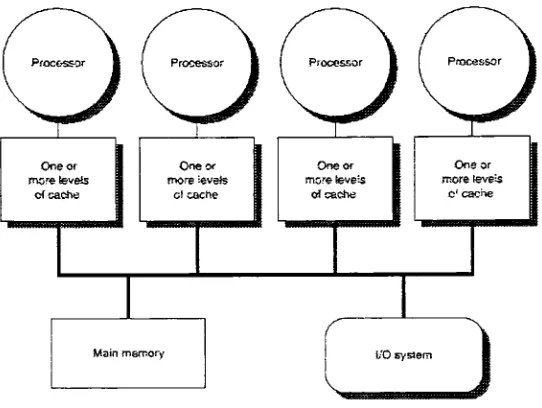
memory and other resources such as the network interface. Figure 1-7 shows a block
[image:31.576.153.424.193.397.2]diagramof asymmetricmultiprocessing system.
Figure 1-7:Block Diagramof anSMP Systemwith4 Processors
In this scenario there are four processors each of which
has
their own local L2cache outside ofthe CPU in addition to the LI cache
inside
ofthe processor. In SMPsystems each processor sharesthe samememory
image.
This means thatif
twodifferent
processors accessed the same memory
location,
they
would receiveidentical
values.Some importantcharacteristics ofSMP's include:
High-Speed
Memory
Bus - Since severalprocessors need to get access to main
memory, a
dedicated,
high-throughput memorybus
is
required.Design
ofthe memorybus
is
criticalin
producinganefficient SMP architecture.Separate
Secondary
Cache
-Each
processor
in
the systemhas
its
own secondary(level
2)
cache.The
provision of separate cachesfor
each processor requires complexlogic
in the cache controllerto make sure that a processor never works ondata
thathas
been
updatedin
another processor's cache. This problemis
addressed through cache coherence protocols that make sure the most recent value in the processors cache correspondsto thedata in
memory. The primary advantageofa dedicated-cache designis
the ability toincrease
the number ofprocessors in a system, without saturating thememory
bus.
This approach seems tobe
the most popular for high-end multiprocessor serversbecause it
ensures optimum performance even when a systemis
scaled toits
maximum configuration. The size ofthe cache itself
is
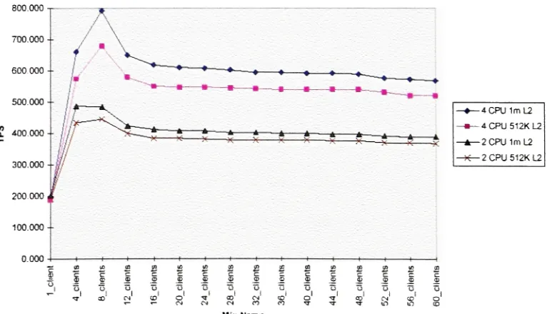
also relevantto performance. Asa general rule, the larger the secondary cache, the better an SMP system will scale as extra processors are added. Figure 1-8 showsthe effect in TPS
(transactions
per second) ofon-chip cacheinanSMP systemwithtwoandfourprocessors.800.000
700.000
600 000
500.000
-400.000
--300.000-
-200.000
100.000-p
-
-*--* ?
* tr *
*-* * * M X * X * *^K-* * A
-4CPU1mL2 -4CPU512KL2 -2CPU1mL2 -2CPU512KL2
0.000 H 1 1
1-X i J) JI 10 X Si
c = c H e c: e B
t>
2
CI CO O T CD CM <D O V CO1 CM* <u' o' MixName
Figure 1-8:Cacheeffecton aSMPsystem
[image:32.577.100.483.420.640.2]I/O to
Memory
Bus Bridge - Insystems
today
the I/O bus interfaces with thememory bus rather than
directly
to a CPU. This creates even more contention in SMPsystems since the CPU'smust go through
it
to access resources. Therefore ahigh speedI/Oto
Memory
Bus Bridgeis
required.Multiprocessor systems will be the main thrust once VLSI and architectural
advancements have reached the end oftheir lifetime. These systems will be found in
homes
and businesses alike.The MTMD architecture seems to be the future ofmainstream high performance
computing.
However,
it involves
system design complexity. Amajor obstacle in thesesystems
is
cache coherence. Since there are multiple processorsworking cooperativelyon a single or multiple tasks, data
is
constantlybeing
shared between the processors.Whenone processor makes a changeto some piece of shared
data
(currently
stored in itslocal cache) the other processors needto know about
it
in casethey
will need to use thesame piece ofdata. Ifother processors are not informed
immediately,
the value for thedatathat
they
usemay notbethemost current. Thisproblemis called cache consistency.To alleviate this problem current systems use a cache coherence protocol to
insure
thatthe data in a processors local cache is always up to
date.
This extra processing andmemory bus access results in a large amount of overhead for SMP systems.
Unfortunately,
there are no currentimplementations
that can alleviate this problem.Instead current systems aim to deal with the problem
in different
ways,resulting in
alargeoverheaddueto the coherenceprotocols used.
This thesiswill present a new architecture
for
multiple processor systems, whichremovesthe cache coherence protocol required
in
sharedmemory MTMD architectures.In chapter
2,
we will investigate cache coherence and the various approaches tocope with it. We
follow
by focusing
chapter 3 on analyzing the current MTMDarchitectures versus the proposed architecture. Then in chapter 4 we will compare
benefits
gained from using the new architecture alongwith the changes that need to bemadefor ittobe
implemented
feasibly. Tothis end, adatarate model ofSMP systemsisemployed to
illustrate
performance of each ofthe architectures.Finally,
chapter 5 willconcludethethesis and present
directions
for futurework.2
Cache
Coherence
As
discussed in
section 1.2.4, L2 cache existsbetweentheCPU and main memoryin a computer system. The purpose ofL2 cache
is
to further reduce effective memoryaccesstime
by
reducingthe LI cache misspenalty, since main memory's speed is muchslowerthan thatoftheCPUs internalregisters andLI cache.
Inuniprocessorsystems, cacheis easily implementedwithverylittle added design
overhead and complexity. Whenthe processor needs information that does not exist in
its internal registers orLI cache
it
checks for the datain theL2 cache. Ifthe data doesnot existin L2 cache,then thedata isreadfrom main memory, which may inturnneedto
gotoa mass storagedevicetoretrievethe
information,
generating a pagefault. Ifa pieceof
data
is found inacacheit isconsidered a cachehit,
otherwiseit is
a cache miss. Cachemisses are simplyone minusthe cache
hit
ratio, whichis
the ratio ofthenumber ofitems
that arefound in cache versus the number of
items
requested. Once thedata is found
inmemory it istransferred toL2 cacheintheform of a cacheblock. Whentheprocessor is
finished using a piece of
data,
itis
updated in LI and L2 cache. Main memoryupdatesdepend onthe actual write policyused, either write-through orwrite-back,
discussing
insection 2.1.4. This method of program execution
is
thebackbone
of all uniprocessor'sfollowing
thevonNeumann model.A sufficiently
fast
memorybus
mustbe
implemented
between
L2 cache and mainmemorytomeetthe
demand,
for instructions
anddata
by
theprocessor.2.1
Cache Basics
Beforethe cachecoherenceproblem can
be
detailed itis
importantto have a goodunderstanding ofhow caches handle data. The memory
hierarchy
of computers breaksinformation
upinto
toblocks ofdata. These blocksofdataare movedin and out of cacheas needed. An entireblockof
data (which includes
many memorylocations)
is moved ata
time, due
to the principle of spatial locality. Spatiallocality
states that items whoseaddresses are near one anothertend tobe referenced closetogether intime [HENPAT96].
Therefore,
when a new block is broughtinto
the cache itis
beneficial tobring
in thesurrounding data also, since
they
will mostlikely
be needed in the near future. Thedesignof cache subsystems involves fourmajorissuesthatneedtobeaddressed.
2.1.1
Cache Organization
The organization of a cache dictates where a block can be placed when it is
brought in from main memory. There are three cache organizations used today: direct
mapped,
fully
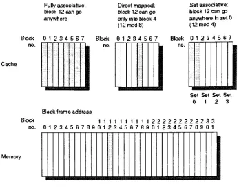
associative, and set associative. Figure2-1 visually describes each ofthreeorganizations. Their descriptionsare containedinthe
following
section.FuHyassociative:
block 12can go anywhere
Directmapped:
block 12can go
onlyintoblock 4 (12mod8}
Setassociative;
block12canga anywherehset0
(12mod4)
Block 0 12 345 67 Block 0 12 34 5 67 Block 01 2 345 6 7
Cache
n
Set Set Set Set
0 12 3
Blockframeaddress
Block 1111111111222222222233
no. 01234567890123456789012345678901
[image:37.576.114.461.60.336.2]Memory
Figure 2-1:CacheOrganizationSchemes
2.1.1.1 Direct MappedCache
In a directmapped cache, each block has only one place where
it
can gointo
thecache. The mapping forablock
in
adirectmapped cacheis
shownin Equation 1.(block address) MOD (number of blocksincache)
Equation 1:
Mapping
forBlock inaDirect Mapped Cache2.1.1.2
Fully
AssociativeIn a
fully
associative cache, eachblock
can appear anywherein
the cache.Fully
associative caches are extremely easy to
implement,
because
ofthe minimal amount ofoverheadinvolved.
2.1.1.3 Set Associative
Finally,
set associative caches, limit the number of places ablock can be placed.Blocks inthe cache arebroken offinto groups of sets. Each block inmemory
is
mappedinto
a single set, generally using Equation 2.(block address) MOD (number ofsetsinthecache)
Equation2:
Mapping
for Block inaSet Associative CacheOnce amemory block has beenassignedto asetitcanbeplaced anywhere inside
theset.
2.1.2
Cache
Block
Lookup
Nowthat it is understood how caches get data into
them,
the process ofreadingfrom a cache will be detailed next. Each block in a cache has an address
tag
associatedwith it. When a processor wishes to retrieve data from the cache it uses the block's
address
tag
to reference the data. Thetag
of each block (the actual number ofblockschecked depends upon the organization of the cache)
is
compared against thetag
requested
by
theCPU. The figure belowshows layoutof anaddress forpiece ofdata
in acache.
Blockaddress Block
offset
Tag
IndexFigure2-2:ATypicalCacheBlockAddress
The index portion ofthe address
is
used to select the setin
the cache, while theblock offset
is
usedto selectthe actual piece ofdata
in the cacheblock. Thetag
portionoftheaddress
is
comparedto theprocessors requestedtag.A
fully
associative cache wouldhave
no index field since ablock is not restrictedto any single set.
Note
thatin
a set associative cache the index field would be used toselectthe setthatcontainsthedata. While
in
adirect
mapped cachetheindexfield
wouldselecttheactual
block
containingthedata.2.1.3
Replacement
Strategy
The replacement strategy
dictates
which blockis
replaced when a cache missoccurs. The actual process of selecting the block to be replaced when a cache miss
occurs
is
doneby
the cache controller. A cache miss occurs when thetag
requestedby
the CPU was not
found
inthe cache. When a miss occurs, ablock inthe cache mustbereplaced with a block from the next higher level of memory. In a direct mapped cache
thereis no need fora replacement strategy sincethere is onlyone locationthat ablock is
capable ofgoing into. There are many replacement strategies that are used in cache
controllers. Threereplacement strategies are
Least-Recently
Used, Random,
andFirst-In,
First-Out(FIFO).
2.1.3.1 Least
Recently
Used(LRU)
The LRU replacement strategy records all accesses to cache blocks. When a
cache miss occursthecacheblock that
is
replacedis
theonethathas
gone unusedforthelongest amount of time. This
follows
along the samelines
as temporallocality.
Temporal
locality
statesthata cacheblockthathas been
recentlyusedis
likely
tobe
usedagain in the nearfuture. LRU replacement can
become
extremely expensive, especiallyin
largecaches, since all accesses needtobe
recordedinternally
in
thecache.2.1.3.2 Random
The simplest strategy to employ
is
a random replacement strategy thatis
spreaduniformly across the cache. When a cache miss occurs a random block number
is
selected and the selected block
is
replaced. Studies have found that while the randomreplacement strategy may not be the most intuitive strategy
its
results are quiteimpressive.
The attractiveness in a random replacement strategyis
in the ease ofimplementation.
2.1.3.3
First-In,
First-Out(FIFO)
FIFO replacement strategyreplacesthecacheblockthat has been in cacheforthe
longestperiod oftime. This strategy has provento yield worse resultsthan theLRU and
random replacement strategies.
2.1.4 Write
Policy
The final aspect about caches
is
the write policy. When a data valuehas
beenmodified in the processor registers, it is
immediately
written back to LI cache and L2cache.
Updating
the data in main memory depends on the particular write policybeing
employed inthe system. Therearetwowritepoliciesthatare used incache
design
today.2.1.4.1 Write-Through
In a write-through cache, when data
is
written to L2 cacheit is
also written tomain memory simultaneously.
Therefore,
main memory always contains an exact copyofthe datathat is in the L2 cache ofthe processor.
Write-through
cache's put alarge
amount of overhead onto the memory bus since
it is
not always necessary tohave
anupdated copy ofthe
data in
main memory. Forthis reason, write-through caches are notwidely used.
However,
writethrough caches are extremely easy toimplement
since allwrites aresenttoL2 andmain memoryatthesametimeand no additional logic
is
neededin
the cache.2.1.4.2
Write-Back
Inwrite-back caches, data iswrittenback only to theL2 cache. Whenthe cache
becomes
full or the cache block isbeing
replaced, the data is then updated in mainmemory.
Therefore,
all writing to main memory from L2 cacheis
done when a cachemiss is encountered. The advantage ofthe write back cache
is
that all writes from theprocessor occur
locally
at the speed of the cache memory (much faster than mainmemory). Since main memory
is
only updated when the cache block is needed, thememory bandwidth requirements of a writeback policy are much more lenientthan that
ofthe write-through policy. This frees up bandwidth for other devices in the system,
most
importantly,
other processors inmultiprocessor systems.2.2 Multiprocessor Cache
coherenceIn a multiprocessor system, data
inconsistency
can occur in adjacent levels ofmemory or within the same level.
Therefore,
it is possible for the current data in mainmemory to differ for its most recent value, sincethe most recent value would
be
storedonly in theprocessors local cache
(depending
onthewritepolicy,it
may alsobe
in mainmemory). In addition, L2 caches of otherprocessorsmay contain even older
data
valuesofthe same memory location. Thisis not possible
in
uniprocessor systems sincethereisonly one processorin the systemthatwill ever modify the
data.
There aretwo possiblewaysinconsistent
data
can appearinacache,data
sharingorprocess migration.2.2.1
Data
Sharing
Since
datain
multiprocessorsystemis
commonly sharedbetween manyprocessesexecutingon
different
processorsit is
possiblefortheprivate caches on each processortocontain
different
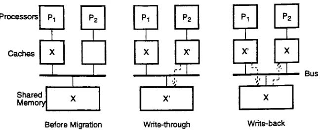
copies ofthe same shared data. Figure 2-3[HWANG93]
shows howinconsistency
can occur whendealing
with shareddata.
Processors
Pi p2 Pi p2 Pi p2
1
1
Caches X X X'
X X"
X
\'-i
1
Shared
Memory x
X'
X
Beforeupdate Write-through Write-back
Bus
Figure 2-3: Data
Inconsistency
duetoDataSharing
2.2.2 Process Migration
In multiprocessor systems, processes
frequently
migratefrom
one processor toanother.
Unfortunately,
shareddata
thatis
residing in aprocessor's local cachedoes
notmigrate withthe process.
Therefore,
it is
possible foraprocessorto updatea shareddata
value in
its
L2 cache, getinterrupted,
hand the process over to the OS which in turnhands
it
overto anotherprocessor. Thisproblemis
knownas process migration andis
acommon occurrence resulting
in data
inconsistencies.
Figure 2-4[HWANG93]
visuallydepicts
how data becomes
inconsistentdue
toprocess migration.Processors
Caches
Pi p2
X
Shared Memory
Pi p2
X X
rJ
X'
Pi P2
X X
,
i
rJX
Bus
[image:43.576.119.444.52.191.2]BeforeMigration Write-through Write-back
Figure 2-4: Data
Inconsistency
duetoProcess Migration2.3 Ways
to
Handle Cache Coherence
Multiprocessor systems have widely varying ways to handle inconsistent data in
memory. In massively parallel processors
(MPP's)
a directory-based schemeis
used,whilein SMP systems snoopy busprotocols are used.
2.3.1
Directory
Based Protocols
Directory
based coherence protocols are commonly used in large scale,distributed memory systemswhere afast interconnectionnetwork exists between each of
the nodes. In a distributed
directory
scheme eachmemoryunithas
adirectory
structurewhich contains listings of which cache currently has copies of
its
memory blocks. Whena read miss occurs in a cache, a request message is sent to the memory unit that
it
received the cache block from. The memory unitthen updates
its
valuefrom
the cachewith the most current copy and sends a copy to therequesting cache. Central
directory
based schemes have a main
directory
which contains all theinformation
relating to amemory block's location
in
a processor's cache. Lookups aredone
using this centraldirectory
only. Contention onthe centraldirectory
has limited
adaptation ofthis schemein actual systems.
2.3.2
Snoopy
Bus Protocols
SMP systemsuse shared memoryconnectedto ahigh-speed memory bus. These
systems also
follow
the von Neumann model of execution, allowing all the CPU's toaccess the main memory asynchronously with respect to each other. In parallel
applications data sharing between processes running on different CPU's requires
advanced
features
tokeep
data
coherent.Since caches are used inthese
designs,
therewillbedata
consistencyproblems inmain memory since themost recent datavalues wouldbe stored in caches. Tothis end,
SMP systems employ a cache coherence mechanism to ensurethat the value a processor
is reading from its cache is the most current one. Cache coherence requires both
hardware and software supportto achieve acceptablelevels inperformance.
The hardware support for cache coherence comes in the form of a snoopy
bus,
operating under a snoopy-bus protocol. When multiple private caches are tied together
on a single
bus,
the methods used to ensure consistency entail changes to the writepolicies. The snoopy bus allows all processors inthesystemto monitorthe traffic on the
memory bus. The processor is allowed to take appropriate action
depending
upon thewritepolicy. Figure 2-5 shows a SMP system with ashared memoryvariable
loaded into
each oftheprocessor's local caches.
Shared
Memory
Bus
Caches
[image:44.576.180.395.565.652.2]Processore
Figure 2-5: Initial Stateofthe
Memory
SystemInthenext sectionswe will seehowthe caches and memoryare modified to cope
with cache coherence.
2.3.2.1 Write-Invalidate
Policy
In a write-invalidatepolicywhen a processor writes a valueto a cacheblock in its
private cache it also sends an invalidation signal to all other caches which contain the
cache
block,
including
main memory. This signal notifies them that the data haschanged.
X"
*
Shared
Memory
1 1 1
Bus
1
1
1X1
1 Caches
[image:45.576.179.395.300.385.2]A
fa)
d)
ProcessorsFigure 2-6: StateoftheSystemafteraWrite-Invalidation Operation
Figure 2-6
[HWANG93]
shows the state ofthe system after a write-invalidateoperation,
by
Pi.
Since thePi
has a write through cache, main memory contains theupdated valuethat itreceived overthe snoopy bus from
Pi.
2.3.2.2 Write-Update
Policy
In awrite-update policy when aprocessor writes a value to a cache
block
inits
private cache it also updates other caches (if
they
contain the cacheblock)
and mainmemorywith the new value. The update
is done
using thefeatures
ofthe snoopybus,
which allows other processors to monitor
bus
activity. Figure 2-7[HWANG93]
showsthe state of a SMP system after the write-update operation, in which all caches now
containtheupdated value.
X Shared
Memory
1 1
1
Bus
1
1
1
X X" X'
Caches
[image:46.576.180.404.161.247.2]Processors
Figure 2-7: Stateofthe
Memory
Systemafter aWrite-UpdateOperationThe write-update policy is extremely effective at ensuring data consistency.
However,
it places anunnecessarily largeamount oftraffic onthe memory bus since notall processors mayneedthe updated value.
2.3.2.3 Write-Once Protocol
James Goodman in 1983 proposed a cache coherence protocol for bus-based
multiprocessors. Inordertoreduceunnecessary bus
traffic,
theveryfirst
write of a cacheblockuses a write-through policy. Thiswill
keep
main memory consistent with the localcache afterthe first write. Afterthefirst write, memory
is
updated using the write-backpolicy [GOOD83]. Figure 2-8
[HWANG93]
details
Goodman's protocol, which uses 4statesto describes
its
execution.P-Read Write-lnv/Read-lnv
P-Write Read-lnv
[image:47.576.198.380.64.240.2]P-Write
Figure 2-8: StateDiagram fortheWrite-Once Protocol
Each transaction in the figure represents extra overhead that is placed on the
memory bus. This traffic reduces the amount of utilization of the bus
by
otherprocessors,whichinturndegradestheoverallperformance ofthemachine.
2.4
Consistency
Models
Parallel applications executing on a parallel machine require data to be used in
multiple CPU's. Because ofthis it is very important to make other processors aware
about any changes to data that
they
may also have a copy.Consistency
models specifythe order
by
whichtheeventsfrom
one process shouldbe observedby
other processes inthe machine [Hwang93]. The two main consistency methods are sequential and
weakened consistency.
2.4.1
Sequential
Consistency
Sequential consistency
is
when"theresultofanyexecution[of
theprogram]is
thesame as
if
the operations of all processors were executed in some sequential order, andthe operations of each individual processor appear
in
this sequencein
the order specifiedby
its
program"[LAMP79].
Since data is loaded and storedidentically
to uniprocessorsystemsthe coherencemechanism mustbe abletorespond rapidlyto changes.
Processors
switch
Single-PortMemory Shared
Memory System
Figure 2-9: The Sequential
Consistency
ModelFigure 2-9
[HWANG93]
shows how the sequential consistency model can bedescribed. Eachprocessor
is
connectedtomemorythroughthe same switchensuringthatno processor can update mainmemoryout of order.
Thesingle portedmemory ensuresthat thereis only one memoryaccess operation
inprogress at anyonetime. Therefore some queuing mechanism is needed to order and
serializethememoryreferences while
they
waittobe serviced.In 1992
Sindhu, Frailong,
and Cekleov specified that for sequential to exist thefollowing
five
axiomsmustbetrue [SINDHU92]:1)
A loadby
a processor always returnsthevalue writtenby
thelatest storetothesame locationby
otherprocessors.2)
The memoryorder conformsto atotalbinary
order inwhich shared memoryis
accessedinrealtimeover allloads
and storeswithrespectto all processorpairs and locationpairs.
3)
Iftwo operations appearin
a particular programorder, thenthey
appearinthesamememoryorder.
4)
The swap operation isatomic with respecttootherstores,meaningthatno other store canintervene betweenthe load and store parts
of a swap.
5)
All stores and swaps musteventuallyterminate.The sequential consistency model
is
enforced inhardware,
on the fly. In thismodel, all memory accesses are atomic and
tightly
orderedto ensure the accuracy ofthemodel.
Therefore,
all memory accesses must be global and a processor cannot issueanother memory access until the most recent shared memory access
by
a processor hasbeen performed globally. These mechanisms ensure that the correct program order is
observed.
2.4.2 Weak
Consistency
The sequential consistency model demands the most memory bandwidth and
additional support (both hardware and software) to ensure
its
accuracy. To remove theamount of bandwidth and extra work needed, various degrees of weaker consistency
models have been created. The TSO weak consistency model was develop