City, University of London Institutional Repository
Citation:
Abdallah, Riyadh A (2007). Finite Element Based Beam Propagation Analysis of Optical Semiconductor Devices. (Unpublished Doctoral thesis, City, University of London)This is the accepted version of the paper.
This version of the publication may differ from the final published
version.
Permanent repository link:
http://openaccess.city.ac.uk/20121/Link to published version:
Copyright and reuse: City Research Online aims to make research
outputs of City, University of London available to a wider audience.
Copyright and Moral Rights remain with the author(s) and/or copyright
holders. URLs from City Research Online may be freely distributed and
linked to.
City Research Online: http://openaccess.city.ac.uk/ [email protected]
Analysis of Optical Semiconductor .
Devices
By
Riyadh A. Abdallah
A thesis submitted to the City University for the Degree of
Doctor in Philosophy
City University
Photonics Research Group
School of Engineering and Mathematical Sciences
Northampton Square, London ECIV ORB, UK.
Table of Contents
..
IlList of Tables
VI •List of Figures
VII..
Acknowledgement
XVIII...
Declaration
XIX •Symbols and Abbreviations
xx
Abstract
XXI.
1.0
Introduction
1
1.1
Lightwave Technology 11.1.1 Integrated Photonics
3
1.1.2 Optical Technology Evolution
4
1.1.3 Optical Communication Research and Technology
7
1.1.4 Market Overview
9
1.2
Optical Waveguide Structures10
1.3
Analysis of Optical Waveguide Structures16
1.4
Analytical Approximation Solution Techniques 181.4.1 Marcatili's Method 18
1.4.2 The Effective Index Method
20
1.5
Numerical Solution Techniques21
1.5.1 The Method of Lines
22
1.5.2 The Boundary Element Method
23
1.5.3 The Point Matching Method
24
1.5.4 The Mode Matching Method
24
1.5.5 The Spectral Index Method
25
1.5.6 The Finite Difference Method
26
1.5.7 The Finite Element Method 28
1.5.8 The Beam Propagation Method
29
1.6
Aims and Objectives of the Thesis30
1.7
Structure and Format of the Thesis32
2.0
Optical Amplifiers
35
2.1
Introduction35
2.2
Overview of Optical Amplifiers35
2.4 Fibre Amplifiers
2.4.1 Erbium doped Fibre Amplifiers 2.4.2 Raman Amplifiers
2.5 Semiconductor Optical Amplifiers
2.6 Semiconductor Optical Amplifiers Classification
2.6.1 Fabry-Perot Amplifiers 2.6.2 Travelling Wave Amplifiers
2.7 SOA - Basic Description
2.8 Fundamental Device Characteristics 2.9 High Saturation Output Power Structures
2.9.1 Basic Modelfor Amplifier Saturation Characteristics 2.9.2 Improving Saturation Output Power
2.10 Applications of Optical Amplifiers 2.11 Theory of Far field Pattern
2.12 The Diffraction Formula 2.13 Directionality of Laser Beams 2.14
Summary
3.0
The Finite Element Method
3.1 Introduction
3.2 Brief Historical Background ofFEM 3.3 Steps involved in FEM Analysis 3.4 Applications of the FEM
3.5 Basic Equations
3.5.1 Maxwell's Equations 3.5.2 Boundary Conditions
3.6 Variational Formulations
3.6.1 Scalar Field Formulation 3.6.2 Vector Field Formulations 3.6.3 Natural Boundary Conditions
3.7 Optical Waveguides Application 3.8 Spurious Solutions
3.9 Mathematical Formulation ofFEM
3.9.1 Shape Function
3.9.2 Element and Global Matrices
3.10 The Infinite Elements 3.11
Summary
4.0
The Beam Propagation Method
4.1 Introduction
4.2 Brief history of the Beam Propagation Method 4.3 Overview of Propagation Algorithms
4.3.1 Fast Fourier Transform Beam Propagation Method 4.3.2 Finite Difference Beam Propagation Method 4.3.3 Modal Propagation Method
4.3.4 Finite Element Beam Propagation Method
4.4 Perfectly Matched Layer Boundary Condition 4.5 The Wave Equations
4.6 Formulation of the Finite Elements
4.7 The Imaginary Axis Propagation
4.8 Power Calculation
4.9 Summary
5.0
The Beam Propagation Method Analysis
120 122 123
of SO A Waveguides
124
5.1 Introduction 124
5.2 Modal Solution by Beam Propagation Method 126 5.3 Tapered Semiconductor Optical Amplifier Waveguides 134
5.3.1 Design o/the SOA Tapered Waveguides 135
5.3.2 Propagation Analysis o/the Modal Field 136
5.4 Study of the Evolution Beam along Tapered waveguides 140 5.4.1 Variation o/Waveguide Width along the axial direction 140 5.4.2 Variation o/Normalised Power along the axial direction 142 5.4.3 Variations o/Spot Size along the axial direction 142 5.5 Mode Beating in Tapered SOA Structures 144
5.5.1 Effect o/the re-meshing steps,m 149
5.5.2 Effect
0/
the Tapered Angle 1515.5.3 The Output Field Profile 154
5.6 Comparison between the TE- and TM-polarized modes 157 5.7 Elimination of Mode Beating in SOA Structures 157
5.8 Summary 176
6.0
The Carrier Rate Equation, Gain Analysis and Gain
Saturation in SOA Structures
178
6.1 Introduction 178
6.2 The Carrier Rate Equation Analysis 179 6.3 Gain Analysis of SOA Structures 192 6.4 Gain Saturation in SOA Structures 194
6.5 Simulation Results 195
6.6 Summary 214
7.0
Far field Patterns and Birefringence in SOA structures
216
7.1 Introduction 216
7.2 Mode Expansion Method for Planar Waveguides 217
7.3 Simulation Results 219
7.4 Birefringence in Layered Waveguides 224
7.5 Summary 228
8.0
Conclusions and Future Works
229
8.1 Overview of the Work 229
Appendix 1
Appendix 2
Appendix 3
References
Calculation of the Element Matrices
Power Calculation
List of Publications by the Author
236
238
240
Table 1.1:
Table 2.1:
Table 2.2:
Table 2.3:
Table 2.4:
Table 6.1:
Classification of optical waveguides according to the number of
dimensions of light confinement.
Main features of OF As and OSAs.
Comparison of typical values of the mam parameters for fibre
amplifiers.
Typical values of the main parameters on both types of Semiconductor
Optical Amplifiers.
Desirable properties of a practical SOA.
Figure 1.1: Technology evolution for optical components.
Figure 1.2: Basic structure and refractive index profile of optical waveguide.
Figure 1.3: Reflection and refraction oflight ray in a slab waveguide.
Figure 1.4: Geometry of a rectangular buried waveguide, which can be modelled
by Marcatili' s method.
Figure 1.5: A waveguide geometry used for modal analysis employing Marcatili's
method (the shaded regions are not considered in this analysis).
Figure 2.1: Semiconductor Optical Amplifiers.
Figure 2.2: Schematic diagram ofan SOA.
Figure 2.3: Typical SOA gain versus output signal power.
Figure 2.4: A plane wave in incident normally on a long narrow slit of width w.
According to geometrical optics, only the region LM will be
illuminated.
Figure 2.5: A plane wave propagating along the z-axis is incident normally on a
diffracting aperture ~.
Figure 3.1: The Interface between two different media.
Figure 3.2: (a) Planar waveguide (one-dimensional).
Figure 3.2: (b) Arbitrarily-shaped waveguide (two-dimensional).
Figure 3.3: Optical waveguide with arbitrary subdomains with different materials.
Figure 3.4: The First-order triangular element showing the coordinates and node
numbers.
Figure 3.5: Rectangular dielectric waveguide discretised into orthodox and infinite
elements.
Figure 3.6: Infinite Element of width b in the y direction and extending to infinity in the x direction.
Figure 4.1: Different PML regions along an optical waveguide cross-section.
Figure 4.2: Shape functions and different cases of weighting functions for
discretisation along the longitudinal z-axis.
Figure 5.1: (a) Transverse field profile of the Gaussian input plane.
Figure 5.1: (b) Variation of the normalised power along the axial direction from a
Gaussian input field.
Figure 5.1: (c) Variation of the power loss along the axial direction from a
Gaussian input field.
Figure 5.1: (d) Transverse output field profile due to Gaussian input field.
Figure 5.1: (f) Variation of the spot-size along the axial direction from a Gaussian input field.
Figure 5.1: (g) Variation of the spot-size along the axial direction from a mode input field.
Figure 5.1: (h) Variation of the confinement factor along the axial direction from a Gaussian input field.
Figure 5.1: (i) Variation of the confinement factor along the axial direction from a Gaussian input field.
Figure 5.2: (a) Variations of the power loss along the axial direction from a Gaussian input field.
Figure 5.2: (b) Transverse field profile ofthe Gaussian output plane.
Figure 5.2: (c) Variation of the spot-size along the axial direction from a Gaussian input field.
Figure 5.2: (d) Variation of the confinement factor along the axial direction from a Gaussian input field.
Figure 5.3: (a) Variation of the power loss along the axial direction from a Gaussian input feild.
Figure 5.3: (b) Variation of the spot-size along the axial direction from a Gaussian input field.
Figure 5.3: (c) Variation of the confinement factor (f) along the axial direction from a Gaussian input field.
Figure 5.5: Variation of the spot size for different widths (W).
Figure 5.6: Variation ofthe modal birefringence for different widths (W).
Figure 5.7: Schematic diagram of a rectangular waveguide.
Figure 5.8: (a) Transverse field profile of the evolved beam at z
=
50 Jlm.Figure 5.8: (b) The 3D view of the evolved beam at z = 50 Jlm.
Figure 5.9: Transverse field profile of the evolved beam at z
=
100 Jlm.Figure 5.10: Transverse field profile of the evolved beam at z
=
200 Jlm.Figure 5.11: Transverse field profile of the evolved beam at z = 400 Jlm.
Figure 5.12: Transverse field profile of the evolved beam at z = 557 Jlm.
Figure 5.13: The 3D view of the evolved beam at z
=
557 Jlm.Figure 5.14: Schematic diagram of the tapered semiconductor amplifier, including a
short uniform section at the beginning.
Figure 5.15: Variations of the normalized power and local width along the axial
direction.
Figure 5.16: Variations of the spot size and local width along the axial direction.
Figure 5.17: Input and output beam profiles.
Figure 5.18: Variations of the spot-sizes for two different tapered angles.
Figure 5.19: (b) 3-D plot of the evolving beam at axial position, z
=
225 I-lm.Figure 5.19: (c) 3-D plot of the evolving beam at axial position, z
=
234 J..lm.Figure 5.19: (d) 3-D plot of the evolving beam at axial position, z
=
243 J..lm.Figure 5.20: Variations of the Hy field profiles in the vertical direction at two axial
positions.
Figure 5.21: Lateral variations of the evolved beam, normalized to their amplitudes,
at four different axial positions.
Figure 5.22: Variations of the
Hy
field profile for the TE polarized optical beam ataxial positions, z = 275 I-lm and 287 J..lm and their difference.
Figure 5.23: Lateral variations ofthe evolved beam, at axial positions
z = 234 J..lm and 243 I-lm and their difference.
Figure 5.24: Variations of the spot-size, local width and normalized power for two
different remeshing schemes.
Figure 5.25: Effect of width change for two m values.
Figure 5.26: Variations of the normalized power for three different tapered angles.
Figure 5.27: Variations of the spot-size along the axial direction for three different
tapered angles for a wider semiconductor amplifier.
Figure 5.28: Spot-size expansion limited by the diffraction angle ..
Figure 5.30: Lateral variation of the evolved beam at two different axial positions and their difference.
Figure 5.31: Variations of the phase angle of the evolved beam along the lateral direction (x) at two different axial positions.
Figure 5.32: Variations of the spot-size and the normalized power along the axial direction for the TE- and TM-polarized waves.
Figure 5.33: Schematic diagram of a deep-etched tapered SOA Structure.
Figure 5.34: Variations of the spot-size along the axial direction with different m values
Figure 5.35: Lateral variation of the evolved beam at two different axial positions z
=
530 J-tm and 538 J-tm and their difference.Figure 5.36: Lateral variation of the evolved beam at two different axial positions z
=
538 J-tm and 546 J-tm and their difference.Figure 5.37: ,Variations ofthe spot-size along the axial direction.
Figure 5.38: Variations of the effective indices with the waveguide width (W).
Figure 5.39: Variations of the local A~ as the width (W) increases.
Figure 5.40: Variation of beat length (LB) to the width (W).
Figure 5.41: Variations of the beat length as the width increases along the axial direction for different values of m.
Figure 5.43: Variations of the beat length when the width increases from FEM calculation and BPM propagation.
Figure 5.44: Variations of the spot-size along the axial direction with different step size (m) values.
Figure 5.45: Variations of the spot-size along the axial direction.
Figure 5.46: Lateral variation of the evolved beam at two different axial positions z
=
206 J.lm and 207 J.lm and their difference.Figure 5.47: Schematic diagram of the tapered waveguide.
Figure 5.48: Variations of the spot size along the axial direction for re-meshing
step, m
=
10.Figure 5.49: Variations of the spot size along the axial direction for re-meshing step, m
=
5.Figure 5.50: Variations of the spot size along the axial direction for re-meshing
step,
m
= 10, with higher mesh distribution.Figure 5.51: Variations of the spot size along the axial direction for re-meshing step,
m
=
7.Figure 5.52: Variations of the spot size along the axial direction for re-meshing step, m = 5, where D.x
=
~w.Figure 5.53: Variations of the spot size along the axial direction for re-meshing steps,
m
=
5 and 10, with different mesh distribution.Figure 5.54: Variations ofthe gain (dB) along the axial direction for fe-meshing
Figure 6.1: Schematic diagram of the deep-etched tapered semiconductor
amplifier.
Figure 6.2: Schematic diagram ofthe active region of a linear TW SOA.
Figure 6.3: Transverse gain profile (g(x» along the horizontal direction.
Figure 6.4: Variations of the Gain (dB) along the axial direction with different b
values and the effect of nj.
Figure 6.5: Variations of the confinement factor,
r,
along the axial direction.Figure 6.6: Variations of the confinement factor,
r,
along the axial direction fordifferent tapered angles, O.
Figure 6.7: Normalised field profiles along the transverse direction for b
=
0 and b=
1.0.Figure 6.8: Variation of the total optical gain (dB) along the axial direction with
different nj values for a uniform guide (Gain).
Figure 6.9: Variation of the normalised power along the axial direction with
different nj values for a uniform guide (Gain).
Figure 6.10: Variation of the total optical gain (dB) along the axial direction with
different negative nj values for a unifonn guide (Loss).
Figure 6.11: Variation of the normalised power along the axial direction with
different negative nj values for a unifonn guide (Loss).
Figure 6.12: The variation of the spot-size along the axial direction for different
Figure 6.13: Variation of the field amplitude with the width for different values of
b.
Figure 6.14: Variation of the phase angle with the width at different values of b.
Figure 6.15: The transverse variation of the gain coefficient,g(x,y,z), at different
axial position.
Figure 6.16: The transverse variation of the power density (S(x,y,z» at different axial position.
Figure 6.17: Variations of gain with different gain coefficients (g mo) and the effect
of gain saturation.
Figure 6.18: Variations of the gain (dB) along the axial direction for different S,
values.
Figure 6.19: Variations of the power density along the axial direction with different
Ss
values.Figure 6.20: Variations of the power density at different axial positions (z) along the transverse (x) direction.
Figure 6.21: Transverse variation of the nj (x) at different axial positions (centre of
the active area).
Figure 6.22: Variation of the power density along the axial direction (z) when different nj values are used.
Figure 6.24: Variation of the power density along the axial direction (z) when different tapered angles, 0, with high input power.
[image:17.546.52.503.149.794.2]Figure 6.25: Variations of the power density along the axial direction with different input power, for both tapered and untapered SOA.
Figure 6.26: Variations of the total power along the axial direction with different input powers.
Figure 6.27: Variations of the gain along the axial direction with different tapered angles for a wider semiconductor amplifier.
Figure 6.28: Variations of gain (dB) and current (A) against tapered angle with different
Ss
values.Figure 6.29: Effect of the tapered angles (degrees) on the overall gain with different input power.
Figure 6.30: Variations of the gain (dB) along the axial direction for different input powers.
Figure 6.31: Variations of gain (dB) along the axial direction for the TE and TM polarized modes at different input widths.
Figure 6.32: Variations of the gain and total output power for different tapered angles with different input powers.
Figure 6.33: Variations of power density along the axial direction for different m values with high input power.
Figure 6.35: Variation of the total power along the axial direction when different m
values (re-meshing steps) was used.
Figure 7.1: Variation of the farfield with different angles, for both absolute and
[image:18.546.41.527.156.794.2]real and imaginary inputs.
Figure 7.2: Variation ofthe farfield at different width locations.
Figure 7.3: Variation of the farfield at different angles.
Figure 7.4: Variation of the farfield on the vertical direction with different angles.
Figure 7.5: Variation of the spot-size area and farfield angles at different widths.
Figure 7.6: Schematic cross section of the layered waveguide.
Figure 7.7: Variations of the effective indexes against Ratio (hg: hs).
It is a pleasure to thank the many people who made this thesis possible.
Firstly, and most importantly, I would like to gratefully thank my supervisors Prof. B. M. A. Rahman and Dr. M. Rajarajan for their continual support, inspiration and encouragement over the study period. Special thanks to Prof. K. T. V. Grattan for his valuable advice and assistance all through the research work ..
I would also like to thank all members of the Photonics Modelling Group for all the good times we spent together. I am also grateful to my wife who always supported me all through my research work.
BEM BPM EDFA ElM FDBPM FDM FEB PM FEM FFTBPM LSBR MMM MoL MPA NA OA OFA PML PMM
RAM
SBSSIM
SLA SOA SRS TBC TE TM TWA VMWDM
WKB
A.
e
p
E f.lc
k (J) ar
Boundary Element Method Beam Propagation Method Erbium-doped Fiber Amplifier Effective Index Method
Finite Difference Beam Propagation Method Finite Difference Method
Finite Element Beam Propagation Method Finite Element Method
Fast Fourier Transform Beam Propagation Method Least Squares Boundary Residuals
Mode Matching Method Method of Lines
Modal Propagation Algorithms Numerical Aperture
Optical Amplifier Optical Fiber Amplifier Perfectly Matched Layer Point Matching Method . Ray Approximation Method
Stimulated Brillouin Scattering Spectral Index Method
Semiconductor Laser Amplifier Semiconductor Optical Amplifier Stimulated Raman Scattering Transparent Boundary Condition Transverse Electric
Transverse Magnetic Travelling Wave Amplifier Variational Method
Wavelength Division Multiplexing Wantzel, Kramers and Brillouin Method Operating Wavelength
Tapered Angle Propagation Constant Permittivity
Permeability Velocity of Light Wavenumber Angular Frequency Loss Factor
Compact and low-cost semiconductor laser sources have significant potential for use in applications that are currently dominated by expensive solid-state lasers. The direct application of high-power semiconductor lasers for free-space and satellite communications, visual displays, biomedical applications and remote sensing, optical recording, spectroscopy, optical data storage, laser printers, laser radar and also for materials processing is becoming increasingly attractive due to the remarkable improvement in performance of high-power laser diodes. In addition, high-power spatially and spectrally coherent sources are required for the efficient pumping of solid-state and fiber lasers and efficient nonlinear frequency conversion to the short-wavelength part of the visible spectrum, which is not readily available with semiconductor sources directly.
The early development of the semiconductor amplifier had initially been assisted by the use of the semi-analytical and numerical approaches, which has been extended to include segmented sections to allow for lateral variations of the optical and electronic parameters. In this work, a vectorial finite element beam propagation method (FEB PM), which is numerically efficient and has incorporated a wide-angle approach to tackle rapid axial variations and the perfectly matched boundary condition, to avoid reflections from the orthodox computational window, has been employed to study and design the guided-wave photonic devices. The evolution of the optical beam profile along a high power tapered semiconductor amplifier has been demonstrated by employing this method. Numerically simulated results indicate the generation of many higher order modes, and their interference with the fundamental mode causes a variation of the optical beam, both along the transverse and the axial directions, which could significantly modify the output beam quality, which also leads to beam filamentation.
In this thesis, the FEBPM approach has also been utilized to study rigorously the complex refractive index profiles, which provide modal gain in the semiconductor structures. The power gain in an active photonic device, such as a laser or an amplifier is due to the presence of the imaginary part of the complex refractive index in the core. The injected current generates carrier density and when the density is above the transparent carrier density then the optical field can be amplified. In case of a high-power tapered semiconductor optical amplifier (SOA), the width of the SOA changes continuously, which reduces the power density to improve the total gain. The modal gain properties and field expansion have therefore been examined in this work. The effect of gain reduction along the transverse directions due to non-uniform transverse field profile is also demonstrated. Furthermore, the effect of gain saturation on the total optical gain of the amplifier is studied by considering both the transverse and axial variation of the local gain coefficient.
1.0 Introduction
1.1
Lightwave Technology
The use of light as communication methods can date back to antiquity if we define optical communications in a broad way. The modem fibre-optic communications started around 1970s when the GaAs semiconductor laser was invented and the optical fibre loss could be reduced to 20 dBIkm in the wavelength region near 111m. Since then, fibre-optic communications have rapidly developed and the enormous progress of lightwave systems can be grouped into several generations, as discussed
below [1].
The first generation of lightwave systems was made commercially available in 1980.
It operated near the wavelength 800 nm and used GaAs semiconductor lasers. The data rate of these lightwave systems could reach 45 Mh/s with repeater spacing up to
10km.
The second generation of lightwave systems became commercially available in late 1980s. It operated in the wavelength region near 1.31lm, where fibre loss is below 1 dBIkm and optical fibre has exhibited minimum dispersion in this region. From the early 1980s, the developments of InGaAsP semiconductor lasers and detectors operating near 1.31lm and the use of single-mode fibres have contributed to the availability of the second generation of lightwave systems.
By
1987, the second-generation lightwave systems with data rate of 1.7 Gb/s and a repeater spacing of 50 km were available.lightwave system was that the signal has to be electronically regenerated periodically,
with the repeater spacing of typically from 60 to 70 km.
The use of erbium-doped fibre amplifiers (EDFA) and wavelength-division
multiplexing (WDM) is the distinct character of fourth-generation lightwave systems.
EDFA was developed in 1985 and commercially available in 1990. EDFA made it
possible to transmit optical signals up to tens of thousands of kilometers without using
an electronic regenerator. The advent of the WDM technique started a revolution and
increased the capacity of lightwave system enormously. By 1996, commercial
transatlantic and transpacific cable systems became available and a demonstration of
optical transmission over 11,300 km using actual submarine cables at a data-rate of
5Gb/s was realized in the same year. Since then, many submarine lightwave systems have been developed worldwide.
The next generation of lightwave systems, has been under development for some
time. The emphasis of research can be commonly categorized into two groups. One
emphasis is to extend the wavelength range to L-band (1570nm - 1610nm) and
S-band (1485nm - 1520nm) to increase the number of channels in WDM. The
lightwave systems are operating in the conventional wavelength window, known as
C-band, which is from 1530 nm to 1565 nm. Another emphasis is to increase the
data-rate of each channel. Many experiments have been done operating at data data-rate of 10
Gb/s or 40 Gb/s since year 2000.
In
such higher data rate lightwave systems, dispersion compensation management and combating of nonlinearity degradingeffects like SPM (Self-phase modulation), XPM (Cross-phase modulation) and FWM
(Four-wave mixing) are becoming urgent.
In
this issue, modulation formats have been a key factor. As the data-rate of lightwave systems is increasing to 10Gb/s or 40Gb/s,the optical signals are becoming more sensitive to the linear and nonlinear degrading
effects. Polarisation mode dispersion (PMD) has become one of the major obstacles to
upgrade the current per-channel bit rates to 40 Gb/s and beyond in dense wavelength
division- multiplexing systems.
Consequently, NRZ (non-return-to-zero) that has been used for a long time in
lightwave systems. A modulation format that is more tolerant to linear and nonlinear
impairments is needed. The capacity of lightwave system, bit rate-distance product,
will be improved dramatically using optimal modulation formats compared to NRZ
format. In addition, spectral efficiency would be improved using optimal modulation
format thus more information could be conveyed per wavelength or more wavelengths
can be co-propagated over fibres. From an economical point of view, optimal
modulation formats will permit service providers to develop their existing lightwave
network without an overall upgrade and to utilize most of the existing systems,
thereby saving costs.
1.1.1 Integrated Photonics
As a result of new developments, associated also with other technologies, such as
electronics, new disciplines have appeared connected with optics: electro-<>ptics,
opto-electronics, quantum electronics, waveguide technology, etc. Thus, classical
optics, initially dealing with lenses, mirrors, filters, etc., has been extended to describe
a new family of much complex devices such as lasers, semiconductor detectors, light
modulators, etc. The quantum nature of light is important and the operation of these
devices must be described in terms of photons as well as of electronics, giving birth to
a mixed discipline called photonics.
This new discipline emphasises the increasing role that electronics play in optical
devices, and also necessity of treating light in terms of photons rather than waves, in
particular in terms of matter-light interaction (optical amplifiers, lasers,
semiconductor devices, etc.).
For 30 years after the invention of the transistor, the processing and transmission of
information were based on electronics that used semiconductor devices for controlling
the electron flux. But at the beginning of the 1980s, electronics was slowly
supplemented by and even in some cases replaced by optics, where photons
Nowadays, photonic and opto-electronic devices based on integrated photonic circuits have grown in such a way that they not only clearly dominate long-distance communications through optical fibres, but have also opened up new fields for applications, such as sensor devices, and are also beginning to penetrate into the field of the information processing technology.
The first optical waveguides, fabricated at the ends of the 1960s, were two-dimensional devices on planar substrates. In the mid 1970s the successful operation of three-dimensional devices waveguides was demonstrated in a wide variety of materials, from glasses to crystals and semiconductors.
The technology and fabrication methods associated with integrated optical circuits and components vary widely. In addition, they depend on the substrate material on which the optical device is fabricated. Optical integration can expand in two directions: serial integration and parallel integration. In serial integration for optical devices the different elements of the optical chip are consecutively interconnected: laser and driver, modulator and driver electronics, and detector and receiver electronics. In parallel integration, the chip is built by bars of amplifiers, bars of detectors and wavelength (de) multiplexors. The highest level of integration (whether serial or parallel) is achieved in monolithic integration, where all the optical elements including light sources, light control, electronics and detectors are incorporated in a single substrate. The most promising materials to achieve full monolithic integration are semiconductor materials, in particular GaAs and InP.
1.1.2 Optical Technology Evolution
From the technological aspect of the industry, optical components may need to go through the same kind of generations that the electronics industry went through, from discrete components to printed circuit board, and to solid-state devices. Today, the optical components industry is still in the discrete, bulky optics phase. It is possible that the industry will go through low-level, medium-level, and then high-level integration. Technology enables two evolution paths to create value
(b) consistent price and higher performance
In Fig. 1.1, a proposed possible evolution path for optical technology evolution is
reported. Because the nature of the photon is very different from the electron, optical
technology will have some major differences compared with the electronic technology
evolution. It may go through more steps before large-scale integration possible. The technology evolution path will depend on how technology breakthrough will develop
in the future. Below is shown a brief analysis of each stage for the proposed evolution
of optical technology:
Discrete
..
Hybrid...
Low-level monolithic..
Medium-level monolithic..
High-level monolithic components r integration...
integration r integration r integrationFig. 1.1 Technology evolution for optical components.
(aJ Discrete components: Except for a few components, like array waveguide
gratings (A WGs) made from planar technology, most of the components used
are made of bulky, discrete manner such as thin-film filters and FP tunable
filters. Considerable labour is involved to put them together and each
component performs a specific function. Customer design integration is
required to make them fit into modules or subsystems, such as fibre amplifier
modules, OC-192 transmitter/receiver modules and optical switching modules.
The performance of these modules are determined by the performance of key
components. For the same function, there are several technology options
available, such as WDM filters using three technologies: thin-film filter, fibre
Bragg grating, or array waveguide grating. There is no clear "winning"
technology transition from one generation to another generation. At the very
base technology level the optical component industry is still relatively
immature as is probable that optical integration is 15-20 years behind the
semiconductor industry. There are numerous opportunities for inventions and
(b) Hybrid integration: At this stage, several functional components made with different materials can be integrated on a common platform such as silicon "optical bench" and ceramic substrates to hold active and passive components in place and using silica or polymer waveguides to guide light from one component to another. This process can potentially reduce packaging size, cost and increase module functional density and scalability, while maintaining a high level of performance. This is a transitional step for monolithic component integration. The main objective is to reduce overall cost to enable low-cost optical modules for metro or access applications. On the other hand, the small packaging may enable high-speed (~40 Gb/s) applications.
(c) Low-Level Monolithic Integration: While hybrid integration provides several
functions on a common platform, monolithic integration combines several functions on the same material or chip. Because of the great challenge we are facing with material, processing, and the very basic physics of optical devices, only a few functions can be integrated in one chip. Due to its high potential, there are a lot companies targetting on this solution right now using different technologies. These firms include IDS Uniphase, Coming, K.2 Optronics and
mM
(d) Medium-Level and High-Level Monolithic Integrations: As the material and
1.1.3 Optical Communication Research and Technology
During the past several years, optical communications have evolved from a
speculative research activity plagued with many practical problems to a point where
systems implementation is a reality. This success was assured when, in 1970, the first
20 dB/km optical fibre was demonstrated. Before this event, typical fibre attenuations
ranged in the thousands of dBlkm range, a loss level, which precluded consideration
of optical light guides for data transfer. With optical fibre losses now below 1 dB/km,
and with the development of suitable solid-state diode light sources and detectors,
there are no insurmountable technological barriers remaining, which will prevent fibre
optical transmission systems from finding widespread commercial and military
applications in the near future. The technological advantages offered by fibre
implementation on data transfer systems guarantee the use of optical fibres at the very
least specialized applications, regardless of economic issues.
The military possesses the greatest variety of specialized applications, and it is the
military, which will most likely capitalize most rapidly on this technology. The
telecommunications and computer industries on the other hand can take advantage of
this technology after economic viability has been demonstrated. In view of their prior, high capital investment in conventional ''transmission'' technology, fibres are being
used initially in replacement and expansion situations.
This optimistic future for optical communication was achieved only after many
different and various approaches to utilize light as an information carrier were
attempted. With the invention of the laser in the early 1960s, the exploitation of the
immense information-carrying capacities promised by optical frequency radiation was
widely envisioned. However, progress was limited by two factors: components and
the transmission media. Component progress during the sixties was continuous with
several types of optical transmitters (lasers and LEDs), modulators, and
photo-detectors being developed. Suitable sources with the adequate power existed at the
end of the sixties for transmission in low-loss media. However, a transmission
Transmission in the open atmosphere was long recognized to be unacceptable and
unreliable for light transmission. Transmission outages caused by adverse weather
conditions significantly degraded system performance. A controlled atmosphere using
evacuated pipes was postulated as a means of circumvent the transmission outage
problems.
In
order to maintain beam quality, periodic refocusing was required. The most promising approach employed a conduit filled with a gas, which had a radialtemperature gradient to refocus the optical beam. The radial temperature profile was
obtained using suitably placed interactive servo-controlled heater elements, which
gave rise to a radial gas-density gradient and thus a radial index of refraction gradient.
Radially graded refractive indices provided continuous beam refocusing and in a
sense formed a waveguide. Technical feasibility was established for this approach:
however, practical considerations of index profile control and size precluded system
utilization of this approach. The realization of 20 dBIkm fibre by Coming radically
changed the outlook for optical communications by providing for a stable, flexible,
low-loss transmission media. Cylindrical fibres step or graded index was quickly
perfected, with transmission losses now being reduced to below 1 dBIkm and tensile
strengths in 1 km lengths. Detector technology for communications application was
already available and only had to be optimized. When the 20 dBIkm fibre appeared
(1970) sources compatible with optical fibre use only existed in laboratory models. Diode lasers and LEDs were still in the exploratory stage of development. Five years
of research quickly led to the development of long-life (>105 hr), high brightness sources with performance characteristics compatible with fibre optic usage.
Early source deficiencies such as low brightness and fibre strength issues resulted in
the first fibre system demonstrations using fibre bundles containing hundreds of fibres
per channel. These bundles captured a large fraction of the emitted light and because
of their size proved to be easy to terminate and interconnect. As fibre and source
performance improved, single fibre per channel technology developed and has now
replaced bundle technology. Connectors and splices for single fibre per bundle cables
have been developed and outperform analogous bundle connectors in terms of
connection loss. Single-fibre per channel technology, however, is utilized in longer
length applications such as encountered in the telecommunications industry and larger
intraplatform (ships) applications. Performance and fibre economy strongly favour
1.1.4 Market Overview
The optical component market can be divided into two different segments:
components and modules/subsystems. Components are the basic building blocks for
modules, subsystems, as well as the final systems. Optical components can be
classified as active components, which are devices that generate or manipulate light,
such as lasers, modulators, and receivers, and passive components, which handle
light, such as wavelength division multiplexing (WDM) filters, couplers, isolators and
circulators. Modules and subsystems are mUltiple components packaged together to
perform one or a few functions, such as transmitters/receivers, erbium-doped fibre
amplifiers (EDFAs), Raman amplifiers, optical add/drop multiplexers (OADMs), and
optical switches.
The interaction between systems and components development has been particularly
strong and efficient for the fibre optical communications industry as compared to
many other technological industries because of the complexity involved in optical
systems. For many years, optical technology remained in the academic realm and
always viewed as a "future technology". Today's advanced optical systems are made
possible with a large number of technological breakthroughs such as low-loss fibres,
high-speed semiconductor lasers, WDM filters, erbium doped fibre amplifiers, etc.
The demand for new components depends on the demand for advanced optical
systems from telecommunications carriers and other network operators. After 5 years
in the late 1990s significant demand with double or triple digit growth, there has been
a slowdown in both components and systems over the last few years.
On the other hand, optical component technology is still in the early development
stage. No dominant design has been established for most components. Almost every
component has several technology options. For example, optical filters are important
components in optical systems for combining and separating optical signals. Overall,
because fibre optic communications provide the best performance/price ratio to
deliver bandwidth over the net, the industry will enjoy a solid growth in the long term.
Optical technology is also penetrating into metro and access markets and each
generation of the network will need new components and more and more optical
Overall, there are still requirement for advanced technological innovation to produce
advanced optical components for optical systems to bring enhanced value to the end
users.
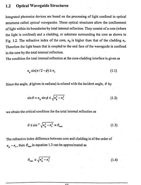
1.2
Optical Waveguide Structures
Integrated photonics devices are based on the processing of light confined in optical
structures called optical waveguides. These optical structures allow the confinement
of light within its boundaries by total internal reflection. They consist of a core (where
the light is confined) and a cladding, or substrate surrounding the core as shown in
Fig. 1.2. The refractive index of the core,
ng
is higher than that of the claddingns.
Therefore the light beam that is coupled to the end face of the waveguide is confined
in the core by the total internal reflection.
The condition for total internal reflection at the core-cladding interface is given as
(1.1)
Since the angle,
¢
(given in radians) is related with the incident angle,B
by(1.2)
we obtain the critical condition for the total internal reflection as
(1.3)
The refractive index difference between core and cladding is of the order of
n
g -n
s , thenB
max in equation 1.3 can be approximated as [image:32.546.41.528.146.787.2](}max denotes the maximwn light acceptance angle of the waveguide and is known as
the
Numerical Aperture (NA).
XL
Y z ----r~----'~--~_.::::_---~-~ x=a X
=
0z
x=-a
Cladding n,
x
n
Fig. 1.2 Basic structure and refractive index profile of optical waveguide.
An optical waveguide classification can be produced by considering the number of
dimensions in which the light is confined as shown in Table 1.1. Planar optical
waveguides confine the optical radiation in a single transverse direction. They are the
key to construct integrated optical circuits and semiconductor lasers. Considering the
refractive index distribution in the planar structure, planar waveguides can be
classified as
step-index waveguides
orgraded index waveguides.
The step-index planar waveguide is the simplest structure of light confinement, and is
formed by a uniform planar film with a constant refractive index, surrounded by two
dielectric media of lower refractive indices. The homogenous upper medium, or
upper
cladding
has a refractive index ofn
c , and the lower mediwn with refractive indexn
a•is often called
substrate.
Usually it is assumed that the refractive index of the uppercladding is less than or equal to the refractive index of the substrate,
nc
Sn
a, and inthis way we have ng
>
ns
~nco
In fact, in many cases the upper cladding is air, andtherefore
nc
=
1. If the upper and lower media are the same,ns
=nc
(equal optical constants), the structure forms a symmetrical planar waveguide. On the other hand, ifthe upper and lower media are different, it is an asymmetrical planar waveguide.
If the high index film is not homogenous, but its refractive index is depth dependent
(along the x-axis) the structure is called a
graded index planar waveguide.
Usually therefractive index is maximum at the top of the surface, and its value decreases with
depth until it reaches the value corresponding to the refractive index of the substrate.
surface modification of a substrate, whether by physical processes (ion implantation,
metal diffusion, etc.), or by chemical modification of the substrate (ionic exchange
methods).
In planar waveguides, the light confinement is restricted to a single dimension (along
the x-direction) and if the light propagates along a given direction (z-axis), the light
can spread out in a perpendicular direction (y-axis) due to diffraction. To avoid this
effect and keep the light beam well confined, it is necessary for total internal
reflection to take place not only at the upper and lower interfaces, but also at the
lateral boundaries. This confinement is attained in channel waveguides, or 2D
waveguides, in which the core region (where the optical energy is concentrated) has a
refractive index greater than any of the surrounding media.
Dimensions of light confinement
ID 2D
3D
Classification of optical waveguides
Planar waveguides Channel waveguides . Optical fibres
Photonic crystals
Table 1.1 Classification of optical waveguides according to the number of dimensions of light confinement.
Although many types of channel waveguides have been proposed, three are the most
common basic structures used. The easiest way to build a channel waveguide is to
deposit a stripe made of a high refractive index material on top of a lower refractive
index substrate. This kind of channel waveguide is called stripe waveguide, and can
be made by either depositing the stripe directly onto the substrate, or simply by
conveniently etching a previously deposited film. If the etch process is not complete
and does not reach the substrate, a channel waveguide is also produced, providing that
the thickness and height of the structure are conveniently tailored; this waveguide
[image:34.549.23.507.26.808.2]local increase of the substrate refractive index, which IS usually performed
experimentally, by diffusion methods.
Optical fibres are special type of channel waveguides, from the point of view of their
geometry and manufacturing methods as well as their applications. They have
cylindrical geometry, and are constituted by a cylindrical core of radius
a
andrefractive index ng , surrounded by a cladding of slightly lower refractive index ns.
Optical fibres are a best choice when low loss and high transmission bandwidth is
required in long-distance optical communications.
Structures also exist that confine light in the three dimensions. These constitute a very
special case of optical waveguides: since the radiation is confined in all directions, it
cannot propagate. Therefore, these structures in fact form light traps, and are often
called photonic crystals. The light confinement in this case obviously cannot be based
on total internal reflection; instead, photonic crystals are fabricated by means of
tri-dimensional periodical structures, in which the light confinement is based on Bragg
reflection. Photonic crystals have very interesting properties, and their use in several
devices and applications have been proposed, such as miniaturised lasers with
virtually no threshold power, waveguide bends with very small curvature radii and
dimensions, or narrow-band filters [2].
The slab waveguide is the simplest and most basic type of optical waveguide. It can
support a finite number of guided modes, which are associated with an infinite
number of unguided radiation modes. The boundary value problem can be formulated
using Maxwell's equations taking into account the boundary condition at interfaces to
solve for such modes. The guided modes ofthe slab waveguide can be extracted using
the approximation that is valid for short wavelength of light known as "geometrical or
ray optics".
Let's consider the cladding guide interface and a light ray, A, as shown in Fig. 1.3
incident at an angle 81 , between the light field normal and the normal to the interface.
ng sinO,
=
-ns sinO (1.5)
where 0 is the exit angle of the refracted wave AB.
From using Snell's law the guide cladding interface can also be expressed as
nc
sinO- = - - (1.6)
where O2 is the angle of the refracted ray BC, with the normal to the guide cladding
interface.
Since ng
>
nc, an incident ray is reflected into the guided region, following the path AB and when () <Be,
the total reflection conditions are not met at the guide-claddinginterface, therefore the ray is reflected to the cladding region. Similarly when the
incident angle () > Oe. the total reflection occurs and the light ray will be following the
pathBD.
When the incident angle () < Os. at the guide substrate interface, then the light ray may
refract back in to the substrate through which the light escapes from the structure
(substrate radiation modes).
Cladding
c
Core
t
ng
Substrate
When 0 is large enough total internal reflection occurs in both interfaces. This leads
to the light in the guide to be trapped and confined and propagates in a zigzag pattern
along the z direction. These are hence referred to as the guided modes.
These guided modes can be described as Transverse Electric (TE) or Transverse
Magnetic (TM) modes. For the TE mode, the electric fields are perpendicular to the
direction of the propagation. On the other hand, for TM mode the magnetic fields are
perpendicular to the direction of the propagation.
The waves travel with a wave vector kng usually in the direction of the wave where
the absolute value k is,
k
=
2:r=
(J)A
c (1.7)k is termed as the wavenumber, A, (J) and c are the free-space wavelength, angular
frequency and velocity of light in the vacuum, respectively. The mode propagation
constant,
fl,
and the phase velocity, vp , of the light wave can be expressed as [3]P
=.!!!....=kn
v sinOg
p
(1.8)
The condition for all the multiple reflected waves to add in phase is that the total
phase change experienced by the plane wave for it to travel one round trip, up and
down across the guide should equal
2m1t,
where integer,m,
is the mode order. Thephase change for the plane wave to cross the thickness, t, of the guide twice, up and
down, is
2kn
gcosO.
Furthermore, the wave suffers a phase shift of-2¢s,
on the totalreflection at the guide-substrate boundary and phase shifts
-2¢e.
due to the totalreflection at the guide-cladding interface. The above relationship yields the
self-consistency condition for the guided mode in a planar slab optical waveguide as
The above equation is also tenned as the eigenvalue or transcendental equation. By employing the Fresnel fonnulae for each polarisation [3], the phase shifts
¢s
and¢e,
for the TE waves can be expressed as
rn
2 sin2 0 _n
2V g c
tan
¢
=...!-~---C ng cosO
and in case ofthe TM waves,
(1. lOa)
(1. lOb)
(1.1la)
(1.IIb)
Similarly, expressions can also be calculated for the guide-substrate interface, by substituting the refractive index of the cladding
ne.
with the refractive index of thesubstrate,
ns.
1.3
Analysis of Optical Waveguide Structures
waveguide structures, it becomes necessary to invoke a more rigorous formalism,
based on the electromagnetic theory of the light. Therefore, implementing the
Maxwell's equations to the electromagnetic fields in a given structure, which defines
the waveguide, can solve the problem; the solutions for the fields will correspond to
the propagation modes.
There have been various analysis methods suggested for solving the optical
waveguide problems. These methods can be classified into two broad categories as
(a) Analytical approximation solution techniques
(b) Numerical solution techniques
An exact treatment of the modal characterisation in 2D waveguide is not possible, even in the simplest case of a symmetrical rectangular waveguide. Therefore, in order
to solve this problem, some analytical approximation should be made. These
analytical approximation solutions are mostly based upon the ray approximation
method (RAM) [4] and the Wentzel, Kramers and Brillouin (WKB) method [5].
However, these analytical solution methods do not satisfy the boundary conditions,
hence not being suitable for solving and analysing more practically used
three-dimensional optical waveguides whose field are of hybrid nature.
Numerical solution techniques can be classified into two groups, the domain
techniques and the boundary techniques. For the domain solution technique
(differential technique) the whole domain of the optical waveguide structure is
considered, while with the boundary technique (integral technique) only the boundary
or discontinuity regions are considered. The domain solution technique includes the
finite element method (FEM), finite difference method (FDM), beam propagation
method (BPM), and variational method (VM). The boundary solution technique
includes boundary element method (BEM), mode-matching method (MMM) and
1.4
Analytical Approximation Solution Techniques
Analytical approximation techniques had been widely used in the modelling of opto-electronic waveguides such as rib waveguides, tapers, buried waveguides and directional couplers. In the next sub-sections two widely used analytic methods will be explained: Marcatili's method and the effective index method. While the first one allows us to calculate the electromagnetic field in a rectangular waveguide (with a homogenous central core), with the latter we can obtain the optical modes supported by a waveguide with arbitrary geometry (in principle, but not easy), even with graded index regions (whether the core or the surroundings).
1.4.1 Marcatili's Method
This approximation method can be used to calculate the propagation constants and modal fields supported by a rectangular waveguide, whether stripe or buried, as the one shown in Fig. 1.4. This method was developed for guiding structures, with large dimensions, in which the refractive index difference between guiding and cladding materials is small, less than 5%. Under these assumptions, the field is assumed to exist only in the core waveguide region and in four neighbouring cladding regions, which are obtained by extending in tum the width and height of the waveguide to infinity.
Fig. 1.4 Geometry of a rectangular buried waveguide, which can be modelled by Marcatili's method.
If the propagation constant
p
of the mode is far from the cut-off(P
;::::
konl ), the electromagnetic field is confined mainly in the core (region I), and only a smallfraction of the energy carried by the optical mode spreads out to the surrounding
regions (regions II, III, IV and V).
[image:41.534.13.482.26.765.2]x
...
...
....
.
...
.
....
1
...•.
III
.•....•.•...•.
•
.
•
.•...•...•..
.
...•••...
•
y
a
v
I
IV
..
...
!
•
..
.
...
...•..
..
..
.•
II
•
•.••...•....•..
...
.
.
... .
b
Fig. 1.5 A waveguide geometry used for modal analysis employing
Marcatili's method (the shaded regions are not considered in this analysis).
Moreover, the fields penetrate even less in the four corners (dotted regions in the Fig.
1.5), and therefore in these regions there is little energy of the mode. However, poor
This is the argument used in Marcatali's method to completely ignore these comer regions, and thus the analysis can be greatly simplified. Therefore, Marcatili's method is only valid for rectangular waveguides having homogenous regions, and for guided modes far from cut-off condition. If one is interested in analysing a waveguide with a different geometry, this method is not useful, and it is necessary to tum to other approximate methods, such as the effective index method.
1.4.2 The Effective Index Method
The effective index method (ElM) is an approximate analysis for calculating the propagation modes of waveguides. This method was first proposed by Knox and Toulois in 1970 [8] with a view of extending the Marcatili's method. It is one of the simplest approximate methods for obtaining the modal fields and the propagation constant in channel waveguides having the arbitrary geometry and index profiles. It
consists of solving the problem in one dimension, described as the x coordinate, in such a way that the other coordinate (the y coordinate) acts as a parameter. In this way, one obtains a y-dependent effective index profile; this generated index profile is treated once again as a one-dimensional problem from which the effective index of the propagating mode is finally obtained.
However, the ElM is not accurate near the cut-off region, and the several other techniques have been reported to improve its performance. For instance, ElM has been used for a trapped image guide, where the original waveguide was replaced by an equivalent structure [9]. Then the transverse resonance at the air-dielectric interface is imposed, to include the free-space region of the structure and solve the problem in terms of the surface impedances in an approximate manner, and achieve an improved accuracy at low frequencies.
accuracy. As a result, many different variants of the ElM have been developed such as the ElM based on linear combinations of solutions [11], or the ElM with perturbation correction [10].
1.5
Numerical Solution Techniques
Numerical techniques generally require more computation than analytical techniques or expert systems, but they are very powerful analysis tools. Without making a priori assumptions about which field interactions are most significant, numerical techniques analyze the entire geometry provided as input. They calculate the solution to a problem based on afull-wave analysis.
The complex nature of modem optical devices has restricted the use of analytical methods to only simple structures such as those involving single layered slab waveguides. As a result, increasing attention has been focused upon improving existing numerical techniques and in other cases developing novel semi-analytical
methods [12,13].
The selection of appropriate numerical analysis method for analyzing the optical wave guiding structures is based upon several factors, which should be taken into consideration, and based on published reviews [14-16] these factors are:
(a) the shape of the cross-section area, whether it is convex or concave or whether it is uniform or non-uniform.
(b) whether the dominant mode or other higher order modes are required. (c) whether the numerical method can deal with more than two
homogenous dielectric layers.
(d) whether the field distribution or cut-off frequency is required or both .. (e) the accuracy of the technique in specific frequency ranges, especially
near cutoff frequencies.
(g) whether the technique generates spurious solutions and if so whether
the technique can identify and/or eliminate them.
(h) the computational efficiency and storage capabilities.
(i) whether the technique should be programmable, being able to solve a
wide range of structures, or it has to be programmed specifically for
each region of the structure separately.
G) the degree and understanding required from the user.
(k) the assumptions and limitations of the numerical approach, for
particular cases.
The commonly used numerical solution techniques will be briefly discussed in the
following subsections.
1.5.1 The Method of Lines
The method of lines (MoL) is a semi-analytical technique, which is mostly suitable
for the analysis of hybrid modes in optical waveguiding structures. Schulz and Pregla
[17] first suggested this method for the analysis of dispersion characteristics of planar
isotropic waveguides and microstrips. Most optical waveguide structures have a
geometry with multiplayer cross section. The channel waveguide, the rib waveguide,
and the strip-loaded waveguide can be seen as types of this class of optical waveguide
structures.
However, for a cross section with straight interface the method of lines [18,19] was
proven as an analysis procedure with the higher accuracy. Structures with curved
interfaces have also been modelled by the MoL previously using high number of
inhomogeneous layers with straight interfaces [19]. This technique has also been
applied to model optical waveguides with lossy inhomogeneous anisotropic media. In
this approach, the optical waveguide is enclosed inside a rectangular box with electric
or magnetic walls at the sides to satisfy the boundary conditions for the required