EFFICIENCY EVALUATION OF A DC TRANSMISSION
SYSTEM BASED ON VOLTAGE SOURCE CONVERTERS
Giddani O. A
(1), Grain. P. Adam
(2), O. Anaya-Lara
(3), K.L.Lo
(1) [email protected] , (2) [email protected], (3) [email protected]
Strathclyde University,
Electronic and Electrical Engineering Department Royal College Building
204 George Street, Glasgow G1 1XW
Keyword: Conversion losses, modular converter, neutral point clamped converter and pulse width modulation.
Abstract
The efficiency of a VSC-HVDC transmission system used to transmit wind farm power to the network is investigated. The losses associated with the operation of the VSC-HVDC system are the conversion losses (conduction and switching losses) in converters and the transmission losses due to I2R (in the converter transformers, smoothing reactors, and DC cables). An analytical method based on the average and root mean square of the semiconductors’ current is used to estimate the conversion losses in the converters. The remaining power losses are evaluated using I2R. The results obtained using the analytical method are confirmed by the measured losses obtained from simulation studies.
1 Introduction
High-Voltage DC transmission based on voltage source converters (VSC-HVDC) presents a solution for many problems face nowadays by power networks, such as, network congestions, grid re-enforcements and asynchronous connections. The use of forced-commutated switching devices and high-frequency pulse width modulation (in the order of 2kHz), result in a fast dynamic response to network disturbances. The main benefits of VSC-HVDC systems are: • Improving the AC fault ride-through capability.
• The absence of a reactive current component in the DC system allows active power transmission over long distances at reduced power losses.
• Independent control of active and reactive power.
• Can provide voltage and frequency support to the AC network.
• Active power flow is fully controlled and power reversal is achievable without the need to reverse the DC link polarity. • Black start capability
Currently, there are two established approaches for the construction of a VSC-HVDC system. The first approach uses a standard two-level converter or a neutral-point clamped converter with forced commutated devices such IGBTs. This approach imposes a high insulation requirement on the interfacing transformer due to the high dv/dt that results from switching high voltage with relatively low switching frequencies. This arrangement also requires fairly large filters at the output to attenuate the switching frequency components from the output voltage at the point of common coupling.
The second approach uses a two-switch modular multilevel converter with medium voltage devices such as 4.5kV IGBTs. This approach produces lower dv/dt (allowing the use of a transformer with standard insulation requirements) and significantly lower voltage harmonic distortion (which may eliminate the need for the AC filters). This approach requires however, a large number of switching devices and capacitors and a relatively complex modulation strategy compared to the first approach.
Both approaches result in fast dynamic performance, independent control of active and reactive power, no commutation failures during and AC fault, better fault ride-through capability, and the ability to provide damping and frequency support through active or reactive power modulation. However, both approaches produce higher conversion losses compared to the classic HVDC system based on line commutated or capacitor commutated current source converters.
Estimation of the power losses during the design stage of the VSC-HVDC is essential, because it allows the designers to optimize the overall system performance through a compromise of several design indices. It also helps in the selection of heat sinking equipment and cooling system for the converters.
This paper evaluates the efficiency of a VSC-HVDC system based on the three-level neutral point clamped (NPC) converter. The conversion (conduction and switching losses) and transmission losses (in AC and DC sides) are evaluated under various operating conditions. To this aim the data of a 3.3kV IGBT, and sinusoidal pulse width modulation (switching frequency of 2 kHz) have been employed.
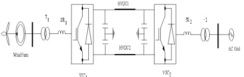
[image:2.595.41.280.302.378.2]2 Analysis of VSC-HVDC system losses
Fig. 1 shows a single line diagram of the VSC-HVDC system used in the investigation. It consists of a 700MVA wind farm based on fixed speed wind turbines. The converters VSC1 and VSC2 are modelled as NPC converters. The length of the DC cables connecting VSC1 and VSC2 is 125km.
Fig. 1. VSC HVDC system used in the investigation.
3 Conversion losses
VSC-HVDC transmission systems based on two-level and three-level NPC converters require series-connected IGBTs, therefore, the conversion losses can divided into three types as follow[1]:
1-Conduction losses:
These losses occur due to the voltage drop across the switching devices during the conduction period, and depend on the forward resistance of the device rf, the device threshold voltage
Vf0, the rms current Irms and the average current Iav .as in
equation (1).
2
cond f av f rms
P =V I +r I (1)
The device forward voltage Vf is proportional to the current i(t)
as:
V
f=
V
f0+
r i t
f( )
(2) Where (Vf0)is the forward voltage across the device at no load.2-Switching losses
The switching losses in forced-commutated devices such IGBTs are dominantly turn-on and turn-off losses. The losses in the free wheeling and clamping diodes are mainly recovery losses
during turn-off. The switching losses depend on the switching frequency and the current and voltage at each switching instant.
The most common way to evaluate the switching losses is to express the switching function as a first or second order polynomial depending on the switching characteristic of the device under consideration. However, with devices used in this paper, the first order approximation is sufficient to estimate the switching energy losses as a function of current with minimum error. Hence, the switching energy losses are expressed as:
Esw=k i1 (3)
Where k1 can be determined from the switching characteristic usually given in the manufacturers data sheet. In this paper, the two curves of switching energies (turn-on and turn-off) are added together for simplicity. With a carrier frequency more than ten times the fundamental frequency, the switching losses in Watts for three level converters can be estimated using equation (4):
1
2 1
2
sw s f
P α k i
d t
α
π
ω
=
∫
(4)3-Additional losses
These losses are produced in the gates, snubber circuits and leakage currents during the off-state and can be neglected.
4 Analytical method to calculate conversion losses in three level converters
According to equations (1) and (4) the calculation of the conduction and switching losses in any multi-level topology requires the knowledge of the rms current (Irms), the average current (Iav) flowing through each device, the device forward resistance (rf ) and the forward voltage drop of the device (Vf). The average and rms currents in any pulse width modulated converter with discontinuous current can be approximated as follow:
2 2 2
0
0 1
( ) . ( )
1
( ) . ( )
s
a a a
s s
rms a a a
s
T
T
i ia t d i t
T
i i t d i t
T
ω δ
ω δ
= ∫ =
= ∫ =
(5)
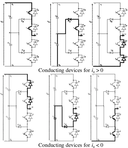
Conducting devices for ia > 0
[image:3.595.42.267.113.372.2]Conducting devices for ia < 0 Fig. 2 Power path for a 3-level converter
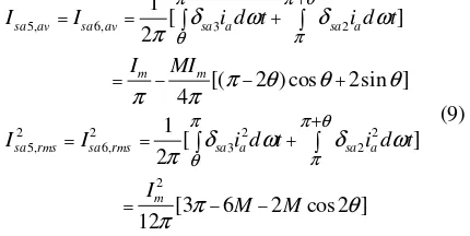
0.01 0.02 0.03 0.04
-1 -0.5 0 0.5 1 1
Carrier signals, fundamental voltage and current waveforms
0 0.01 0.02 0.03 0.040.04
0 0.5 1
Gate signal of the switch Sa1
0.01 0.02 0.03 0.040.04
0 0.5 1 1
Gate signal of the switch Sa2
0.01 0.02 0.03 0.04
0 0.5 1 1
Gate signal of the switch Sa3
0.01 0.02 0 .03 0.04 0.050.05
0 0.5 1
[image:3.595.327.530.120.203.2]Gate signal of the switch Sa4
Fig. 3: Carriers, current, voltage and gate signals waveforms.
If the load current in phase A is expressed byia
( )
t =Imsin(
ω θt−)
, the normalized phase voltage issin
a
v =M ωt and the duty cycle for the switches (S1-S4) are defined as:
1
2
3 1 4 2
sin 0
0 2 1 0
1+ sin 2
1 1
sa
sa
sa sa sa sa
M t t
t
t
M t t
ω ω π
δ
π ω π
ω π δ
ω π ω π
δ δ δ δ
≤ ≤ ⎧ =⎨ ≤ ≤ ⎩ ≤ ≤ ⎧ =⎨ ≤ ≤ ⎩ = − = − (6)
Then, the average and root mean square currents in the IGBTs are calculated as follows:
1, 4, 1
2
2 2 2
1, 4, 1
2, 3, 2
1
[( ) cos sin ]
2 4
1
[3 4cos cos 2 ]
2 12 1 [ ] 2 [4 co 4 m
sa av sa av sa a
m
sa av sa av sa a
sa av sa av a sa a
m
MI
I I i d
MI
I I i d
I I i d t i d t
I M π θ π θ
π π θ
π θ
δ ω π θ θ θ
π π
δ ω θ θ
π π
ω δ ω
π θ π = = = − + = = = + + = = + = + + ∫ ∫ ∫ ∫
2 2 2 2
2, 3, 2
2
s sin ]
1
[ ]
2
[3( ) 4 cos cos 2 ] 12
sa rms sa rms a sa a
m
M
I I i d t i d t
I
M M M
π π θ
π θ
θ θ
ω δ ω
π
π θ θ
π − = = + = − + − + ∫ ∫ (7)
And the average and root mean square currents in the freewheeling diodes are:
1, 1
4, 3, 2, 1,
2
2 2
1, 1
2 2 2 2
4, 3, 2, 1,
0
0 1
[ cos sin ]
2 4
1
[3 4 cos cos 2 ]
2 4
m
Da av sa a
Da av Da av Da av Da av
m
Da av sa a
Da rms Da rms Da rms Da rms
MI
I i d
I I I I
MI
I i d
I I I I
θ
θ
δ ω θ θ θ
π π
δ ω θ θ
The average and root mean square currents in the clamping diodes are:
5, 6, 3 2
2 2 2 2
5, 6, 3 2
2
1
[ ]
2
[( 2 ) cos 2sin ]
4 1
[ ]
2
[3 6 2 cos 2 ]
12
sa av sa av sa a sa a m m
sa rms sa rms sa a sa a
m
I I i d t i d t
I MI
I I i d t i d t
I
M M
π π θ
π θ
π π θ
π θ
δ ω δ ω
π
π θ θ θ
π π
δ ω δ ω
π π θ π + = = + = − − + + = = + = − − ∫ ∫ ∫ ∫ (9)
The currents given in (7), (8), and (9) are used to calculate the conduction losses of three-level converters according to equation (1). Therefore, the total conduction losses are:
cond condIGBTs condAnti diode condClampdiode
P
=
P
+
P
−+
P
(10).
According to equation (4) the calculation of switching losses in any multi-level topology requires the knowledge of the maximum load current value (Im), the switching frequency
( )f and the switching resistance of the device ( )k1 . For a
three-level NPC converter, the switching losses in the IGBTs Sa1 and Sa2 are:
1, 4, 1
1
2, 3, 1
1
sin( )
2
[1 cos ] 2
sin( )
2
[1 cos ]
2
s sa sw sa sw m
s m
s
sa sw sa sw m s m
f
P I k I t d t
k f I
f
P I k I t d t
k f I
π θ
π θ π
ω θ ω
π
θ
π
ω θ ω
π
θ
π
= = − = + + − − ∫ = = ∫ = (11)The switching losses associated with free wheeling devices are:
1
1 1
4 3 2 1
1
2 2
s s m
Da ,sw m
Da ,sw Da ,sw Da ,sw Da ,sw
f k f I
P k I sin( t )d t [ cos ]
P P P P
π
θ ω θ ω θ
π π = − = − = = = ∫ 1 5 1 6 5 2
s s m
Da ,sw m
Da ,sw Da ,sw
f k f I
P k I sin( t )d t
P P
π θ
θ ω θ ω
π π + = − = = ∫ (12)
Hence, the total switching losses of three-level NPC converter are:
P
sw=
P
swIGBTs+
P
swAnti diode−+
P
swClampdiode (13)5 Transmission losses
Transmission losses are:
• The losses that occur in the converter transformer (copper and iron losses) and the copper losses in the AC smoothing reactor.
• The copper losses in the DC cable
In this paper, the copper losses in the interfacing reactors and transformers are calculated using 2
3rirms, where r is the resistance
of the interfacing reactor or transformer. The iron loss in the interfacing transformer due to B f2 2and B f2 1 6. is taken as 20 percent of the copper losses. This is due to the existence of the switching frequency components and their sidebands in the converter output voltage and current. The copper losses in the DC line connecting the two converter stations is calculated using 2 2
dc dc
r I , where rdc is the DC resistance of the cable and Idc
is the current magnitude in the DC cable.
6 Efficiency evaluations
As the power losses vary with the operating point, the power losses of the VSC-HVDC system under investigation is calculated in three different operating points. Regarding conversion losses, the switches of the NPC converter must withstand half of the total DC link voltage, 150kV. With 30 percent redundancy, the number of series connected 3.3kV IGBTs needed to withstand 150kV is 60. The parameters used are:
Number of series IGBT=60 IGBT forward resistance=2.5mΩ IGBT threshold voltage VT=1.5V
Freewheeling diode forward resistance=1.8mΩ Freewheeling diode forward voltage=1.2V
The clamped diodes data are assumed the same as freewheeling diodes.
Switching energy due to turn-on and turn-off losses is expressed as: E=ki where k=215μJ/A
DC cable resistance rdc=15.9mΩ/km DC cable length =150km
Transformer AC resistance=0.25Ω/phase Interfacing reactor resistance=0.05Ω/phase
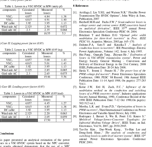
[image:4.595.53.268.145.253.2]observed that the maximum power loss conversion is obtained at 0.95 lagging (2.86% of the transmitted power).
[image:5.595.51.575.158.663.2](A) Case I: Unity power factor
Table 1. Losses in a VSC-HVDC in MW (unity pf) components Calculated
losses
Measured losses
%
VSC1 4.857 4.84 1.38 VSC2 4.815 4.91 1.40
DC cable 3.92 3.95 1.13
Wind side AC 2.325 2.50 0.072
Gird side AC 2.3 2.35 0.068
18.55 5.3
(B) Case II: Lagging power factor (0.95)
Table 2. Losses in a VSC-HVDC in MW (0.95 leg) components Calculated
losses
Measured losses
%
VSC1 4.857 5.00 1.43 VSC2 4.815 5.01 1.43
DC cable 3.92 3.95 1.13
Wind side AC 2.325 2.85 0.085
Gird side AC 2.3 2.65 0.075
19.46 5.56
(C) Case III: Leading power factor (0.95)
Table 3. Losses in a VSC-HVDC in MW (0.95 lead) components Calculated
losses
Measured losses
%
VSC1 4.857 4.45 1.27 VSC2 4.815 4.85 1.38
DC cable 3.92 3.95 1.13
Wind side AC 2.325 2.20 0.063
Gird side AC 2.3 2.05 0.059
17.50 5
.
7 Conclusions
This paper presented an analytical estimation of the power losses in a VSC-HVDC system based on the NPC converter. The results obtained demonstrate that the use of a NPC converter reduces the conversion losses in the converter as the
effective switching frequency per device is reduced to half compared to a two-level converter. An additional benefit is the reduction of power losses in the damping elements of the passive power filters required at converter output.
8 References
[1]. Arrillaga.J, Liu Y.H.L and Watson N.R,” Flexible Power Transmission-The HVDC Options”, John Wiley & Sons, Publication, 2007
[2]. Bierhoff.M.H and Fuchs.F.W ,” Semiconductor losses in voltage source and current source IGBT converters based
on analytical derivation”, IEEE 35TH annual Power
Electronics Specialists Conference PESC 04. 2004.
[3]. Brückner T and Holmes D.G “Optimal pulse width
modulation for three-level inverters” in Proc. IEEE
PESC’03, Acapulco, Mexico, 2003,pp. 165–170.
[4]. Dahono.P.A, Sato.Y and Kataoka.T ,” Analysis of
conduction losses in inverters”, IEE Proceedings -Electric
Power Applications , Volume: 142, Issue: 4, July 1995. [5]. Hui Pang , Guangfu Tang , Zhiyuan He ,” Evaluation of
losses in VSC-HVDC transmission system”, Power and
Energy Society General Meeting - Conversion and Delivery of Electrical Energy in the 21st Century, 2008 IEEE, Publication Date: 20-24 July 2008.
[6]. Ikeda Y, Itsumi J, Funato H. ,” The power loss of the
PWM voltage-fed inverter”, Power Electronics Specialists
Conference, 1988. PESC '88 Record. 19th Annual IEEE Publication Date: 11-14 April 1988, On page(s): 277-283 Vol.1.
[7]. Kolar J.W, Ertl H, Zach, F.C. ,” Influence of the modulation method on the conduction and switching
losses of a PWM converter system”, Industry applications
Society Annual Meeting, 1990., Conference Record of the 1990 IEEE Publication Date: 7-12 Oct 1990,On page(s): 502-512 vol.1.
[8]. Mestha, L.K and Evans.P.D, ” Optimization of losses in
PWM inverters”, Third International Conference on Power
Electronics and Variable-Speed Drives; July 1988.
[9]. Rodriquez J, Bernet S, Wu B, Pontt J.O, Kouro S.”
Multilevel Voltage-Source-Converter Topologies for
Industrial Medium-Voltage Drives”, IEEE Trans. on Ind.
Electronics, Vol.54, 2007, pp. 2930-2945.