Rochester Institute of Technology
RIT Scholar Works
Theses Thesis/Dissertation Collections
2011
Development of low temperature oxidation for
crystalline silicon thin film transistor applications
Ryan RettmannFollow this and additional works at:http://scholarworks.rit.edu/theses
This Thesis is brought to you for free and open access by the Thesis/Dissertation Collections at RIT Scholar Works. It has been accepted for inclusion in Theses by an authorized administrator of RIT Scholar Works. For more information, please contactritscholarworks@rit.edu.
Recommended Citation
D
EVELOPMENT OFL
OWT
EMPERATUREO
XIDATION FORC
RYSTALLINES
ILICONT
HINF
ILMT
RANSISTORA
PPLICATIONST
ITLEP
AGEBy
Ryan D. Rettmann
A Thesis Submitted
In Partial Fulfillment
of the Requirements for the Degree of
Master of Science
in
Microelectronic Engineering
Approved by:
Prof:
Dr. Karl D. Hirschman (Thesis Advisor)
Prof:
Dr. Michael A. Jackson (Committee Member)
Prof:
Dr. Robert E. Pearson (Committee Member/Program Director)
Prof:
Dr. Sohail A. Dianat (Department Head)
DEPARTMENT OF ELECTRICAL AND MICROELECTRONIC ENGINEERING KATE GLEASON COLLEGE OF ENGINEERING
ROCHESTER INSTITUTE OF TECHNOLOGY ROCHESTER, NEW YORK
D
EVELOPMENT OFL
OWT
EMPERATUREO
XIDATION FORC
RYSTALLINES
ILICONT
HINF
ILMT
RANSISTORA
PPLICATIONSL
IBRARYR
ELEASEBy
Ryan D. Rettmann
I, Ryan D. Rettmann, hereby grant permission to the Wallace Memorial Library of the
Rochester Institute of Technology to reproduce this document in whole or in part that any
reproduction will not be for commercial use or profit.
______________________________ ______________________________
A
BSTRACTDevelopment of thin-film transistor (TFT) backplane technologies has traditionally
been limited by the substrate materials used; amorphous (a-Si) or polycrystalline (p-Si)
silicon on glass. These materials have lower carrier mobility as compared to traditional
crystalline silicon CMOS technologies, resulting in performance limitations. In addition,
thermal oxidation is not a viable option for two reasons: oxidation on non-crystalline
silicon is non-uniform, and the temperature limitations of the glass, 600 °C, prevents any
appreciable SiO2 growth. This constrains the potential for a high-quality Si-SiO2 interface
necessary for aggressive scaling.
Corning Incorporated has developed a new Silicon-on-Glass (SiOG) substrate
material addressing some of these limitations [1-2]. The crystalline silicon layer allows
for high carrier mobility and a uniform surface for thermal oxidation; however the glass
substrate remains incompatible with process temperatures above 600°C for traditional
oxidation processes.
Development of a fluorine-assisted thermal oxidation process enabling substantially
higher growth rates is explored. Both NF3 and Ar/F2 additives have been shown to
provide significant enhancement in growth rate, resulting in 10’s of nanometers of oxide
at temperatures compatible with the SiOG substrate. The oxidation process has been
optimized for applications such as a sacrificial layer for ion implantation screening, or a
T
ABLE OFC
ONTENTSTitle Page ... i
Library Release ... ii
Abstract ... iii
Table of Contents ... iv
List Of Figures ... 6
List Of Tables ... 9
Acknowledgements ... 10
Chapter 1 - Introduction ... 11
1.1 Introduction and Motivation ... 11
1.2 Partnership with Corning Incorporated ... 12
1.3 Focus of this Study ... 13
Chapter 2 – Dielectrics, SiO2 and the MOS Structure ... 14
2.1 Dielectric Behavior ... 14
2.2 The MOS Structure ... 14
2.3 Charge within MOS Dielectrics ... 17
Interface Trapped Charge (Qit) ... 17
Fixed Charge (Qf) ... 18
Oxide Trapped Charge (Qot) ... 18
Mobile Ionic Charge (Qm) ... 19
2.4 SiO2 Films and Processing Techniques ... 19
Thermal Oxidation ... 19
LPCVD Oxide Deposition ... 23
PECVD Oxide Deposition ... 24
Chapter 3 – Low Temperature Oxidation ... 25
3.1 Previous Work ... 25
Morita, Aritome, Tsukude, and Hirose [6] ... 25
Kouvatsos, Huang, and Jaccodine [4] ... 27
Kazor, Jeynes, and Boyd [5] ... 29
Summary of Oxidation Studies ... 30
NF3 Assisted Oxidation ... 32
Ar/F2 Assisted Oxidation... 34
3.3 Investigation on Fluorinated Oxidation Parameters ... 36
Screening Experiment ... 37
Parametric Dependence Experiment ... 40
3.4 Silicon Thinning Process ... 44
Chapter 4 – Low Temperature CMOS TFT Fabrication... 47
4.1 Introduction ... 47
4.2 Process Flow... 47
4.3 Device Operation ... 49
Inversion Mode NFET ... 50
Accumulation Mode PFET... 51
Chapter 5 – Electrical Results ... 53
5.1 Introduction ... 53
5.2 Aluminum Capacitors ... 53
5.3 Integrated Capacitors ... 55
Lot MR ... 55
5.4 Thin-Film and bulk Transistors ... 57
Lot MR ... 57
Lot 28 – Gate Dielectrics on SiOG... 58
Chapter 6 – Materials Analysis ... 69
6.1 Introduction ... 69
6.2 Spectroscopic Ellipsometry ... 69
6.3 Secondary Ion Mass Spectroscopy (SIMS) ... 73
Chapter 7 – Conclusion ... 76
7.1 Introduction ... 76
7.2 Low Temperature Fluorinated Oxidation ... 76
7.3 Fluorinated Oxide Gate Dielectrics ... 77
7.4 Final Remarks ... 77
References ... 78
Appendix A – Fabrication Details ... 81
L
ISTO
FF
IGURESFigure 1: Diagram of typical liquid crystal display (LCD) pixel. TFTs are used as pixel drivers to activate or deactivate given color filters. [3] ... 11
Figure 2: 1-D MOS structure and band diagram of an ideal p-type silicon MOS structure under flatband conditions. ... 15
Figure 3: Inversion charge as a function of applied electrode voltage. [17] ... 16
Figure 4: Oxide charges and their location within the MOS system. Note the separation of the charges is for clarity, each type could be expected to be distributed evenly. ... 16
Figure 5: a.) Band diagram of structure in Figure 2 with positive oxide charge. b.) New flat-band bias with oxide charge present. ... 17
Figure 6: a.) Side view of Si-SiO2 interface. The Si and O atoms are represented by light
and dark spheres, respectively. Each arrow points to a row of unbounded oxygen atoms. Notice the substantial voids above each bridge bond. b.) Energy of each atom vs. its z coordinate. The solid line is the local energy per atom, averaged over 20 simulated configurations [22]. ... 18
Figure 7: "Deal Triangle" showing the combined Qit and Qf values and their relationships to oxidation growth and anneal conditions on a (111) wafer [19]. ... 20
Figure 8: Oxidation rate modeling for 1000° C dry oxidation. ... 22 Figure 9: Thin oxidation regime as identified by Deal and Grove, for 700 °C. Extremely fast oxidation occurs in dry oxidation for very thin oxides. ... 23
Figure 10: Oxidation rate curves as a function of fluorine concentration, from Morita. Cold-walled, NF3 oxidation [6]. ... 26
Figure 11: Histogram of dielectric breakdown, demonstrated by Morita et al [6]. ... 26
Figure 12: Oxide thickness versus time at 800 C, reported by Kouvatsos. Hot-walled, NF3 oxidation [4]. ... 28
Figure 13: Stress data by ambient NF3 concentration, reported by Kouvatsos [4]. ... 28
Figure 14: Oxide thickness grown for various conditions in 30 min. Reported by Kazor. Cold-walled, Ar/F2 oxidation [5]. ... 29
Figure 15: ID-VG characteristics VDS=0.1 V (bottom curve), VDS=1 V (middle curve) and
VDS=5 V (top curve), 800 °C gate oxidation, 30 ppm NF3 for 50% of the time, heavy
hydrogen plasma passivation, W/L= 10, L= 5microns. Fluorinated oxide TFTs as reported by Kouvatsos [9]. ... 31
Figure 16 Diagram of first revision oxidation chamber. ... 32
Figure 18: Oxide thicknesses demonstrated using Ar/F2 catalyst. All runs performed for
1 hour soak at temperature. ... 34
Figure 19: C-V Measurements of initial Ar/F2 enhanced growth rate oxides. Note that for the substrate and oxide thickness used, an ideal threshold of -0.75 V would be expected. ... 36
Figure 20: Comparison of annealed and unannealed fluorinated oxide C-V measurements. Shift in curve center indicates a shift in the magnitude of oxide charge present in the MOS system. ... 36
Figure 21: Screening experiment on SOI wafer samples. 2 center point replicates were used. ... 37
Figure 22: a.) Oxide etched leverage plot. b.) Oxide grown leverage plot. Note that the majority of oxide is typically etched away during processing. ... 39
Figure 23: a.) Remaining oxide dependence on soak temperature. b.) Oxide dependence on fluorine flow... 39
Figure 24: Oxide thickness (tox) dependence on all three experimental factors. Note the general quadratic dependence on fluorine flow. ... 41
Figure 25: Oxide etched (tet) dependence on all three experimental factors. Statistically, all three dependencies are linear. ... 43
Figure 26: Time trial for 600 °C, 30 sccm Ar/F2 flow process. ... 43
Figure 27: Lot RGM-SOI samples post active etch. Center region is silicon active mesa. a.) Silicon thinned to 130 nm using fluorinated oxidation process. b.) Standard 200 nm SiOG thickness... 45
Figure 28: Fluorinated oxidation thinning SiOG surface roughness. a.) Native SiOG surface roughness, Ra = 6.0 nm. b.) Thinned SiOG roughness, Ra = 5.8 nm. ... 46
Figure 30: Inversion mode NFET device schematic. ... 51
Figure 31: Accumulation mode PFET device schematic. ... 51
Figure 32: C-V measurements of various post-oxidation anneal treatments. ... 55
Figure 33: Lot MR integrated capacitor C-V data. Fluorinated oxide samples exhibited breakdown past 2 V. ... 56
Figure 34: Layout of RingGate transistor. Device geometry creates a self-isolated channel region. ... 57
Figure 35: ID-VG results of Lot MR 16 x 96 PFETs. ... 58
Figure 36: Lot 28-D1 12x24 transistor. Significant Si mesa erosion following gate etch. ... 59
Figure 37: Lot 28-D2 gate etch process. ... 60
Figure 38: Lot 28-D9 12x24 transistor following chemical etch of molybdenum. ... 60
oxide on SOI. b.) Wafer D7, PECVD TEOS oxide on SOI. c.) Wafer D4, PECVD TEOS on SiOG. d.) Wafer D8, fluorinated thermal oxide on SiOG. e.) Wafer D9, fluorinated thermal oxide on SiOG. Data filtered for clarity. A tests performed at VD=|0.1| V on
W=24 µm, L=12µm devices. ... 61
Figure 40: Threshold voltage statistics for Lot 28. a.) NFET devices. b.) PFET devices. A tests performed at VD=|0.1| V on W=24 µm, L=12µm devices. ... 63
Figure 41: Subthreshold Slope statistics for Lot 28. a.) NFET devices. b.) PFET Devices. A tests performed at VD=|0.1| V on W=24 µm, L=12µm devices. ... 64
Figure 42: Comparison of ID-VG data from lot 28 SOI samples. a.) Logarithmic scale. b.) Linear scale. A tests performed at VD=|0.1| V on W=24 µm, L=12µm devices. ... 65
Figure 43: ID-VG data from Lot 28 SOI samples a.) D6, fluorinated oxide. b.) D7, TEOS oxide. Lighter colors indicate VD=|2.5| V, dark colors VD=|0.1| V. All tests performed on
W=24 µm, L=12µm devices. ... 65
Figure 44: Threshold voltage statistics for Lot 28 SOI NFET devices under saturation. Tests performed at VD=|2.5| V. ... 66
Figure 45: Threshold voltage statistics for Lot 28 SOI PFET devices under saturation. Tests performed at VD=|2.5| V. ... 67
Figure 46: Subthreshold slope statistics for Lot 28 SOI NFET devices under saturation. Tests performed at VD=|2.5| V. ... 67
Figure 47: Subthreshold slope statistics for Lot 28 SOI PFET devices under saturation. Tests performed at VD=|2.5| V. ... 68
Figure 48: Ellipsometric measurement results of fluorinated oxide process at 600 °C for 2 hour with an Ar/F2 flow of 30 sccm, comparing a.) unannealed sample CV-1, and b.)
sample with a 10 minute O2, 20 minute N2, anneal at 525 °C immediately following
oxidation, CV-2, and c.) a 10 minute O2, 50 minute N2, anneal at 525 °C, CV-3. ... 70
Figure 49: Optical constants for various thermally grown oxides, and reference index values. ... 71
Figure 50: Fit study of sample CV-3. Film thickness is swept and Cauchy parameters are allowed to float to achieve minimum mean square error (MSE). R2 value indicates linear correlation between A0 and thickness. ... 73
Figure 51: SIMS Profile of sample CV-1, fluorinated oxide sample with no post-soak anneal. ... 74
Figure 52: SIMS Profile of sample CV-2, fluorinated oxide sample with a 10 minute O2,
20 minute N2, anneal at 525 °C immediately following oxidation. ... 74
Figure 53: SIMS Profile of sample CV-3, fluorinated oxide sample with a 10 minute O2, 50 minute N2, anneal at 525 °C immediately following oxidation. ... 75
L
ISTO
FT
ABLESTable 1: Summarized fluorinated oxidation work. ... 30
Table 2: Device characteristics of polysilicon TFTs are reported by Kouvatsos [9]. ... 31
Table 3: NF3 oxidation C-V and optical measurement results. ... 34
Table 4: Process window parameter experiment. 2 center points were performed for a total of 38 runs. ... 40
Table 5: Parameter estimates for oxide remaining on wafer surface (tox). ... 40
Table 6: Parameter estimates for oxide etched during process (tet). ... 40
Table 7: Wafer fabrication and treatment combination. Thermal oxide treatments were all performed using an optimized 600 °C fluorinated oxidation process documented in Chapter 3. Codes following wafer number on SiOG samples are wafer scribe numbers, as processed at Corning Incorporated. ... 49
Table 8: Dielectric measurements of fluorinated oxide treatments. ... 54
Table 9: C-V and Thickness data for lot MR integrated capacitors. ... 56
Table 10: Lot MR measured device parameters. ... 58
A
CKNOWLEDGEMENTSFirst, I would like to thank the Team Eagle research group for their support and
assistance in processing and data analysis; Patricia Meller, Andrew McCabe, Chris Shea,
and Brian Silkey. Special thanks to Robert Manley, along with Germain Fenger, Robert
Saxer, and Eric Woodard, for laying the foundation on which a substantial amount of this
work is based. Along with Team Eagle, special thanks to our collaborators at Corning
Incorporated; Dr. J. Gregory Couillard and Dr. Carlo Kosik Williams.
Additionally, I would like to thank the entire Microelectronic Engineering faculty at
RIT, who have built the program and provided the education that made this work
possible. Specifically, special thanks to my committee members; Dr. Robert Pearson and
Dr. Michael Jackson, who’s guidance and wisdom was critical. Thanks also to my
Advisor, Dr. Karl Hirschman, for his constant support and assistance throughout this
project. And thanks to Sara Widlund, for constantly navigating the RIT bureaucracy on
behalf of myself and all students.
I also need to thank the staff of the Semiconductor and Microsystems Fabrication
Laboratory, for significant assistance training and for maintaining the tools and facilities
necessary to carry out this work. Special thanks to David Yackoff and John Nash for
construction and maintenance of the fluorinated oxidation process chamber.
Finally, thank you to Dan and Dawn Kirchoff, for everything great parents do for
C
HAPTER1
-
I
NTRODUCTION1.1 Introduction and Motivation
In the display industry, thin film transistors (TFT) are used as backplane pixel drivers
for flat panel display monitors, as depicted in Figure 1. These TFTs are fabricated on
glass substrates using a deposited thin film semiconductor, often amorphous (a-Si) silicon
or polysilicon (p-Si). Fabrication of TFT backplane devices is significantly different than
bulk silicon devices due to thermal constraints imposed by the strain point of the
substrate glass and the unique electrical isolation of the thin-film semiconductor. This
introduces a number of limitations on process techniques typically available to CMOS
fabrication. In addition, the economics of the display industry places strong pressure to
drive down panel manufacturing cost, limiting the allowed complexity of fabrication
processes. Due to the above constraints, dopant activation becomes challenging, device
complexity is limited, and thermal oxidation is unavailable at any significant thickness.
As such, traditionally inferior oxide deposition techniques, specifically PECVD, are used
[image:12.612.225.425.518.677.2]in lieu of a thermally grown oxide.
In traditional silicon CMOS processing, the benefits of a thermally grown oxide for
use in sacrificial layers and gate dielectrics are well known. Work exploring the quality
benefits of trace amounts of chlorine in gate oxidation, as well as a slightly increased
growth rate, has long been demonstrated. Some exploration of the potential of small
concentrations of fluorine to enhance oxidation rates has been performed, however at
limited depth and only on bulk silicon samples [4-8]. Several groups have shown a
substantial growth rate enhancement, however little study has been done on device
structures with fluorinated oxides. Complex relationships among process parameters,
including temperature, fluorine concentration, and chamber design have been observed.
Further understanding of the enhancement mechanism and other reactions is desirable.
Polysilicon TFTs have been fabricated using low temperature oxidation as a
demonstrated proof of concept [9]. To date, c-Si TFTs using a low temperature
fluorinated oxide gate dielectric have not been reported.
1.2 Partnership with Corning Incorporated
Flat panel display is an area where research activities are rapidly advancing the
technology. The process development and characterization work required for this project
match exceedingly well with the teaching and research interests of the Electrical and
Microelectronic Engineering Department. Corning is specifically interested in
investigating the potential for high performance TFTs fabricated on the SiOG substrates.
As part of this effort, process techniques not typically seen in display manufacturing are
considered including ion implantation and reduction lithography [10-13]. In this work,
1.3 Focus of this Study
The primary focus of this work is to investigate and optimize a low temperature
thermal oxidation process for use in c-Si TFT fabrication. Mapping the process space to
understand the interactions of fluorine concentration, temperature, and oxidation time is
presented. Insight into an etch mechanism that coexists due to the presence of fluorine
during low temperature oxidation (not previously documented) is provided. In addition,
dielectric parameters are extracted using electrical characterization of fabricated devices
and direct materials characterization techniques are performed on fluorinated oxide
samples. Delivery of recommended process settings and process parameter dependencies
C
HAPTER2
–
D
IELECTRICS,
S
IO
2 AND THEMOS
S
TRUCTURE2.1 Dielectric Behavior
A dielectric is an insulating material that exhibits an electric dipole structure; either
the molecular or atomic components exhibit electrical polarization [14]. This
polarization behavior results in a shift of the permittivity of the material, a measure of the
resistance of a material to the formation of an electric field. The ratio of a materials
permittivity to the permittivity of free space is known as the relatively permittivity, ϵr, or dielectric constant, κ. By employing materials with higher dielectric constants, increased
capacitance can be achieved at equal capacitor geometries by equation 1, where ϵ0 is the permittivity of free space, 8.854x10⁻¹² F/cm, C is capacitance, A is the area of the parallel
plates, and l is the distance between the plates [15].
(1)
2.2 The MOS Structure
A diagram of the MOS structure along with its corresponding energy band diagram is
shown in Figure 2. A thin dielectric layer separates a semiconductor substrate and a
metal electrode material. In a p-type semiconductor, as positive voltage is applied to the
metal electrode an electric field forms that pushes holes from the semiconductor surface.
This results in the creation of a depletion region; only fixed negatively charged acceptor
ions contribute charge. At sufficient applied voltage, thermally generated electrons will
is an approximation; it is often defined as the extrapolation of the linear portion of the
inversion charge vs. applied voltage curve to the x-axis, shown as VT0 in Figure 3 [17]. Inversion charge is directly proportional to the magnitude of drive current a MOS
field effect transistor is capable of providing, which is a key predictor of circuit
performance and switching frequency. Increased gate control is accomplished by an
increase in MOS capacitance, which enables device scaling [18].
As the formation of the both the depletion region and inversion channel are dependent
on the balance of charge in the system, any charge present in the oxide region or at the
oxide-semiconductor interface will influence the electrical characteristics of the device.
Silicon based MOS scaling has traditionally depended on increased gate control of the
underlying semiconductor [18]. Charge present within the oxide requires additional gate
voltage in order to balance the system. Thus, a minimization of this charge is desirable
for consistent device performance. Oxide charge is broken down into four varieties, as
shown in Figure 4 [19-21].
a. b.
Figure 2: 1-D MOS structure and band diagram of an ideal p-type silicon MOS structure under flatband conditions.
EC
Ei Efp EV EF
Figure 3: Inversion charge as a function of applied electrode voltage. [17]
Figure 4: Oxide charges and their location within the MOS system. Note the separation of the charges is for clarity, each type could be expected to be distributed evenly.
Presence of charge within the dielectric results in the modified band structures shown
in Figure 5. The additional positive charge acts as a built in positive bias on the
semiconductor, causing the onset of depletion and inversion to occur at a lower gate bias
than in the ideal case. Note that a negative oxide charge would cause the opposite shift,
however this is not often observed. Metal
SiO2
SixOy
Si
a. b.
Figure 5: a.) Band diagram of structure in Figure 2 with positive oxide charge. b.) New flat-band bias with oxide charge present.
2.3 Charge within MOS Dielectrics
Interface Trapped Charge (Qit)
Oxide interface charge results from structural differences in the interface between
crystalline silicon and amorphous silicon dioxide. It has been demonstrated that this type
of charge has been found to have a lower practical limit of ~1x1010 cm-2.
Exact origins of this charge are not yet fully understood. However, computer
simulations have been employed to further understand the nature of the Si-SiO2 interface.
Figure 6 shows a graphical representation of the simulated results. A transition between
the average bond length of c-Si and amorphous SiO2 results in lines of unbonded bridging
oxygen atoms. These bridging oxygen atoms contributed to the resultant interface
Figure 6: a.) Side view of Si-SiO2 interface. The Si and O atoms are represented by light and dark spheres, respectively. Each arrow points to a row of unbounded oxygen atoms. Notice the substantial voids above each bridge bond. b.) Energy of each atom vs. its z coordinate. The solid line is the local energy per atom, averaged over 20 simulated configurations [22].
Fixed Charge (Qf)
Fixed charge results from a transition region within the SiO2 layer a few nanometers
from the interface. This transition region is generally silicon rich, and allows some
resultant free bonding states. As the film growth is stopped, some residual unbounded
silicon atoms are left in this region resulting in fixed positive charge centers. Careful
treatment of the oxide following growth can drive this and interface charge together
down to a lower limit of ~9x1010 cm-2. Application of a post-metallization anneal on
devices employing aluminum interconnects has been shown to reduce this charge,
coupled with Qit to levels of 3~5x1010 cm-2.
Oxide Trapped Charge (Qot)
Other trap charges within the bulk of the oxide can be either positive or negative.
These charge centers can be caused by radiation, hot carrier injection, imperfections in
the amorphous oxide film, or other impurities that are immobile. As this type of charge
charge. However, excessive trapped charge can assist with tunneling mechanisms and
degrade the oxide quality, both from a leakage and reliability standpoint.
Mobile Ionic Charge (Qm)
If metal ions such as sodium or potassium are introduced into the oxide, a memory
effect on the apparent threshold of the device can be introduced. As such ions are
relatively mobile within the oxide, and can be moved with bias or temperature. Their
location relative to the semiconductor can have varying impact on their apparent
influence. Careful processing methods, most importantly proper cleaning prior to oxide
growth or deposition, can mitigate this issue [20].
2.4 SiO
2Films and Processing Techniques
For a variety of reasons including ease of process integration, temperature stability,
and most importantly interface quality, silicon dioxide has become a dominant dielectric
used in the semiconductor industry [16, 23]. A variety of oxide deposition techniques are
utilized during typical CMOS processing. During initial stages of a given process run,
thermal oxidation is generally preferred. As thermal oxidation consumes a portion of the
silicon during growth, the resulting silicon surface is pristine after oxide removal. In
addition, the resultant oxide interface quality tends to be highest with a thermally grown
oxide; thus it is often used as the gate dielectric where this attribute is critical.
Thermal Oxidation
A bare silicon wafer when exposed to an oxidizing ambient such as O2 or H2O at high
temperatures will readily grow an oxide film. This method tends to be the easiest process
processing only requires an atmospheric furnace and various gas supplies, equipment and
processing cost is relatively low.
Deal et al. laid out much of the theoretical framework for the processing of high
quality thermal oxides in 1967 [19]. Most significantly, as discussed above, the
framework describing the four main types of oxide charge are described. In addition, the
techniques for mitigating Qf and Qit through inert anneals or high temperature growth were demonstrated. As dry oxidation temperature was increased, lower charge was
observed within the oxide. However, a lower temperature oxide can be annealed in an
inert ambient to bring oxide charge levels to the high-temperature limit. This is
diagrammed in Figure 7.
Figure 7: "Deal Triangle" showing the combined Qit and Qf values and their relationships
to oxidation growth and anneal conditions on a (111) wafer [19].
Generally, dry oxidation using an O2 ambient produces higher quality oxides than a
have demonstrated the lowest values of interface charges. This is explained by the (100)
family of planes containing the lowest planar density in the silicon crystal lattice.
Thermal oxidation is commonly described using the Deal-Grove model [24]. This
model assumes that the oxidation reaction occurs at the oxide-silicon interface, opposed
to the oxide-ambient interface. The oxidant, either O2 or H2O, diffuses through the oxide
layer, and there forms new oxide by reacting with the silicon substrate. Given the above,
the oxidation rate will be governed by both the concentration of available oxidant at the
oxide-silicon interface and the reaction rate of the process. The concentration at the
interface can be described using Henry’s law to determine the maximum concentration of
oxidant that can be diffused into the oxide (gas-phase solubility), and Fick’s law to
determine the diffusion rate of the oxidant.
While a thin layer of oxide is present, typically during the initial stages of oxidation,
the growth rate is limited by the reaction rate of the silicon and the oxidant. Thus, the
growth rate is linear with time, until a thickness of oxide is reached, at which point the
mass transport of the oxidizing species becomes the dominant limiting factor. During
this regime, the growth rate becomes parabolic, slowing as the oxide layer thickens. The
process can be described by the differential Equation 2.
(2)
Where xo is the oxide film thickness, k is the partial pressure of the oxidant, C* is the equilibrium concentration of the oxidant in the oxide, N1 is the number of oxidant molecules incorporated into a unit volume of the oxide layer, h is the gas-phase transport
Setting the boundary condition of x0 = xi at t = 0 allows the solutions shown in Equations 3 and 4. These describe the oxide thickness at time t with a given correction
factor τ (an equivalent time required for any oxide that may be present before the
oxidation run). B/A is known as the linear rate constant, and has typical units of µm/hr.
B is the parabolic rate constant, and has typical units of µm2/hr. B and A are groupings of
constants from Equation 2.
(3)
(4)
Figure 8 shows the predicted oxide thickness values for a dry oxidation performed at
1000° C. Note that through most of the oxidation, a mix of the two oxidation modes dominates the final oxide thickness. Only at very short or very long oxidation times is
the process predominantly a single mechanism.
It is important to note that Deal et al. identified a region under dry oxidation prior to
the onset of the linear regime of oxidation wherein growth rate is nearly exponential, as
shown in Figure 9. This regime has been explored, and a number of mechanisms have
been proposed to explain this, however a general consensus has not been reached [25-28].
Figure 9: Thin oxidation regime as identified by Deal and Grove, for 700 °C. Extremely fast oxidation occurs in dry oxidation for very thin oxides.
LPCVD Oxide Deposition
LPCVD deposition chambers can be advantageous in that they can produce high
purity, conformal films in large batch processes. As the process is a deposition rather
than a growth, mass-transfer through the oxide film is no longer required. Thus, the
deposition rate of LPCVD oxides can be linear over significantly greater thicknesses, and
can be much higher than thermal oxidation. Large batches of wafers can then be
processed uniformly be the reaction-rate limited process. Typical operating temperatures
Deposition techniques also carry the advantage of not being a growth process; no
silicon is consumed by depositing the film. This removes one possible integration
concern arising from thermal oxidation.
PECVD Oxide Deposition
In plasma assisted CVD processes, a low temperature plasma discharge is used to
sustain chemical reactions for deposition. This allows for even lower processing
temperature than LPCVD based systems, and/or higher deposition rates. However, the
use of excited gas as a reactant species introduces many challenges in process integration.
As the reaction is generally more complex, non-stoichiometric films can be formed,
although this is not always desirable. Impurities from incidental species can also be
introduced through the plasma process. As an ionized and excited gas is present within
the plasma, charge can be introduced into the final oxide if not tuned carefully. Oxide
precursors frequently used are silane (SiH4) and oxygen (O2) mixtures, and tetraethyl
orthosilicate (Si(OC2H5)4.
PECVD, as a low temperature process that can be expanded uniformly to large
surfaces, is the predominant method of oxide deposition in the display industry. Note
that charge levels in the oxide and at the Si/SiO2 interface are typically higher in PECVD
C
HAPTER3
–
L
OWT
EMPERATUREO
XIDATION3.1 Previous Work
This section describes work performed on the investigation of fluorinated oxidation
of silicon by various groups. The experiments range over various ambient and
temperature conditions, method of fluorine introduction, and oxidation chamber design.
A combination of materials characterization and electrical measurement techniques were
used to investigate the resulting dielectric properties and interface quality.
Morita, Aritome, Tsukude, and Hirose [6]
Morita et al. first demonstrated the increased oxidation rate potential of a fluorine
additive. Figure 10 shows the thicknesses achieved. A cold-walled oxidation furnace
was employed, and halogen lamps were used to irradiate the wafer surface to provide the
thermal energy necessary for oxidation. A strong dependence on fluorine concentration
within the gas ambient is observed. A peak oxide thickness location occurs at each
temperature/fluorine-flow combination. This was concluded to be driven by the
decomposition rate of NF3; a high temperature being necessary to generate enough free F
Figure 10: Oxidation rate curves as a function of fluorine concentration, from Morita. Cold-walled, NF3 oxidation [6].
Figure 11: Histogram of dielectric breakdown, demonstrated by Morita et al [6].
Morita also first introduced a proposed etch mechanism; resulting in thinner oxides at
higher fluorine concentration, although no attempt was made to quantify it. It should be
noted that at 600 °C, essentially no oxidation (beyond a native oxide) would be expected.
[image:27.612.221.426.269.549.2]has yet to be explained. When integrated into a MOS structure, any positive charge
within the dielectric is expected to cause a negative shift in threshold voltage of the
device, or a positive shift for negative charge. As a negative ion, fluorine incorporation
would be expected to cause a positive shift in MOS threshold voltage; however the
fluorinated oxide yielded a shift of -1.4 V suggesting some other charge mechanism was
operative. Finally, a sampling of dielectric breakdown measurements was performed.
Traditional bulk SiO2 is known to have a dielectric breakdown of approximately
10 MV/cm. Figure 11 shows the results of the measured fluorinated oxide. It is likely
that these numbers are not compensated for I-R voltage loss due to series resistance, thus
yielding breakdown fields higher than the theoretical maximum.
Kouvatsos, Huang, and Jaccodine [4]
A group at Lehigh University has reported several times on various aspects of
fluorinated oxidation. In contrast to Morita, a hot-walled oxidation tube employing more
conventional resistive heating elements was used. Kouvatsos et al. focused more on
stress and film density, and reported a markedly different thickness dependence on
fluorine concentration. As can be seen in Figure 12, a peak oxide thickness is not
observed, showing only a point of growth saturation. Film stress analysis was carried
using a wafer curvature measurement apparatus. Wafer curvature is related to film stress
by Equation 6; where E and ν are the Young’s modulus and Poisson ratio of the Si
substrate, tf and ts are the thicknesses of the film and the substrate, and Rf and R0 are the final and initial radii of curvature.
Figure 12: Oxide thickness versus time at 800 C, reported by Kouvatsos. Hot-walled, NF3 oxidation [4].
A significant reduction in film stress was observed in fluorinated oxides as compared
to dry oxidation, as shown in Figure 13. This was thought to be caused by fluorine
decreasing the viscosity of the oxide film. As fluorine is incorporated into the amorphous
structure, it bonds with Si, preventing the formation of rigid -Si-O-Si- rings. This in turn
increases the self-diffusion rate of oxidant species through the film. Additionally, the
authors conclude that reduced oxide stress would correlate with reduced oxide density;
however this has only been demonstrated with traditional oxidation methods, and may
[image:29.612.225.420.75.221.2]not be valid for fluorinated oxides.
Kazor, Jeynes, and Boyd [5]
Kazor et al. employed a gas mixture of 5% F2 in Argon gas. Using this source,
enhanced growth rates at significantly lower temperatures than had been previously
reported were obtained, shown in Figure 14. A dependence of peak growth rate on NF3
concentration is observed, similar to Morita’s results. In addition to reporting results
from a much lower temperature regime, Kazor also identifies several favorable reactions
that lend credibility to previously proposed fluorine-oxide kinetics. At the silicon-oxide
interface an exothermal reaction, shown in equation 7, can take place along with the
expected low-temperature oxidation reaction between silicon and the oxidant species.
(7)
This reaction creates additional available Si bonding sites, potentially increasing the
oxidation reaction rate at the interface. A concurrent reaction, shown in equation 8, could
result in both increased oxidant diffusivity (by altering the film microstructure) and the
oxide etch mechanism.
(8)
Summary of Oxidation Studies
A summary of key findings from previous studies is presented in Table 1. It is
observed that the etch mechanism is only evident on cold-walled oxidation chamber
designs. Additionally, diatomic fluorine appears to be a substantially more effective
enhancement catalyst than NF3, which was also noted by Kazor. This could potentially
be driven by nitrogen reacting and incorporating into the oxide structure, limiting oxidant
diffusion. In addition, the higher dissociation energy of the NF3 molecule could be
limiting the enhancement mechanism at lower temperatures [5].
Table 1: Summarized fluorinated oxidation work.
F Source Chamber Design
Proposed Mechanism
Etch Temp
Range
Morita NF3 Cold-wall Reaction rate,
diffusivity Yes 600-800
Kouvatsos NF3 Hot-wall diffusivity No 800-1000
Kazor F2 Cold-wall
Reaction rate,
diffusivity Yes 400-550
Polysilicon TFTs Fabricated using Fluorinated Oxides
Kouvatsos et al. fabricated polysilicon TFTs using a fluorinated oxide in 1996 [9].
Figure 15 shows the transistor characteristics for a transistor made at a thermal budget of
800 °C. A variety of fluorinated oxide treatment devices are fabricated, with the lowest thermal budget being 650 °C. These devices exhibited a minimum subthreshold slope of 0.7 V/decade. Table 2 shows summarized devices characteristics of the various gate
oxide treatments.
Figure 15: ID-VG characteristics VDS=0.1 V (bottom curve), VDS=1 V (middle curve) and VDS=5 V (top curve), 800 °C gate oxidation, 30 ppm NF3 for 50% of the time, heavy hydrogen plasma passivation, W/L= 10, L= 5microns. Fluorinated oxide TFTs as reported by Kouvatsos [9].
Table 2: Device characteristics of polysilicon TFTs are reported by Kouvatsos [9].
3.2 Preliminary Study
A horizontal hot-walled furnace with an 800 °C torch was outfitted with a direct injection fluorine inlet, shown in Figure 16. Initially, an NF3 gas source with a mass flow
controller (MFC) rated at 2-8 sccm was used as the fluorine source. Oxidation rates
and diatomic fluorine (5%) was performed. All oxidations were performed using a single
wafer, with the wafer surface facing the torch; this was done due to initial screening
experiments indicating substantially less enhancement on any other wafer within the
chamber. Thus, the oxidation process developed is a single-wafer process.
Figure 16 Diagram of first revision oxidation chamber.
NF3 Assisted Oxidation
Initial work performed using NF3 as the fluorine source showed marginally enhanced
oxidation rates at elevated temperatures [8]. However, the enhancement observed at the
required 600 °C was inconsistent and non-uniform. Figure 17 shows the oxidation rates
of a O2 ambient oxidation at 700 °C and 800 °C, with and without an 8 sccm NF3 flow
injected into the ambient. Roughly a factor of 2 increase in oxidation rate was shown at
Figure 17: Fluorinated oxidation rates using 8 sccm NF3.
To investigate the impact of the fluorinated oxidation process on the dielectric
properties and charge levels of the oxide, aluminum electrode capacitors were fabricated
using oxide films grown under various treatment combinations. Sample 1-2 Ω-cm n-type wafers were oxidized, aluminum was deposited and patterned, and a 450 °C sinter was applied in an N2/H2 ambient. Table 3 shows thickness and measured oxide charge levels
of the various treatments. A consistent decrease in the magnitude of charge measured in
the oxide was observed on samples grown using the NF3 catalyst. The physical cause of
this change is not well understood. It has been surmised that fluorine atoms are bonding
to un-bonded silicon or oxygen sites, or it could simply be that the fluorine ions are
Table 3: NF3 oxidation C-V and optical measurement results.
Optical Oxide Thickness [nm]
Electrical Oxide Thickness [nm]
Oxide Charge [cm-2]
800 °C, 2 hour, 1600 ppm NF3 20.1 19.4 4.51x10¹⁰
800 °C, 4 hour, dry oxidation 19.3 20.3 1.33x10¹¹
700 °C, 4 hour, 1600 ppm NF3 22.1 20.9 5.18x10¹⁰
700 °C, 12 hour, dry oxidation 23.1 22.7 1.32x10¹¹
Ar/F2 Assisted Oxidation
Due to the limited enhancement observed with NF3 used as a fluorine source, source
comprised of a mixture of 95% Ar and 5% F2 was explored following the NF3
investigation [29]. Significantly higher growth rates were observed using this catalyst.
Figure 18 shows the influence of Ar/F2 flow rate on oxide growth at 650 °C. Where
previously nearly no oxide was grown at this temperature regime, a thickness upwards of
50 nm was grown.
Figure 18: Oxide thicknesses demonstrated using Ar/F2 catalyst. All runs performed for 1 hour soak at temperature.
100 150 200 250 300 350 0 100 200 300 400 500 T h ic k n e ss ( Å )
Aluminum gate capacitors were again fabricated and C-V measurements performed.
A significant left shift of the threshold was observed, as seen in Figure 19, indicating a
substantial positive oxide charge present. This is unexpected and somewhat
counter-intuitive; fluorine, being a group 7 element, forms a negative ion, which would induce a
right shift on the C-V curve. It is possible that some molecular ion is forming within the
film, such as SiF4+. It is also possible that the fluorinated oxidation process leaves a
significant amount of fixed and interface charge in the SiO2 structure.
Upon application of a two stage anneal process, one hour in O2 following one hour in
N2, both at 525 °C, significant reduction in oxide charge can be observed. Figure 20
shows a comparison of annealed and unannealed oxides by C-V measurements.
Substantial improvement of oxide quality can be achieved with annealing and
post-metallization thermal treatment processes. The post-oxidation anneal in N2 reducing
oxide charge is consistent with expectations from oxidation theory, indicating that the
charge present in the unannealed oxide is a more traditional SiO2 related fixed or
Figure 19: C-V Measurements of initial Ar/F2 enhanced growth rate oxides. Note that for the substrate and oxide thickness used, an ideal threshold of -0.75 V would be expected.
Figure 20: Comparison of annealed and unannealed fluorinated oxide C-V measurements. Shift in curve center indicates a shift in the magnitude of oxide charge present in the MOS system.
3.3 Investigation on Fluorinated Oxidation Parameters
Previous studies have reported complex relationships between oxidation temperature
-4 -2 0 2 4
0.0 0.2 0.4 0.6 0.8 1.0
Annealed Thermal Oxide Thermal Oxide
N
o
rm
a
li
z
e
d
C
a
p
a
c
it
a
n
c
e
decreases. This effect is suspected to be an etch mechanism of the fluorine present in the
system, widely used as an etchant in both the IC and display industries. This etch rate
mechanism has been suspected to have unique dependencies on fluorine concentration
and temperature, requiring a balance of the two to maximize the resulting oxide film
thickness. All previous work reported on fluorine enhanced oxidation rates has been
reported on bulk silicon substrates.
By leveraging spectroscopic ellipsometry (SE) to measure the entire SOI stack before
and after a given oxidation step, both growth and etch of the oxide growth of a given
treatment can be measured [30].
Screening Experiment
An initial screening experiment was performed on fluorine concentration and soak
temperature. All runs were done with a 1 hour soak time. A 2x2 central composite
design with an α value of 1.414 was used. Figure 21 shows the treatment combinations used.
The ellipsometric measurement yields two direct measurement results, surface oxide
thickness (tox) and superficial silicon thickness (tsi). By measuring both these quantities before and after growth, and relating the change in silicon thickness to an assumed total
oxide grown, three responses can be obtained: total oxide grown (tg), oxide etched (tet), and the final surface oxide thickness (tox). These responses are related by equations 9 and 10. The goal of the experiment was to maximize tox while minimizing tet.
(9)
(10)
Using a 95% confidence interval, the only significant factor for etch rate and growth
rate was Ar/F2 flow. For the final oxide thickness, both temperature and Ar/F2 flow was
significant. As shown in Figure 22, a significant thickness of oxide is grown and etched
during the process. It is important to note that more than half of the superficial silicon on
a standard SiOG wafer would be consumed at the higher end fluorine flow rate in this
a. b.
Figure 22: a.) Oxide etched leverage plot. b.) Oxide grown leverage plot. Note that the majority of oxide is typically etched away during processing.
[image:40.612.121.529.70.280.2]a. b.
Figure 23: a.) Remaining oxide dependence on soak temperature. b.) Oxide dependence on fluorine flow.
The final remaining oxide thickness showed a significant and clear relationship to
both fluorine concentration and ambient temperature. Figure 23 shows the measured
results. The thickest remaining oxide, which also corresponds to the least oxide etched,
Parametric Dependence Experiment
Using the results from the initial screening experiment, a 6x2x3 full factorial
experiment was designed around fluorine flow rate, soak time, and temperature. Table 4
shows the treatment matrix of the experiment. Due to the strong dependence on fluorine
flow both in literature and the screening experiment, increased resolution was given to
this parameter.
Table 4: Process window parameter experiment. 2 center points were performed for a total of 38 runs.
Ar/F2 Flow sccm 20 25 30 35 40 45
Temperature °C 500 600
Soak Time minute 30 60 120
Full results from this experiment can be found in Appendix A. The remaining oxide
thickness was shown to be linearly dependant on temperature and soak time, with a
square dependence on fluorine flow rate. Table 5 shows the sorted parameter estimates
and t values for each of these factors.
Table 5: Parameter estimates for oxide remaining on wafer surface (tox).
The etch mechanism demonstrated a strong linear dependence on both fluorine flow
rate and soak time, and a marginal inverse dependence on oxidation temperature, as
shown in Table 6. Contrary to expectations, increased temperature actually decreased the
amount of oxide etched during the process. This mechanism is not well understood.
The measured relationships between the input factors and oxide thickness are shown
in Figure 24. A maximum film thickness of 26.7 nm was found at a treatment of 30 sccm
Ar/F2 flow, 600 °C soak temperature for a two hour soak time.
Figure 24: Oxide thickness (tox) dependence on all three experimental factors. Note the
general quadratic dependence on fluorine flow.
Results of the quantity of etched oxide are shown in Figure 25. The inverse
[image:42.612.108.543.274.606.2]hour soak time. By combining the direct relationship between tox and fluorine flow and the inverse relationship between tet and fluorine flow, an optimum process space for thin film oxidation can be explored.
Figure 26 examines the extended soak times of this process space. From this it is
clear that the final oxide thickness is a non-linear response to extending the oxidation
time. While the etch rate remains relatively constant over the full 8 hours, the growth
rate falls off quadratically.
While the mechanism of the fluorinated oxidation process remains poorly understood,
this relationship indicates a diffusion limited mechanism, similar to the parabolic regime
in the Deal and Grove oxidation model. It is possible that fluorine incorporation
increases oxidant diffusion rate through the oxide, although this alone would not explain
the enhancement, as at this temperature range even the pure dry oxidation reaction rate is
Figure 25: Oxide etched (tet) dependence on all three experimental factors. Statistically,
all three dependencies are linear.
[image:44.612.147.505.430.692.2]Empirical rate equations can be generated using a statistical analysis software
package. These are shown in Equations 11-13. It should be noted that the R2 values for
these equations are on the order of 0.7, and thus the model is only loosely predictive. A
more precise model could be generated for a given region of the process space that would
fit data more closely; however such a model would be of little utility, as the number of
fitting parameters would be significant.
(11)
(12)
(13)
3.4 Silicon Thinning Process
One potential application for fluorinated oxidation on thin film substrates is silicon
thinning. As oxidation is a growth mechanism, a thickness of silicon is consumed during
the process, and by tuning oxidation parameters characterized in Section 3.3, controlled
silicon thinning can be performed. Some initial observations into this process are
reported here.
An SiOG wafer with a starting Si thickness of 196.4 nm was exposed to a 2 hour,
600° C oxidation with an Ar/F2 flow rate of 100 sccm. This process, based on the results
gathered previously, would be expected to remove roughly 75 nm of silicon. Post
oxidation, an oxide thickness of 16.5 nm and a silicon thickness of 133 nm as measured
using SE. This sample was then processed through the standard low temperature CMOS
the glass substrate, shown in Figure 27a. A standard micrograph of the process is show
in Figure 27b for comparison. Defects appear to be present regardless of silicon
presence, and were not noted prior to active etch. It is possible that fluorine incorporated
into the glass substrate is interacting with the SF6 based active etch plasma.
aa a. b.
Figure 27: Lot RGM-SOI samples post active etch. Center region is silicon active mesa. a.) Silicon thinned to 130 nm using fluorinated oxidation process. b.) Standard 200 nm SiOG thickness.
In addition to optical micrographs a set of atomic force microscopy measurements
were taken to investigate surface roughness before and after fluorinated oxidation
thinning. After oxidation, the sample was immersed in 10:1 buffered oxide etch to
remove the grown oxide. No appreciable degradation or improvement in silicon surface
rms roughness was observed, as shown in Figure 28.
Significantly more work is needed to fully explore this application of fluorinated
oxidation at low temperatures. Silicon layer thickness uniformity and surface quality
should be measured and documented more thoroughly. Additionally process
a. b.
C
HAPTER4
–
L
OWT
EMPERATURECMOS
TFT
F
ABRICATION4.1 Introduction
As part of the research and development relationship between Corning and RIT
outlined in Section 1.2, regular TFT fabrication is carried out on SiOG substrates. This
process flow is a modification of the flow originally defined by Saxer and Manley [10].
Typically, SOI wafers are used as process control vehicles to ensure fabrication is
performed properly. Here, the ‘standard’ process flow was used with modifications to
allow for fluorinated oxidation processing during gate stack formation.
Some further deviations from standard processing were made following gate
patterning, driven by etch concerns. These details are outlined in section 5.4.
4.2 Process Flow
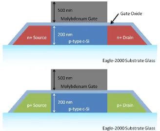
[image:48.612.160.488.419.687.2]The modified process flow first defined by Saxer and Manley was used to fabricate
TFTs on bulk Si, SOI, and SiOG samples. Using 1x1015 cm-2 p-type surface silicon SOI
and SiOG substrates, a general outline of the fabrication process is as follows. First,
silicon mesas are lithographically defined and etched. Gate oxidation and deposition
splits are performed. Molybdenum is sputter deposited to 500 nm as the gate metal
electrode, and patterned. A 60 nm screen oxide is deposited using LPCVD. Using
lithographically defined windows in photoresist to select device type, self-aligned source
and drain implants are performed, activated by a 600 °C anneal. Contact cuts are patterned and etched, and aluminum is deposited as the contact metal. The aluminum is
then patterned, and the wafers are placed in a 425 °C sinter to complete the process. Figure 29 shows the resulting n and p type TFTs. Complete listing of processing steps
can be found in Appendix A.
For bulk samples, only PFET devices were fabricated, and self-isolated devices
termed ring-gate transistors were tested. The geometry of this device is such that the
drain completely surrounds the source, negating the need for any additional isolation
techniques. This was employed for ease of integration with the above process which
would not adequately isolate devices fabricated on bulk substrates.
Wafer splits were performed at the gate oxidation step to investigate various
treatment combinations. LPCVD was included as a reference standard, as a large body of
data characterizing devices based on this oxide at RIT. Two treatments of PECVD oxide
were used, based on results generated by Fenger [31]. Finally, a sampling of thermal
Following the gate oxidation split, all devices were processed from gate metallization
on together. SiOG samples were prepared by Corning. Table 7 shows the gate oxide
treatment, substrate, and fabrication run matrix.
Table 7: Wafer fabrication and treatment combination. Thermal oxide treatments were all performed using an optimized 600 °C fluorinated oxidation process documented in Chapter 3. Codes following wafer number on SiOG samples are wafer scribe numbers, as processed at Corning Incorporated.
Fabrication Run Wafer ID Substrate Treatment
Lot MR1 D3 Bulk LPCVD – 50 nm
Lot MR1 D4 Bulk Thermal – 25 nm
Lot 28 D1 202097-BL SiOG Thermal – 10 nm
Lot 28 D2 202097-TR SiOG Thermal – 25 nm
Lot 28 D3 202098-BL SiOG Thermal – 50 nm
Lot 28 D4 202098-TR SiOG PECVD TEOS – 25 nm
Lot 28 D6 SOI Thermal – 25 nm
Lot 28 D7 SOI PECVD TEOS – 25 nm
Lot 28 D8 202100-BL SiOG Thermal – 25 nm
Lot 28 D9 202226-BL SiOG Thermal – 25 nm
4.3 Device Operation
Significant analysis of the device operation of both the NFET and PFETs fabricated
using the above process has been performed and documented [10-12, 32]. For this study,
two significant factors must be considered for interpreting device performance as related
to the quality of the gate dielectric. As p-type starting silicon is used, the NFET device
fabricated functions as a traditional inversion mode n-type TFT. However, as an
iso-type junction is formed on the p-iso-type TFTs, these devices function as accumulation mode
[image:50.612.101.547.213.439.2]as the inversion mode device, a greater dependence on gate dielectric characteristics is
expected to exist on the NFET device [33]. Both devices are fully depleted devices.
Second, as TFT device performance is dependent on the body thickness of the device,
thermal oxidation could potentially confound the influence of gate dielectric quality and
the thinning of the body of the device.
Inversion Mode NFET
Below threshold, there exists an accumulation layer of holes isolating source from the
drain preventing current flow. Once threshold is reached, an inversion layer forms below
the silicon-oxide interface, allowing current flow; as shown in Figure 30. As this
inversion layer is extremely thin compared to the body thickness, it is typically
approximated to be a sheet of zero thickness. The mobility of carriers flowing through
this inversion layer is a function of both the quality of the body semiconductor, the
coloumbic scattering resulting from body doping, and the scattering of carriers resulting
from the transverse electric field pulling carriers toward the silicon-oxide interface. It
follows that the quality of this interface will significantly impact the mobility of carriers
in the channel. Equation 5 describes an empirical model to account for this effect, where
µ0 is the bulk carrier mobility, accounting for body doping, and Θ is a fit parameter [17].
Figure 30: Inversion mode NFET device schematic.
Accumulation Mode PFET
[image:52.612.184.467.406.647.2]Figure 31 shows the device operation of the accumulation mode PFET. Below
threshold, an inversion layer is generated preventing current flow through the device [32,
34]. As threshold is reached, holes accumulate in the body region, creating a path for
current flow. As accumulated holes will be less localized to the surface than the
inversion layer, the transverse field, and thus the silicon-oxide interface, is expected to
have less influence on device operation than on the NFET device.
An extensive study has been done by R. Manley on the impact of topside and
C
HAPTER5
–
E
LECTRICALR
ESULTS5.1 Introduction
Several devices were fabricated as part of the complete study. Aluminum capacitors
were fabricated on bulk n-type substrates using optimized fluorinated oxidation
processes. Two lot process runs were performed in which molybdenum gate integrated
capacitors and both thin-film and bulk transistors were fabricated. The first lot
fabricated, Lot MR, included two n-type bulk wafers on which inversion mode PMOS
transistors were fabricated. A split at gate oxidation was performed, with one sample
receiving a standard 50 nm LPCVD oxide and another receiving a fluorinated oxidation
yielding a 28 nm thermal oxide. Lot 28 included seven total device wafers, with the
treatment combinations listed in Table 7. In addition to thin film transistors, each wafer
included a series of thin-film capacitors across the surface of the wafer.
All current-voltage measurements were carried out using an Agilent 4156B
semiconductor parameter analyzer, either using manual probes for discrete testing or in
conjunction with an ElectroGlass 2001X automated probing station for cross-wafer
testing.
5.2 Aluminum Capacitors
Aluminum was evaporated and patterned on the wafer surface, and a 1 hour H2/N2
anneal at 425 °C was applied to all samples following metal patterning. Capacitance-voltage measurements were then taken using an MDC probing station with chuck
Again, counter-intuitive charge presence noted in section 4.2 was observed. When no
anneal is applied following fluorinated oxidation, a significant amount of positive charge
is measured within the oxide. After anneal, this charge appears to be reduced. There is
also a significant amount of cross-wafer non-uniformity, as evident in Figure 32.
Assuming a dielectric constant of 3.84, electrical thickness measurements were taken
on the aluminum capacitor samples. Table 8 shows the summarized results, along with
corresponding anneal treatments. Sample CV-1 received no post-oxidation anneal. CV-2
received a 30 minute 525 °C anneal, 10 minutes of O2 ambient, 20 minutes of N2. CV-3
received a 60 minute 525 °C anneal, 10 minutes of O2 ambient, 50 minutes of N2.
Also note decreasing oxide charge measured as anneal time is increased. Sample
CV-3 shows low enough oxide charge to be comparable with the established LPCVD oxide
used in standard SiOG CMOS processing. This anneal treatment was used on both Lot
MR and Lot 28 integrated device fabrication thermal gate oxides.
Table 8: Dielectric measurements of fluorinated oxide treatments.
Sample Anneal Time
[min]
Optical Thickness [nm]
Electrical
thickness [nm] Qox [cm
-2]
CV-1 n/a 25.1 24.9 1.9 · 1012
CV-2 30 23.4 21.2 3.4 · 1011
Figure 32: C-V measurements of various post-oxidation anneal treatments.
5.3 Integrated Capacitors
Lot MR
In addition to stand-alone aluminum dot capacitors, C-V measurements were taken on
integrated capacitors with molybdenum gates fabricated in conjunction with lot MR TFT
devices. A subset of these measurements is shown in Figure 33. A significant delta in
maximum capacitance is likely driven, to a first order, by the delta in oxide thickness.
The fluorinated oxide samples exhibited dielectric breakdown at ~ 2.5 V, or 1 MV/cm.
This is extremely low, and is significantly lower than the TFT dielectric breakdown or
~4 MV/cm documented in section 5.4. This is thought to be related to the relative area of
TFTs and integrated capacitors; the increased area of the capacitors allows a greater
Charge levels for both oxides were low, as shown in Table 9. As observed with the
aluminum capacitors, the effective oxide thickness of the fluorinated oxide appears
greater than the measured oxide thickness.
[image:57.612.148.541.162.417.2]Figure 33: Lot MR integrated capacitor C-V data. Fluorinated oxide samples exhibited breakdown past 2 V.
Table 9: C-V and Thickness data for lot MR integrated capacitors.
Wafer Gate Oxide Optical Thickness
[nm]
Electrical
Thickness [nm] Qox [cm -2
]
D3 Fluorinated
Oxide 21.1 23.8 2.5 · 10
10
D4 LPCVD 49.8 53.1 2.1 · 1010
D3: Fluorinated Oxide


![Figure 13: Stress data by ambient NF3 concentration, reported by Kouvatsos [4].](https://thumb-us.123doks.com/thumbv2/123dok_us/51781.4726/29.612.225.420.75.221/figure-stress-data-ambient-nf-concentration-reported-kouvatsos.webp)