Abstract—High-order wide-output (HOWO) impedance source converters (ISCs) have been presented for ac inverter applications that require voltage step-up ability. With intrinsic passive impedance networks as energy sources, these converters are able to achieve voltage boosting with either polarity, leading to improved dc-link voltage utilization compared with the conventional two-level converter. However, HOWO-ISCs suffer from transfer functions giving low bandwidth, a penalty of increased passive devices and right-half-plane zeros, which result in lower order distortion of the ac output power. In this paper, a modified plug-in repetitive control scheme is presented for HOWO-ISCs with accurate reference tracking (hence low distortion), fast dynamic response, and enhanced robustness. By using zero-phase-shift finite impulse response filters in both the internal model of the repetitive controller and its compensation network, the proposed method achieves zero steady-state error and an extended closed-loop bandwidth. For HOWO-ISC cases, this method outperforms conventional proportional-integral (PI) control, which has considerable steady-state error. It also eliminates the need of parallel loops for several frequencies when proportional resonant control or orthogonal transformation based PI schemes are used to remove lower order distortion. The design process and performance analysis of the proposed repetitive control strategy are based on a novel three-phase HOWO-ISC configuration with a reduced number of switches. Simulation and experimental results confirm the feasibility and effectiveness of the proposed control approach.
Index Terms—Impedance source converter; dc-ac conversion; low distortion; power converter modeling; digital repetitive control, zero-phase-shift filter.
I. INTRODUCTION
ith an increasing demand for interconnecting multiple dc distributed energy resources (DERs) such as photovoltaic (PV), fuel cell and battery storage devices with the traditional energy infrastructures, a power inverter stage becomes necessary to convert the dc energy source into an ac waveform [1-3].
Since a single DER unit usually has a low output voltage, matured schemes employ many units to create a high dc-link voltage for transferring the power through a conventional
Manuscript received on May 03, 2016; revised on August 21, 2016; accepted on September 26, 2016..
Y. Wang, A. Darwish, D. Holliday, B. Williams are with Department of Electronics and Electrical Engineering, University of Strathclyde, Glasgow, G1 1XW, UK. (e-mail: yachao.wang@strath.ac.uk, ahmed.mohamed-darwish-badawy@strath.ac.uk, derrick.holliday@eee.strath.ac.uk, barry.williams@ eee.strath.ac.uk).
central inverter, which has only voltage step-down characteristics [4, 5]. However, this method does not guarantee an optimal operation point for each DER unit [6].
To enable distributive access to low dc voltage DERs for improved energy utilization, power inverters with output voltage boosting ability are required [7]. With such motivation, a range of impedance source converter (ISC) topologies have been introduced in the recent literature [8-16], among which, the Ćuk, sepic, Z-source (SZS) and semi-quasi-Z-source (SQZS) topologies all consists of two inductors and two capacitors as in their dc-dc switched mode classified by Tymerski [17]. By using an impedance network as virtual energy source, these converters achieve improved dc-link voltage utilization and terminal current profiles. However, the higher number of passive elements increases the order of converter transfer function; thus, complicating the modeling process. Specifically, high-order wide-output (HOWO) ISC topologies have non-minimum phase characteristics with extra phase lagging effect, which imposes limitation on the control design for achieving high loop-gain (low tracking error) and sufficient stability margin. Hence, a reliable control strategy with accurate reference tracking ability is demanded for ISCs, which enables them to precisely execute the system level command for power flow regulation in an interconnected energy network, such as maximum power point tracking.
In an ac system, conventional instantaneous value based proportional-integral (PI) control cannot achieve zero steady-state tracking error. Thus, PI control in the synchronous reference frame (SRF) using frequency decoupling, is employed [11] in the three-phase SQZS converter. However, to cancel the resonant peak in its transfer function, the active bandwidth needs to be reduced to a low level which weakens the dynamic performance. Also, parallel control loops for each frequency are adopted to guarantee output power quality, which leads to undesirable interaction between the different loops due to the frequency decoupled model approximation. Similarly, to save on mathematical transformations, parallel proportional resonant (PR) control loops are applied to the Ćuk type three-phase inverter in [12] to achieve sufficient harmonic rejection. Since each PR control loop targets only a specific frequency component, multiple control loops are needed; where the loops may interact. This complicates the controller and its efficiency. Nonlinear schemes such as sliding-mode control have been employed in differential mode sepic and Ćuk converters [13, 14]. The target variable usually cannot be directly controlled; so a proper sliding surface, combining several state variables, has to be selected.
High-Plug-in Repetitive Control Strategy for High-Order
Wide Output Range Impedance Source Converters
Yachao Wang,
Student Member
,
IEEE
, Ahmed Darwish,
Derrick Holliday and Barry W. Williams
2 pass filters are required to derive the transient signal of the
control input in a time-variant ac system. Also, the sliding surface coefficient is influenced by parameter mismatches and load variations, which affects the practical performance.
Repetitive control, based on the internal model principle, is able to attenuate periodic disturbances, and has been adopted in power electronic converter applications [18-23]. In [20], plug-in repetitive control is directly adopted for the SPWM two-level inverter in an uninterruptable power supply (UPS), to ensure a low distortion, robust output voltage. In [21], parallel plug-in repetitive control with reduced data memory is used in a bridgeless rectifier topology. The modular multilevel converter (MMC) circulating current can also be eliminated by repetitive control, as in [22, 23]. However, unlike the mentioned topologies, HOWO-ISC transfer functions usually have right-half-plane (RHP) zeros, time-variant zero-pole locations, and high resonant peaks. These factors impose higher demand on the design of digital filter and compensator parameters over that for a lower order converter model.
This paper presents a generic design of a digital plug-in repetitive control strategy for a family of HOWO ISCs with emphasis on the analysis of the zero-phase-shift (ZPS) filter and compensation network to achieve an extended closed loop bandwidth (improved dynamic response) and minimized reference tracking error. In the proposed strategy, an inner PI control loop and a zero-phase-shift (ZPS) finite impulse response (FIR) compensator are employed to stabilize the converter model plant with improved error convergence speed. Another ZPS low-pass FIR filter is incorporated in the internal model feedback path of the repetitive controller to attenuate the high frequency gain. In this manner, the robustness of the overall system is guaranteed. The paper is organized as follows: section II gives a brief review of representative HOWO ISC topologies with their potential configurations for multi-phase ac applications. Then the design process of the proposed control strategy is described using a selected case study with a novel three-phase SQZS converter configuration having a reduced number of switches. Simulation and
experimental verification form section IV, and finally, outcomes and observations are highlighted in section V.
II. REVIEWOFHOWO-ISCTOPOLOGIES Four representative HOWO-ISC topologies are reviewed to give an understanding of their technical merits and operational challenges, which are critical for control design. Based on inverter mode operation for a solar energy harvesting system, the characteristics of these topologies in three-phase configurations are analyzed.
A. Operation principles of the HOWO-ISC topologies
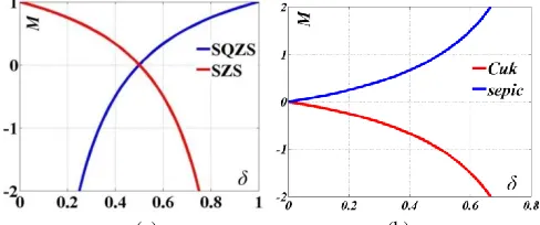
Table 1 summarizes the schematics and main operational features of four representative HOWO-ISC bidirectional topologies, including the semi-Z-source (SZS), semi-quasi-Z-source (SQZS), Ćuk and sepic converters, in which each have two inductors and two capacitors [10-14]. In Table 1, where δ is the duty cycle of S1 (complementally, δ′=1-δ is the duty cycle of S2) for all candidates, their voltage transfer ratio M can be derived from the inductor steady-state volt-second balance principle. In Fig. 1(a), the SZS and SQZS converters afford bi-polarity voltage output; while, as shown in Fig. 1(b), the Ćuk and sepic converters have unipolar voltage gains. The extended output voltage range of these HOWO-ISCs create increased voltage and current stresses on the power switches, which are a function of the duty cycle as in Table 1 . Also, in [12, 24], the Ćuk and sepic converters can be derived into their high frequency isolated versions by using coupled inductors.
[image:2.612.48.568.57.279.2](a) (b)
[image:2.612.316.560.600.702.2]Fig. 1. Steady-state voltage transfer ratio of: (a) SZS and SQZS and (b) Ćuk and sepic converters.
Table 1. Schematics, voltage transfer ratio, and voltage and current stresses of power switches of four ISCs.
SZS SQZS Ćuk sepic
Topology
Voltage transfer ratio
' 2 1
M 2 1
M M '
'
M
Voltage
stress dc
'
V
dc
V
'
dc
V
'
dc
V
Current
stress o
'
I
I
o
o
'I
'
o
I
i/p and o/p current
discontinuous/
discontinuous discontinuous/continuous continuous/continuous continuous/discontinuous
High frequency
isolated version
The ISC topologies have been developed mainly to improve the AC side voltage magnitude (thus, dc-link voltage utilization) in the conventional half-bridge inverter [10-14]. Using the basic converter modules in Table 1, both two-leg (four-switch) and three-leg (six-switch) configurations can be employed for three-phase dc-ac applications, as in Table 2.
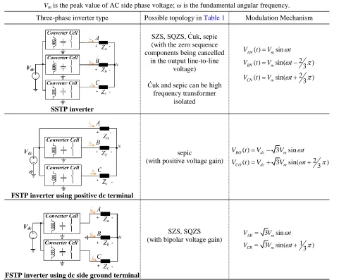
[image:3.612.69.560.319.716.2]As with typical six-switch three-phase (SSTP) inverters, and all the topologies in Table 1, any dc components and zero sequence harmonics cancel in the output line-to-line voltages [11, 12]. The four-switch three-phase (FSTP) inverter with two buck converters and the mid-point of dc-link capacitor feeding the three-phase output [25], reduces the device and passive component count. Similarly, for the ISC topologies, the sepic converter can be configured as a FSTP inverter by using the dc source positive terminal, since it has a positive step up/down gain [13]. This scheme inherits a dc offset common mode voltage between its dc ground and AC neutral point. To suppress such a dc common mode voltage, as shown in Table 2, the SZS and SQZS converters with bipolar voltage gain are developed as FSTP inverters in this paper, among which the SQZS solution is selected as the case study for generic control design interpretation. The Ćuk converter
cannot be used as an FSTP inverter due to its negative voltage gain (its output cannot be within the rail bounds).
B. Constraints of HOWO-ISCs
Although improved dc-link utilization can be achieved by ISC schemes, the passive components of their impedance network introduce a high number of poles and zeros (including RHP zeros) into their transfer functions. This leads to a low closed-loop bandwidth, high steady-state error, and considerable lower order harmonic distortion for the HOWO-ISCs when conventional PI control is employed.
As analyzed in [11], the SSTP SQZS converter inherits 2nd order harmonic distortion in its output voltage, which requires two parallel control loops to manage the fundamental and 2nd order harmonic simultaneously. However, in the FSTP or single-phase applications, the lower order distortion is distributed continuously in the baseband including 3rd order harmonic components; hence this parallel loop method becomes complex and inefficient.
To address this limitation, a generic repetitive control strategy applicable for all HOWO-ISC configurations is developed in the next section. Specifically, the islanded mode SQZS FSTP inverter is used as the illustrative case study due
Table 2. Configurations for three-phase inverters using basic units in Table 1.
Vm is the peak value of AC side phase voltage; ω is the fundamental angular frequency. Three-phase inverter type Possible topology in Table 1 Modulation Mechanism
SSTP inverter
SZS, SQZS, Ćuk, sepic (with the zero sequence components being cancelled
in the output line-to-line voltage)
Ćuk and sepic can be high frequency transformer
isolated
( ) sin
2
( ) sin( )
3 2
( ) sin( )
3
AN m
BN m
CN m
V t V t
V t V t
V t V t
FSTP inverter using positive dc terminal
sepic
(with positive voltage gain)
( ) 3 sin
2
( ) 3 sin( )
3
BO dc m
CO dc m
V t V V t
V t V V t
FSTP inverter using dc side ground terminal
SZS, SQZS (with bipolar voltage gain)
3 sin 1
3 sin( )
3
AB m
CB m
V V t
4 to its control design complexities, with the following factors:
1) The islanded mode SQZS converter has a higher order transfer function than in a grid-connected mode due to the pole caused by the output capacitor and
2) Unlike the SSTP configuration with zero-sequence component cancellation, the FSTP converter requires phase independent control for distortion immunity over the full baseband range, including the zero-sequence harmonics.
III. PLUG-INREPETITIVECONTROLLERFORSQZS FSTPINVERTER
A. FSTP SQZS Inverter
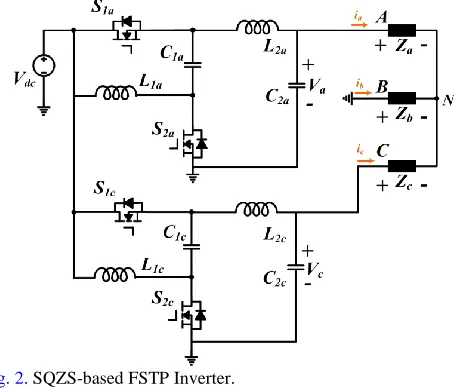
[image:4.612.314.534.126.222.2]Based on Table 1 and Table 2, the FSTP SQZS inverter can be depicted as in Fig. 2, where two SQZS converter output terminals and the dc negative reference are connected to a three-phase balance load. In this arrangement, the total device and passive component count is reduced. If Vdc is the dc input voltage, Vm is the peak value of the desired output phase voltage, and ω is angular fundamental frequency; in order to achieve the output voltage as in (1), the modulation references for the two SQZS converters are expressed by(2).
Fig. 2. SQZS-based FSTP Inverter.
From Fig. 2, the two SQZS converter output voltages in the FSTP configuration are equal to the line-to-line voltages VAB and VCB, respectively. With the voltage gain of the SQZS topology in Fig. 1(a), its maximum ac output voltage magnitude is Vdc; thus, in an FSTP arrangement, the peak phase voltage Vm is 0.5774Vdc, which is higher than ½Vdc in the conventional three-phase two-level inverter (using six switches, without triplen injection). Also, compared to the sepic based FSTP inverter [13], this scheme has a pure sinusoidal ac common mode voltage (no dc component) between its ac side neutral point and the dc-link negative terminal. This eases the insulation design for an interfacing transformer in a grounded system.
2 3
2 3
( ) sin
( ) sin( )
( ) sin( )
AN m
BN m
CN m
V t V t
V t V t
V t V t
(1) 1 6 1 2( ) 3 sin( )
( ) 3 sin( )
a m
c m
V t V t
V t V t
(2)
In contrast to SSTP inverters, where the zero sequence components cannot propagate onto the line-to-line voltage, their FSTP counterparts require each converter output voltage to be a purely fundamental component. This requires the control strategy of ISC based single-phase or FSTP configurations to have sufficient harmonic rejection over all baseband frequencies.
B. Modeling of the SQZS converter
Fig. 3. SQZS converter topology.
The SQZS converter topology is redrawn in Fig. 3, where L1 (with parasitic resistance r1) and C1 form the impedance source network; L2 (with parasitic resistance r2) and C2 form the second order output filtering stage; Vdc is the input voltage and R is the load impedance in islanded mode. The two switches operate in a complementary manner with the duty cycle of S1 as the control input, which can be decoupled into a steady-state value δ plus its small perturbation ∆δ in classical small signal dynamic analysis.
Then linearizing, the generic small-signal transfer function G(s) of the SQZS converter is (3), where ∆vo represents the small voltage increment caused by the duty cycle perturbation ∆δ around the steady-state value.
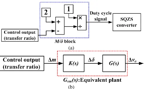
Similarly, applying this perturbing and linearization method to the steady-state equation of the voltage transfer ratio M and duty cycle δ in (4) (see Table 1), the dynamic relationship between ∆m and ∆δ is as in (5). Therefore, to view the voltage transfer ratio as the controller output signal, the equivalent plant of the SQZS converter for control design can be rearranged as in (6) and Fig. 4. Then the dc steady-state gain of the plant transfer function Gvm(s) (s=0) becomes independent of duty cycle variation (neglecting inductor parasitic resistance).
2
0 1 2
2 3 4
0 1 2 3 4
0 1
1 1 1 1
2 1 1
2
0 1 2 1
2 2
1 2 2 2 2 1 1 1 1 2
2
2 2 1 2 2 1 1 1 2
1 ( ) ( ) ( ) ( 1) ( 1)
( ) (2 1)
( ) ( 1) ( ) ( )
( ) (2 1) ( )
o dc
v s V A A s A s G s
s B B s B s B s B s
A R M r
A C Rr M L A C L R
B R r r r
B C Rr L C Rr L C r R r B C R L L C L R C L R r
C L
2 1 1 2 1 2
3 1 2 1 2 1 2 2 1 1 1 2 4 1 2 1 2
r C C Rr r
B C C RL r C C RL r C L L B C C L L R (3) 1 2 M
(4)
2
( )
( )
( )
s
K s
m s
(5)
2
( )
( )
( )
( )
( )
( )
o vmv s
G
s
K s G s
G s
m s
[image:4.612.56.283.305.499.2](a)
(b)
Fig. 4. Relationship between voltage transfer ratio and duty cycle in SQZS converter: (a) the signal transformation and (b) small-signal equivalent plant for controller design.
In quasi-steady-state analysis of the SQZS inverter, the voltage transfer ratio M should be modulated as a pure sinusoidal waveform as in (7), where Am is the ratio of the converter ac side voltage magnitude (line-to-line voltage for the FSTP inverter) over the dc-link voltage. Then, from (4), the duty cycle can be estimated by (8) when ignoring the internal inertia of the SQZS converter.
( ) msin
M t A
t(7)
1
1
( )
2
( )
2
msin
t
M t
A
t
(8)
The passive element parameters of the SQZS converter are usually determined by the voltage and current peak ripple constraints, as discussed in [10, 12, 13]. With these principles, the FSTP SQZS inverter specification for this study is shown in Table 3.
[image:5.612.325.549.41.373.2]In Table 3, with the shown dc-link and ac side line-to-line voltages, Am = 0.8; hence, the duty cycle of each SQZS converter module varies approximately between 0.36 and 0.83, based on (8). Then, by substituting the parameters in Table 3 and varying the steady-state duty cycle δ, a family of Bode plots and pole-zero plots for the transfer function Gvm(s) result as in Fig. 5.
From Fig. 5(b), when the duty cycle is less than ½, RHP zeros emerge, leading to non-minimal phase system performance with significant phase delay, as shown by the phase-frequency Bode plots in Fig. 5(a). Thus, a phase-leading compensation network is required to increase the phase margin and improve the dynamic response [26]. Also, in the amplitude-frequency Bode plots of Fig. 5(a), the resonant peak increases with increasing duty cycle.
Table 3. Rated Values for the FSTP SQZS Inverter.
Power rating P 2 kW
Per phase load R 2.5 Ω
Input dc voltage Vdc 125 V
AC line-to-line peak voltage √3𝑉𝑚 100 V
Inductor L1 and L2 0.5 mH
Capacitor C1 and C2 10 µF
Switching frequency
(sampling frequency) fs 30 kHz
Fundamental frequency fo 50 Hz
(a)
(b)
Fig. 5. SQZS inverter characteristics with duty cycle variation: (a) Bode plots of Gvm(s) and(b) pole-zero map.
This time-varying performance with duty cycle is in-line with the topologically asymmetrical operation of the SQZS inverter (also other ISCs) for generating bipolar voltage. For example, in the SQZS inverter, the positive voltage level is generated directly by the dc-link; while the negative level is derived from the energy stored in the impedance network.
From (6), by using the transformation block K(s), the dc steady-state gain of Gvm(s) is independent of δ variation compared to (3); however, the gain of Gvm(s) in the low frequency range (s≠0) is of concerned for a dc-ac inverter system and changes with duty cycle variation. Consequently, the SQZS converter (and other ISCs) has a time-variant gain effect on the modulating signal along a fundamental period, which means that lower order harmonic distortion will appear if the modulating signal is purely the fundamental component. But the real SQZS duty cycle trajectory should deviate from (8) if a pure fundament output voltage is generated.
[image:5.612.50.298.51.204.2]6 C. Digital plug-in repetitive controller for the FSTP SQZS
inverter
1) Overall control strategy for the SQZS inverter
The FSTP inverter requires independent control of its two converter modules to ensure voltage reference tracking as in (2), but only one inverter needs to be considered in the control design process. Fig. 6 illustrates the proposed digital plug-in repetitive control strategy for the SQZS inverter with Vd representing all external disturbances. The proposed control scheme employs a repetitive controller outer layer and a PI controller in the inner layer.
Fig. 6. Proposed Plug-in Repetitive Control Scheme.
Theoretically, an ideal plant for repetitive control should have an amplitude gain close to unity (0dB) in the low frequency range (before the cut-off frequency) and then rapidly fall off, monotonically [23]. Therefore, the inner PI controller in Fig. 6 is adopted to stabilize the converter transfer function Gvm(z). However, PI control is not able to achieve zero steady-state error for the ac signal; thus, the fundamental error and lower order harmonic distortion (baseband frequency range) cannot be eliminated. Also, since the converter model in the negative half cycle has RHP zeros as in Fig. 5(b), its dynamic response with only PI control is slow. To provide sufficient closed-loop bandwidth as well as harmonic rejection capability, a FIR ZPS compensator S(z) and an outer layer repetitive controller with a FIR ZPS low-pass filter Q(z), are employed in Fig. 6 to provide fast and accurate voltage reference tracking [20].
2) Compensation network for modifying the converter plant In Fig. 6, the inner layer compensates the converter plant (close to the ideal case), for the outer layer repetitive controller.
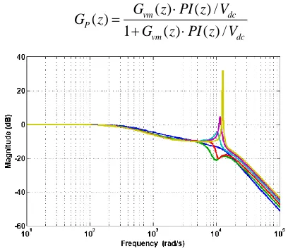
By the forward difference mapping method from the s-domain to the z-domain, the discrete transfer function of the normal PI controller can be transformed into (9), where Ts is the sampling (switching) period. Then, if Gvm(z) represents the z-plane transformed version (forward difference mapping) of the transfer function Gvm(s) in (6), its closed-loop z-domain transfer function Gp(z) with PI control is expressed by (10). To suppress the resonant peak of Gvm(z) in Fig. 5(a) over the full duty cycle range, the PI control parameters should be sufficiently small due to the RHP zeros when the duty cycle falls below ½; hence the dynamic response of the inner closed-loop is slow. For the specification in Table 3, the PI parameters are selected as P=0.4, I=600, which sets the cross-over frequency of the open loop transfer function Gvm(z)PI(z) to about 200Hz, ensuring sufficient stability margin to adapt to a wide load range variation and other disturbances. Then, the amplitude Bode plot of the inner closed-loop system Gp(z), with dc-link voltage normalization, drawn in Fig. 7, still has high resonant peaks and is not a qualified plant for repetitive control.
1 ( )
1
s
PI z P I T z
(9)
( )
( ) /
( )
1
( )
( ) /
vm dc
P
vm dc
G
z PI z V
G z
G
z PI z V
(10)
Fig. 7. Magnitude Bode plot of Gp(z) with only PI control.
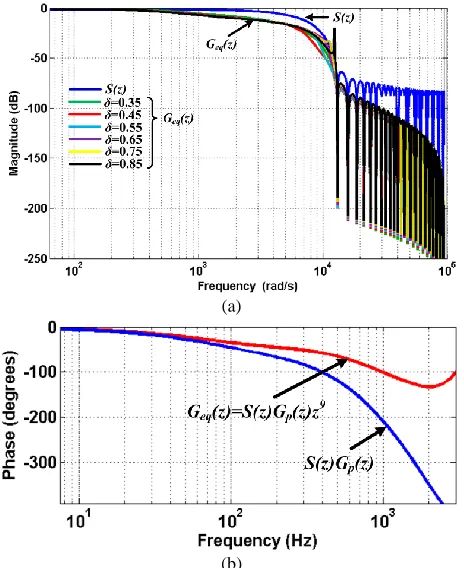
In order to eliminate the high resonant peaks of Gp(z) for large duty cycles, an additional compensator is required. Considering the low phase margin caused by the RHP zeros and the floating position of the resonance peak due to its time-variant performance, the traditional second-order low-pass filter with additional phase delay and a fixed resonance frequency ZPS notch filter are not applicable to the SQZS inverter [20]. Instead, to mitigate a set of resonant peaks for a wide duty cycle range in the SQZS inverter without deteriorating its phase margin (dynamic performance), a m order FIR ZPS compensator S(z) as in (11) with no phase lag, is employed. For the design case of Table 3, the resonance frequencies vary approximately between 1.5kHz and 2kHz as in Fig. 5(a); thus, a 17 order FIR ZPS filter S(z) with a cut-off frequency of 1.5kHz is designed in MATLAB to suppress the resonance peak to below 0dB. The S(z) parameters for this case are listed inTable 4.
0
( ) m i( i i)
i
S z a z z
(11)
Table 4. Coefficients ai for the FIR ZPS compensator S(z) in (11),m=17.
a0=0.02442; a1=0.00104; a2=0.00196; a3=0.00329; a4=0.00508; a5=0.00736; a6=0.01015; a7=0.01343; a8=0.01714; a9=0.02120; a10=0.02548;a11=0.02985; a12=0.03413; a13=0.03816; a14=0.04174; a15=0.04472;
a16=0.04697; a17=0.04836.
Further, to achieve sufficient phase margin and a fast dynamic response, a k step leading unit zk is inserted to compensate the phase-lag, particularly for the RHP zeros. Due to the data storage of repetitive control, this leading unit will not result in a non-causal system and allows a faster PI controller to improve the dynamic performance. Then, the SQZS inverter repetitive control plant can be expressed by (12), in which stability is guaranteed and the transient performance is enhanced. Specifically, k is selected to be 9 in this design case.
( ) k ( ) ( )
eq p
G z z S z G z
(12)
With all parameters now known in this case study, the [image:6.612.337.541.44.221.2] [image:6.612.48.298.170.231.2]
with k=9 and S(z)Gp(z) without phase-leading compensation are both displayed in Fig. 8(b), where the leading unit zk is able to significantly increase the phase margin to realize an improved closed-loop bandwidth. A compensated equivalent plant suitable for repetitive control can now be achieved, as in (12).
(a)
(b)
Fig. 8. Compensation effects: (a) magnitude response of Geq(z) and
S(z) and (b) phase compensation at δ=0.35.
3) Internal model design for plug-in repetitive control The repetitive controller with a fast feed-forward path is shown in the outer layer of Fig. 6. The discrete implementation of the internal model of repetitive control is expressed by (13), where Kr is the gain coefficient to adjust the tracking error convergence rate and Q(z) is a low-pass filter to guarantee stability at high frequencies [27]. By periodic integration, any repeatable disturbances can be accumulated in the output; thus high gains for these periodic signals can be achieved in (13), where N is number of sampling points within one fundamental period.
( )
1 ( )
N r
rp N
z K
G z
Q z z
(13)
Based on Fig. 6 and (13), for the modified plant Geq(z), the voltage tracking error Er(z) is expressed in (14). To ensure repetitive controller stability, the condition in (15) should be satisfied according to the small gain theorem [28]. This reveals that the magnitude of |𝐻(𝑒𝑗𝜔𝑇𝑠)| should always be less
than unity when ω changes from zero to 𝜋𝑓𝑠 (Nyquist frequency).
(1 ( ))( ( ))
( ) ( )
( ) ( )
(1 ( ))( ( ))
( ) ( ) ( ) N p ref N r eq N p d N r eq
G z z Q z
Er z V z
z Q z K G z G z z Q z
V z z Q z K G z
(14)
(
)
(
)
(
)
(
)
(
)
(
)
1
1
where
[0,
],
j Ts j Ts j Ts r eq
j Ts j kTs j Ts j Ts
r p
s
s s
H e
Q e
K G
e
Q e
e
K S e
G e
T
T
f
(15)
In practice, to ensure sufficient stability margin, Q(z) can be selected as a close-to-unity constant (such as 0.95) or a low-pass filter, which is able to ensure sufficiently high magnitude gain in Grp(z) within the baseband. Thus, provided the reference voltage Vref and disturbance Vd are both purely repetitive as in (16), by viewing Q(z) as 1 in the low frequency range and substituting it into (14), the tracking error Er(z) can be expressed by (17). This means that after each fundamental period, the magnitude of error Er(z) can be attenuated to H(z) times its previous value. Therefore, to ensure stability and increase the convergence rate, H(z) must fall within the unity circle and should be as small as possible.
( ) ( ) ( ) ( ) N d d N ref ref
z V z V z
z V z V z
(16)
( )
( )
( )
N
z
Er z
H z Er z
(17)
In the frequency domain, (14) can be rewritten as (18) with𝑇(𝑒𝑗𝜔𝑇𝑠) being expressed by (19). By decreasing the
magnitude of the term 𝑇(𝑒𝑗𝜔𝑇𝑠), the harmonic rejection ability
can be enhanced and the steady-state error of the repetitive controller is minimized. Specifically, zero steady-state error can be achieved at frequency ω, where 𝑄(𝑒𝑗𝜔𝑇𝑠) = 1.
( ) ( ) . 1 ( ) ( )
( ) . 1 ( ) ( )
j Ts j Ts j Ts j Ts
p ref
j Ts j Ts j Ts
p d
Er e T e G e V e
T e G e V e
(18)
1 ( )
( )
1 ( )
j Ts j Ts j Ts Q e T e H e
(19)
For better convergence performance, Q(z) should not introduce any additional phase delay into the control loop. Therefore, for low distortion in the SQZS converter output voltage, a FIR structure ZPS low-pass filter is designed for Q(z) with a 3kHz cut-off frequency, for the case in Table 3. The expression of Q(z) is indicated in (20) with the coefficients calculated in MATLAB, listed in Table 5.
0
( ) n i( i i)
i
Q z b z z
(20) Table 5. Coefficients bi for the FIR ZPS low-pass filter Q(z) in (20), n=6.
b0=0.59961; b1=0.21864; b2=-0.01795; b3=0.0063; b4=-0.00624; b5=0.0008; b6=0.00007.
To highlight the effect of Q(z), the stability constraint of (15) is plotted in Fig. 9, where the vector 𝐻(𝑒𝑗𝜔𝑇𝑠) should not
exceed the unity circle. Due to the design demand, in low frequency range, 𝑄(𝑒𝑗𝜔𝑇𝑠) should be close to 1 as interpreted
[image:7.612.57.289.111.395.2]8 case in Table 3, the designed gain of the FIR ZPS filter
𝑄(𝑒𝑗𝜔𝑇𝑠) in (20) and Table 5 can be maintained as 0.98 up to
2 kHz, which is satisfactory to ensure sufficient lower order harmonic rejection. With increasing frequency, the phase delay of 𝐺𝑒𝑞(𝑒𝑗𝜔𝑇𝑠)
increases, while its magnitude decreases.
This makes the 𝐾𝑟𝐺𝑒𝑞(𝑒𝑗𝜔𝑇𝑠) vector rotate closer to the imaginary axis, as shown by the dashed line in Fig. 9. Due to the high frequency attenuation effect of Q(z), the unity circle around the terminal of vector Q(z) moves left (dashed line) with an increase of frequency, which helps maintain the stability margin by ensuring sufficient distance from 𝐻(𝑒𝑗𝜔𝑇𝑠) [image:8.612.46.250.209.485.2]to the new circle (dashed line). For the spectrum range above the cut-off frequency, the magnitude of Geq(z) falls off rapidly, as in Fig. 8.
[image:8.612.362.512.340.669.2]Fig. 9. Operational stability explanation.
Fig. 10. Vector 𝐻(𝑒𝑗𝜔𝑇𝑠) locus.
The proportional gain of the repetitive controller Kr is usually a real number smaller than 1. A larger Kr produces faster error convergence but less stability margin, as it will determine the length of 𝐾𝑟𝐺𝑒𝑞(𝑒𝑗𝜔𝑇𝑠) (thus, also 𝐻(𝑒𝑗𝜔𝑇𝑠)) in Fig. 9. The trajectory of 𝐻(𝑒𝑗𝜔𝑇𝑠) in the complex plane is
drawn in Fig. 10 for Kr=1 at the operational points of minimum and maximum duty cycle δ. The stability margin is guaranteed with the selected control parameters for the SQZS inverter design case inTable 3.
Fig. 11. Open loop gain Grp(z)Geq(z) amplitude response.
With all the design parameters known, the discrete open loop transfer function of the SQZS inverter with the proposed plug-in repetitive control strategy can be expressed as
𝐺𝑟𝑝(𝑒𝑗𝜔𝑇𝑠)𝐺𝑒𝑞(𝑒𝑗𝜔𝑇𝑠), and its amplitude gains under the full duty cycle variation range are shown in Fig. 11 (Kr= 1). The repetitive controller is able to attenuate the lower order distortion in the baseband by increasing its open loop gain at integer times of the fundamental frequency. Due to the use of FIR ZPS compensator S(z) and low-pass filter Q(z), high frequency disturbance can be suppressed significantly. The effective bandwidth is extended compared to conventional methods, as shown in Fig. 11.
IV. SIMULATION AND EXPERIMENT VERIFICATION
To verify the effectiveness of the proposed control scheme, simulation and experimentation on the FSTP SQZS inverter have been performed.
A. Simulation Tests
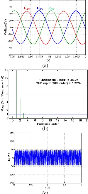
The simulation model of the topology in Fig. 2 is based on the specification in Table 3; thus, the desired output line-to-line voltage peak value is 100V (57.7V phase voltage) in the FSTP SQZS inverter. Initially, it operates with only the inner PI controller of Fig. 6, with parameters P=0.4 and I=600, which is achieved by considering the relative stability indicators.
(a)
(b)
(c)
Fig. 12. FSTP-SQZS inverter with PI controller: (a) output phase voltage waveforms, (b) fundamental magnitude and low order harmonic distribution for phase A output voltage; and (c) steady state error caused by PI control.
[image:8.612.74.273.599.721.2](mainly 2nd order); and the calculated baseband (up to 20th order) total harmonic distortion (THD) is 5.3%. This is consistent with the theoretical analysis of the PI controlled SQZS converter with low bandwidth and non-uniform gains at different operating points.
To eliminate the low order harmonic distortion and improve the reference tracking accuracy, repetitive control is employed, initially without compensator S(z) but the PI parameters remain the same. The repetitive controller has a magnifying effect on the magnitude gain, including the resonant peaks. Due to the absence of S(z), the proportional gain of the internal model Kr has to be decreased to guarantee stability. In this case, Kr is chosen to be 0.01. From Fig. 13(b), increased fundamental voltage magnitude and reduced 2nd order harmonic distortion can be achieved. However, in Fig. 13(c), the error convergence rate is slow due to small Kr.
(a)
(b)
(c)
Fig. 13. FSTP-SQZS inverter using repetitive control without compensator S(z) and Kr=0.01:(a) output phase voltage waveforms,
(b) fundamental magnitude and low order harmonic distribution for phase A output voltage; and (c) error convergence process.
By incorporating compensator S(z) into the control loop, the proportional gain Kr of the repetitive controller can be increased. With S(z) based on Table 4 and Kr=0.8, Fig. 14(b) shows that the fundamental voltage is able to precisely track the reference and low order harmonic components can be eliminated; hence, almost zero steady-state-error is obtained; and the error convergence rate significantly improves with a settling time of less than 0.2s, as illustrated in Fig. 14(c).
(a)
(b)
(c)
Fig. 14. FSTP-SQZS inverter using the proposed repetitive control scheme including S(z) and Kr=0.8: (a) output phase voltage
waveforms; (b) fundamental magnitude and low order harmonic distribution for phase A output voltage; and (c) error convergence process.
(a) (b)
(c)
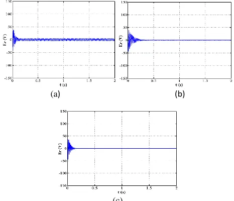
Fig. 15. Error convergence comparison for the plug-in repetitive controller with different parameters: (a) Q(z)=0.95, Kr=0.8, (b) Q(z)
[image:9.612.364.512.42.373.2] [image:9.612.98.248.233.551.2] [image:9.612.322.555.427.627.2]10 finally degrades the ability for lower order harmonic rejection.
Comparison between Fig. 15(a) and (c) reveals that Q(z) significantly influences the steady-state error.
B. Experimental Results
[image:10.612.358.516.128.573.2]A MOSFET based SQZS FSTP inverter is used for practical operational validation purposes. Due to the high voltage stress on the power switches in the SQZS converter (and other ISCs), the dc-link voltage and ac line-to-line peak voltage are scaled down to 40V and 32V (power rating is 200W) respectively, while the other parameters are maintained as in Table 3. With this arrangement, the original pole-zero positions of the SQZS converter design case are unchanged. Since the control design diagram in Fig. 6 has an 1/Vdc stage to normalize the converter model to unity (with 0dB open-loop gain in baseband), the previously selected parameters for the PI controller, S(z), phase-leading compensator, and the internal model (Q(z) and Kr), remain valid (provided the 1/Vdc stage is included).
Fig. 16. Photograph of the experimental rig.
The control strategy of the FSTP SQZS inverter is realized on a Texas Instrument TMS320F280335 DSP platform with a sampling frequency equal to switching frequency (30 kHz). The power switches are RFP4668PBF MOSFETs and the overall experiment setup is shown in Fig. 16.
(a)
[image:10.612.104.244.247.331.2](b)
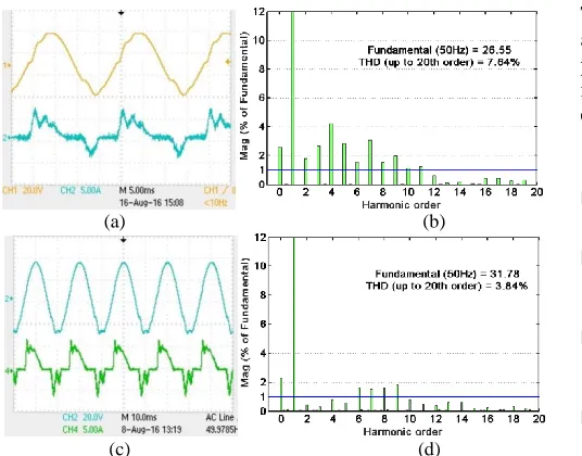
Fig. 17. Experimental results with conventional PI control: (a) three-phase output voltage and (b) fundamental magnitude and low order harmonic distribution for phase A output voltage.
Initially, conventional PI control for the FSTP SQZS inverter is tested with the results in Fig. 17, where the achieved fundamental magnitude is much lower than the desired reference. Also, due to the inadequate bandwidth, the
voltage waveform deviates from the pure sinusoid by considerable 2nd order harmonics.
Next, the three-phase output voltage and FFT analysis with the proposed repetitive control and 2.5Ω resistive load are given in Fig. 18, where all low harmonic components are less than 1% of the fundamental except a residual dc component due to the transducer zero-point 1% calibration error.
(a)
(b)
(c)
(d)
Fig. 18. Experiment results using proposed repetitive control strategy for FSTP-SQZS inverter: (a) three-phase output voltages; and fundamental magnitude and low order harmonic distribution for the output voltages of (b) phase A; (c) phase B; and (d) phase C.
[image:10.612.98.251.398.641.2]of the SQZS inverter output voltage when the load is step changed from 6Ω to 3Ω. The converter output voltage quickly tracks the reference.
(a) (b)
(c) (d)
(e)
Fig. 19. FSTP-SQZS inverter with different load conditions: (a) phase voltage and current with 2.5Ω load; (b) line-to-line voltage and converter output current with 5Ω+10mH load; (c) balanced three-phase line-to-line voltage with unbalanced load (5.6Ω for three-phase A and C, 3Ω for phase B); (d) three-phase unbalanced current; and (e) voltage transient performance during load step change (6Ω to 3Ω).
(a) (b)
[image:11.612.47.300.53.417.2](c) (d)
Fig. 20. Experiment results with a nonlinear load (diode rectifier with 300μF capacitor and 10Ω resistor): for PI control (a) voltage and current waveforms; and (b) fundamental magnitude and low order
harmonic distribution; and with repetitive control (c) voltage and current waveforms; and (d) fundamental magnitude and low order harmonic distribution.
These experimental results imply that both the steady-state and dynamic performance of the SQZS inverter can be improved by using the proposed plug-in repetitive control scheme with a ZPS compensation network.
Fig. 20(a) and (b) give the output voltage and current waveform of the SQZS inverter using PI control under a typical rectifier nonlinear load. Due to limited bandwidth and poor harmonic rejection ability, the output voltage deviates from its reference with inadequate fundamental component magnitude and significant low order harmonics. But the results in Fig. 20(c) and (d) with the proposed repetitive control strategy, maintain the desired fundamental magnitude and suppress the dominant low order harmonics.
V. CONCLUSIONS
A generic digital plug-in repetitive control strategy has been proposed for a series of high-order wide-output range impedance source converters (HOWO-ISCs). Specifically, a four-switch three-phase (FSTP) semi-quasi-Z-source (SQZS) islanded mode inverter was adopted as a representative case study. The time-variant characteristics for HOWO-ISCs with non-uniform gains in their transfer function over a fundamental period were analyzed, which leads to inherent lower order harmonic distortion in the output voltage during open-loop operation.
The proposed repetitive control strategy eliminates the reference tracking error for the HOWO-ISCs using a single loop, which outperforms conventional proportional-integral (PI) and proportional-resonant (PR) methods with multiple parallel loops for suppressing all low order harmonics. In the proposed scheme, with the designed finite impulse response (FIR) zero-phase-shift (ZPS) compensator and phase-leading unit, an extended bandwidth is obtained by overcoming the initial phase-lag caused by right-half-plane (RHP) zeros; furthermore, the internal model of the repetitive control unit offers increased loop gain with a wide frequency range. Therefore, accurate reference tracking, fast convergence rate, and robust stability can be achieved. A design procedure of the proposed controller has been presented for a FSTP-SQZS islanded inverter, which has been validated by simulation and experimental results.
REFERENCES
[1] T. Adefarati and R. C. Bansal, "Integration of renewable distributed generators into the distribution system: a review," IET Renewable Power Generation, vol. 10, pp. 873-884, 2016.
[2] L. Bangyin, D. Shanxu, and C. Tao, "Photovoltaic DC-Building-Module-Based BIPV System-Concept and Design Considerations,"
Power Electronics, IEEE Transactions on, vol. 26, pp. 1418-1429, 2011.
[3] X. Hu and K. J. Tseng, "Integration of Multiple Modularized Distributed Energy Resource Devices Into AC Grid of Buildings: Issue of Active Power Circulation," IEEE Transactions on Industrial Electronics, vol. 61, pp. 6118-6127, 2014.
[4] L. Zhang, K. Sun, L. Feng, H. Wu, and Y. Xing, "A Family of Neutral Point Clamped Full-Bridge Topologies for Transformerless Photovoltaic Grid-Tied Inverters," IEEE Transactions on Power Electronics, vol. 28, pp. 730-739, 2013.
[image:11.612.46.314.492.702.2]12 Emerging and Selected Topics in Power Electronics, vol. 3, pp.
901-917, 2015.
[6] M. Gao, M. Chen, C. Zhang, and Z. Qian, "Analysis and Implementation of an Improved Flyback Inverter for Photovoltaic AC Module Applications," IEEE Transactions on Power Electronics, vol. 29, pp. 3428-3444, 2014.
[7] D. Meneses, F. Blaabjerg, Garci, x, O. a, and J. A. Cobos, "Review and Comparison of Step-Up Transformerless Topologies for Photovoltaic AC-Module Application," Power Electronics, IEEE Transactions on, vol. 28, pp. 2649-2663, 2013.
[8] Y. P. Siwakoti, F. Z. Peng, F. Blaabjerg, P. C. Loh, and G. E. Town, "Impedance-Source Networks for Electric Power Conversion Part I: A Topological Review," IEEE Transactions on Power Electronics, vol. 30, pp. 699-716, 2015.
[9] Y. P. Siwakoti, F. Z. Peng, F. Blaabjerg, P. C. Loh, G. E. Town, and S. Yang, "Impedance-Source Networks for Electric Power Conversion Part II: Review of Control and Modulation Techniques," IEEE Transactions on Power Electronics, vol. 30, pp. 1887-1906, 2015. [10] C. Dong, J. Shuai, Y. Xianhao, and P. Fang Zheng, "Low-Cost
Semi-Z-source Inverter for Single-Phase Photovoltaic Systems," Power Electronics, IEEE Transactions on, vol. 26, pp. 3514-3523, 2011. [11] L. Peng, G. P. Adam, H. Yihua, D. Holliday, and B. W. Williams,
"Three-Phase AC-Side Voltage-Doubling High Power Density Voltage Source Converter With Intrinsic Buck–Boost Cell and Common-Mode Voltage Suppression," Power Electronics, IEEE Transactions on, vol. 30, pp. 5284-5298, 2015.
[12] A. Darwish, A. Massoud, D. Holliday, S. Ahmed, and B. Williams, "Single-stage Three-phase Differential-mode Buck-Boost Inverters with Continuous Input Current for PV Applications," Power Electronics, IEEE Transactions on, vol. PP, pp. 1-1, 2016.
[13] M. S. Diab, A. Elserougi, A. M. Massoud, A. S. Abdel-Khalik, and S. Ahmed, "A Four-Switch Three-Phase SEPIC-Based Inverter," Power Electronics, IEEE Transactions on, vol. 30, pp. 4891-4905, 2015. [14] J. Knight, S. Shirsavar, and W. Holderbaum, "An improved reliability
Cuk based solar inverter with sliding mode control," IEEE Transactions on Power Electronics, vol. 21, pp. 1107-1115, 2006. [15] F. Z. Peng, "Z-source inverter," in Industry Applications Conference,
2002. 37th IAS Annual Meeting. Conference Record of the, 2002, pp. 775-781 vol.2.
[16] A. Darwish, Y. Wang, D. Holliday, and S. Finney, "Operation and control design of new Three-Phase inverters with reduced number of switches," in 2016 International Symposium on Power Electronics, Electrical Drives, Automation and Motion (SPEEDAM), 2016, pp. 178-183.
[17] R. Tymerski and V. Vorperian, "Generation, Classification and Analysis of Switched-Mode DC-to-DC Converters by the Use of Converter Cells," in Telecommunications Energy Conference, 1986. INTELEC '86. International, 1986, pp. 181-195.
[18] T. Ying-Yu, O. Rong-Shyang, J. Shih-Liang, and C. Meng-Yueh, "High-performance programmable AC power source with low harmonic distortion using DSP-based repetitive control technique,"
IEEE Transactions on Power Electronics, vol. 12, pp. 715-725, 1997. [19] Z. Keliang and W. Danwei, "Digital repetitive learning controller for
three-phase CVCF PWM inverter," Industrial Electronics, IEEE Transactions on, vol. 48, pp. 820-830, 2001.
[20] Z. Kai, K. Yong, X. Jian, and C. Jian, "Direct repetitive control of SPWM inverter for UPS purpose," Power Electronics, IEEE Transactions on, vol. 18, pp. 784-792, 2003.
[21] C. Younghoon and L. Jih-Sheng, "Digital Plug-In Repetitive Controller for Single-Phase Bridgeless PFC Converters," Power Electronics, IEEE Transactions on, vol. 28, pp. 165-175, 2013. [22] M. Zhang, L. Huang, and W. Yao and Z. Lu, "Circulating Harmonic
Current Elimination of a CPS-PWM-Based Modular Multilevel Converter With a Plug-In Repetitive Controller," IEEE Transactions on Power Electronics, vol. 29, pp. 2083-2097, 2014.
[23] H. Liqun, Z. Kai, X. Jian, and F. Shengfang, "A Repetitive Control Scheme for Harmonic Suppression of Circulating Current in Modular Multilevel Converters," Power Electronics, IEEE Transactions on, vol. 30, pp. 471-481, 2015.
[24] A. Ghasemi, E. Adib, and M. R. Mohammadi, "A new isolated SEPIC converter with coupled inductors for photovoltaic applications," in
2011 19th Iranian Conference on Electrical Engineering, 2011, pp. 1-5.
[25] M. B. d. R. Correa, C. B. Jacobina, E. R. C. d. Silva, and A. M. N. Lima, "A General PWM Strategy for Four-Switch Three-Phase
Inverters," IEEE Transactions on Power Electronics, vol. 21, pp. 1618-1627, 2006.
[26] H. L. Broberg and R. G. Molyet, "A new approach to phase cancellation in repetitive control," in Industry Applications Society Annual Meeting, 1994., Conference Record of the 1994 IEEE, 1994, pp. 1766-1770 vol.3.
[27] A. Garcia-Cerrada, O. Pinzon-Ardila, V. Feliu-Batlle, P. Roncero-Sanchez, and P. Garcia-Gonzalez, "Application of a Repetitive Controller for a Three-Phase Active Power Filter," IEEE Transactions on Power Electronics, vol. 22, pp. 237-246, 2007.
[28] Z. Keliang and D. Wang, "Digital repetitive controlled three-phase PWM rectifier," IEEE Transactions on Power Electronics, vol. 18, pp. 309-316, 2003.
Yachao Wang (S’15) received the B.Sc. degree in Department of Electrical Engineering, Xi’an Jiaotong University, Xi’an, China, in 2009, and M.Sc. degree in Applied Power Electronics, Zhejiang University, Hangzhou, China, in 2012, respectively.
She is currently working towards her Ph.D. degree at Electronic & Electrical Engineering Department, University of Strathclyde, Glasgow, UK.Her research interests include high effeciency power electronics converters and the utility applications.
Ahmed Darwish received the B.Sc. and M.Sc. degrees in electrical engineering from the Faculty of Engineering, Alexandria University, Alexandria, Egypt, in 2008 and 2012, respectively, and the Ph.D. degree in electric engineering from the Department of Electronic and Electrical Engineering, University of Strathclyde, Glasgow, U.K., in 2015.
From 2009 to 2012, he was a Research Assistant at Texas A&M University at Qatar, Doha, Qatar. He is currently a Research Associate with PEDEC Group at the University of Strathclyde. His research interests include dc–dc converters, multilevel converters, electric machines, digital control of power electronic systems, energy conversion, renewable energy, and power quality.
Derrick Holliday has research interests in the areas of power electronics, electrical machines and drives. In 1995 he obtained the degree of PhD from Heriot Watt University and, since then, has held full-time academic posts at the Universities of Bristol and Strathclyde. He has authored or co-authored over 70 academic journal and conference publications. He is currently leading industrially funded research in the field of power electronics for HVDC applications, and is co-investigator on research programs in the fields of photovoltaic systems and the interface of renewable energy to HVDC systems.
