Theses
2019
Point Spread Function Determination in the
Scanning Electron Microscope and its Application
in Restoring Images Acquired at Low Voltage
Mandy C. Nevins
Follow this and additional works at:https://scholarworks.rit.edu/theses
This Dissertation is brought to you for free and open access by RIT Scholar Works. It has been accepted for inclusion in Theses by an authorized administrator of RIT Scholar Works. For more information, please [email protected].
Recommended Citation
Point Spread Function Determination in the
Scanning Electron Microscope and its Application in
Restoring Images Acquired at Low Voltage
by
Mandy C. Nevins
B.S. University of Wisconsin-Eau Claire, 2014
A dissertation submitted in partial fulfillment of the
requirements for the degree of Doctor of Philosophy
in the Chester F. Carlson Center for Imaging Science
College of Science
Rochester Institute of Technology
2019
Signature of the Author
_______________________________________________________Accepted by
_________________________________________________________________ii
CHESTER F. CARLSON CENTER FOR IMAGING SCIENCE COLLEGE OF SCIENCE
ROCHESTER INSTITUTE OF TECHNOLOGY ROCHESTER, NEW YORK
CERTIFICATE OF APPROVAL
Ph.D. DEGREE DISSERTATION
The Ph.D. Degree Dissertation of Mandy C. Nevins has been examined and approved by the dissertation committee as satisfactory for the
dissertation required for the Ph.D. degree in Imaging Science
________________________________________________ Prof. Richard Hailstone, Dissertation Advisor
________________________________________________ Dr. Lea Michel, External Chair
________________________________________________ Dr. Eric Lifshin
________________________________________________ Dr. Nathan Cahill
iii
To my darling husband
iv
Point Spread Function Determination in the
Scanning Electron Microscope and its Application in
Restoring Images Acquired at Low Voltage
by
Mandy C. Nevins Submitted to the
Chester F. Carlson Center for Imaging Science in partial fulfillment of the requirements
for the Doctor of Philosophy Degree at the Rochester Institute of Technology
Abstract
v
Acknowledgements
This has really been quite the journey! I am so thankful to have been graced with the support, wisdom, and love of so many people along this challenging and meaningful path.
Firstly, I’d like to thank Prof. Richard Hailstone for introducing me to the tiny worlds within electron microscopy and advising me in my doctoral research. His quiet enthusiasm for science on the nanoscale inspired me, and his guidance has helped me develop into a scientist capable of performing independent research, which was the whole idea! I am thankful for the example he set as an approachable lab manager who is always open to assist students and microscope-users in solving their problems. Thank you for helping me stay determined, even when the microscopes and software decided to be less than user-friendly.
I would like to extend my gratitude to Prof. Eric Lifshin for his mentorship and
collaboration in my thesis work. Thank you for bringing all your know-how and questions about the SEM point spread function to the Rochester Institute of Technology (RIT). Additional thanks to Matthew Zotta for his work in developing the Aura Workstation on which much of my
research was performed, Kathy Quoi for her insight regarding SEM simulations, and Jeffrey Moskin for providing the funding necessary to launch the Aura Workstation.
While in the world of nano, I would also like to thank my friend and lab mate, Najat Alharbi. Our lab may have been small, but it is just like the microscopic subjects we studied…. small but scientifically mighty.
I am appreciative of my entire thesis committee, including Dr. Nathan Cahill, and Dr. Lea Michel. Thank you for supervising and enriching my work! I am grateful to Dr. Cahill for
sharing his mathematical expertise and bringing attention to important aspects of this work which may not have been addressed otherwise. Thank you to Dr. Michel for contributing to this discussion and for being an excellent role model of a woman in science.
vi
friends at RIT, including Grant Anderson, Emily Berkson, Lucy Chu, Ryan Ford, Sanghui Han, Kushal Kafle, Michal Kucer, Elisabeth McClure, Elizabeth Moore, Emily Myers, Lauren Taylor, Anton Travinsky, Jared Van Cor, Oesa Weaver, and Jacob Wirth. Thank you for sharing your encouragement, problem-solving, and love of science.
Rochester would not have felt like home with the friendship and care of Bridget Connolly, Matthew Rasmussen, Vera Delfavero, Anne Namocatcat, John McDermott, and the late Betsy McDermott. Thank you all. So much.
Before Rochester, I had the opportunity to study with the amazing physics folks at the University of Wisconsin-Eau Claire (UWEC). A big thank you to Dr. Erik Hendrickson for helping me through my foundational physics courses with countless office hours and for encouraging me to apply for a Research Experience for Undergraduates (my first experience with true scientific research, which inspired me to pursue my PhD)! Another great deal of gratitude is owed to Dr. Lauren Likkel for fueling my excitement for science and for improving my confidence as a speaker of science through many fun, cheesy planetarium presentations. Additional thanks to Dr. Nathan Miller, Dr. Kim Pierson, Dr. Matt Evans, Dr. Scott Whitfield, and Dr. George Stecher for sharing their knowledge and creating a welcoming environment for every student. A special note of thanks to Dr. Tom Lockhart for his delightful insight that a PhD is truly a test of stubbornness, as you have to try and try again when all your experiments break and break again.
Sincere thanks to all those friends who helped me learn about the brilliant, challenging subject that is physics, including the late Roxanne Accola, Shalaine Buehl, Ryan McCarty, Jake Pederson, Blake Smith, Sean O’Connell, James Truchinski, and Michael Yohn. Thank you also to my friends in the languages, businesses, and other sciences, for sharing your diverse
knowledge and support, including Becca Anderson, Josh Bauer, Colleen Carhuff, Jon Ecker, John Fisher, Katie Fisher, Robert Fisher, Oscar Lopez-Martinez, Steve Searing, and Mitch Wood.
vii
teaching me how outline, organize, and write about research, setting me on the path to tackle a thesis! Sincere thanks to Doug Benton for sharing his scientific know-how, his encouragement, and for preparing me to succeed. Thank you to all of those who shared their friendship
throughout that time, especially Ben Burnett for his exuberant confidence and sense of self which inspired me to embrace my inner scientist.
I give immense gratitude to my oldest friend, Tanika Reckner. She has seen me and supported me through it all, always there to lend a hand or an ear (and always willing to give more of herself than what is asked of her). Thank you for always being you, no matter what.
I have so much appreciation and admiration for my parents, Ron and Lori Neumann. They helped me grow into the person I was meant to be, and have been infinitely supportive on this journey. Thank you for showing me the value of hard work, and also the significance of bringing kindness and compassion into whatever I do. I am so, so lucky to have such a wonderful family supporting me. Thank you to my brothers and their wives, Michael and Christina Mroz, and Christian and Courtney Neumann, for living and working with love and for modeling joyous strength in family and faith. Thank you to my nieces and nephew, Hannah, Kaleb, Elsa, and Ellianna Mroz for reminding me about all the exciting wonders and possibilities in this world. Thank you to all of my family, and please know that your support has meant so much to me. I would also like to give a shout-out to the crazy smart and generally crazy Nevins bunch who welcomed me into their family and have always been willing to share their stories and “gifts”. A special note of thanks to Dr. Amanda Nevins for providing much-appreciated wisdom about navigating graduate school and PhD research.
viii
Author Publications
* indicates the authors contributed equally on this publication.
† indicates that a modified version of this publication is included in this dissertation.
Refereed Publications
† Zotta MD*, Nevins MC*, Hailstone RK and Lifshin E (2018) The determination and application of the point spread function in the scanning electron microscope. Microscopy and Microanalysis24(4), 396-405.
Submitted/In-Review
† Nevins MC, Quoi K, Hailstone RK and Lifshin E (In Review) Exploring the parameter space
of point spread function determination for the scanning electron microscope – Part I: Effect on the point spread function. In review at Microscopy and Microanalysis.
† Nevins MC, Hailstone RK and Lifshin E (In Review) Exploring the parameter space of point
spread function determination for the scanning electron microscope – Part II: Effect on image restoration quality. In review at Microscopy and Microanalysis.
Conference Papers
Nevins MC, Zotta MD, Hailstone RK and Lifshin E (2018) Visualizing astigmatism in the
SEM Electron Probe. Microscopy and Microanalysis24(S1), 604-605.
Nevins MC, Hailstone RK, Zotta MD and Lifshin E (2017) Viability of point spread function
deconvolution for SEM. Microscopy and Microanalysis23(S1), 126-127.
Magazine Articles
ix
Contents
1
Introduction ... 1
1.1 Context ... 1
1.2 Objectives ... 1
1.3 Approach ... 2
1.4 Contributions ... 2
1.5 Thesis Layout ... 3
2
Background ... 4
2.1 Image Formation in the SEM ... 4
2.1.1 The Electron Probe ... 5
2.1.2 Electron-Matter Interaction ... 8
2.2 Low Voltage Imaging... 10
2.3 The Point Spread Function ... 13
2.4 PSF Determination and Image Restoration in the SEM ... 16
3
The Determination and Application of the Point Spread Function in the
Scanning Electron Microscope ...17
3.1 Introduction ... 17
3.1.1 Prior Efforts at PSF Determination ... 19
3.2 Materials and Methods ... 20
x
3.2.2 Image Collection and Processing ... 21
3.2.3 Reference Image Generation... 23
3.2.4 The PSF Calculation and Visualization ... 23
3.3 Results and Discussion ... 26
3.3.1 Calibration Robustness and the Effect of Beam Energy ... 26
3.3.2 Comparison of the New Method with the Knife Edge Test... 30
3.3.3 Effect of Working Distance ... 31
3.3.4 Characterization of Astigmatism ... 32
3.3.5 Electron Source Type ... 35
3.3.6 Image Restoration ... 36
3.4 Conclusions ... 38
4
Parameter Space Exploration: Effect on the Point Spread Function ...40
4.1 Introduction ... 41
4.1.1 Selection of Parameters for Study... 43
4.2 Materials and Methods ... 46
4.2.1 Calibration Samples for SEM PSF Determination ... 46
4.2.2 TEM Magnification Calibration and Particle Sizing ... 47
4.2.3 SEM ... 47
4.2.4 Particle Sizing and Profiling in SEM ... 49
4.2.5 PSF Determination ... 50
4.2.6 Parameter Space Exploration ... 50
4.3 Results and Discussion ... 53
4.3.1 PSF Calculation Parameters ... 53
4.3.2 Data Collection Parameters... 59
xi
5
Parameter Space Exploration: Effect on Image Restoration Quality ...71
5.1 Introduction ... 72
5.1.1 Selection of Parameters for Study... 74
5.2 Materials and Methods ... 75
5.2.1 SEM and Samples ... 75
5.2.2 Image Restoration through PSF Deconvolution ... 76
5.2.3 Image Quality Evaluation ... 77
5.2.4 Parameter Space Exploration ... 79
5.3 Results and Discussion ... 80
5.3.1 Restoration-specific Parameters... 80
5.3.2 PSF Calculation Parameters ... 82
5.4 Conclusions ... 91
6
Conclusion and Future Research...94
Bibliography ...98
Appendix A: Preliminary Work ...105
A.1 SEM Image Restoration using PSF Deconvolution ... 105
A.2 Fitted Gaussians as a PSF Comparison Metric ... 108
A.3 Influence of the Number of Nanoparticles on PSF Repeatability ... 110
A.4 Visual Comparison of Low Voltage Image Restoration to High Resolution Imaging 113
Appendix B: Chapter 3 Supplemental ...117
B.1. Determination of the Relationship between d25%-75% and dFWHM ... 117
B.2 Effect of Working Distance... 122
B.3 Characterization of Astigmatism ... 125
xii
Appendix C: Chapter 4 Supplemental ...130
C1. ImageJ Measurements of Particle Size... 130
C.2 ISO Measurements of Particle Size ... 132
C.3 PSF FWHMs for a Range of K and Background Correction ... 135
C.4 Profiles of Simulated Particles for Comparison of BSEvsSE and GridVsKapton ... 139
C.5 Single Particle Images and Average Profiles for Comparison of Experimental and Simulated Data on the TEM Grid ... 141
Appendix D: Chapter 5 Supplemental ...142
D.1 Images and Curves for a Range of λ ... 142
D.2 Images and Curves for Reference Particle Size Comparison (λ = 17, 57, 77) ... 144
D.3 Images and Curves for K Comparison (λ = 17, 57, 77) ... 148
D.4 Images and Curves for PSF Background Correction Comparison (λ = 17, 57, 77) ... 152
Appendix E: Image Restoration Examples ...156
E.1 Carbon Nanotubes ... 156
E.2 Mouse Brain ... 161
E.3 Carbon Fiber ... 166
1
1
Introduction
1.1
Context
A point spread function (PSF) is the impulse response of an imaging system. An image can be described as the convolution of the PSF and the scene being imaged. Knowledge of the PSF can be utilized for system characterization and to restore image quality. Addressing the resolution limits in the scanning electron microscope (SEM) requires the ability to characterize the microscope’s focused electron beam (i.e., PSF). PSF deconvolution could provide a versatile, low-cost solution for improving SEM image quality, particularly at low voltages. Measuring the PSF of an SEM is difficult because an image is gathered pixel-by-pixel, instead of all at once, by rastering a focused beam of electrons across a sample-of-interest, and collecting the signal generated by electron-matter interactions at each pixel.
1.2
Objectives
1.3
Approach
Images of calibration samples (e.g., nanoparticle dispersions) and samples-of-interest are captured on a TESCAN MIRA3 field emission scanning electron microscope (FESEM). The PSF can be determined by comparing the average observed particle with a simulated reference particle. The PSF can be studied on its own or used to perform PSF deconvolution on any image taken with the same beam shape as the calibration image. The PSF determination method is evaluated under a range of SEM operating conditions to establish the method’s robustness and practicality. Applications of this PSF determination method are presented. The parameter space of the PSF determination method is explored in terms of the effects on the resulting PSF and image restorations (PSF deconvolution). The Aura Workstation was utilized for PSF determination and deconvolution.
1.4
Contributions
The PSF determination method presented here is the first to provide a full visualization and measurement of the SEM electron probe. This enables new research into SEM probe shape and behavior which was previously inaccessible, with applications in microscope characterization, maintenance, and image restoration.
1.5
Thesis Layout
Chapter 1 – Introduction provides an overview of the research presented in this thesis.
4
2
Background
2.1
Image Formation in the SEM
Electron-optical systems generate images using electron wavelengths which are orders-of-magnitude smaller than wavelengths of visible light. This means the electron microscope has the capability to examine materials at a level of detail much finer than is capable with a traditional light microscope. Resolution on the order of nanometers is achievable by high-end modern SEM technologies, allowing scientists to examine specimens with nanoscale detail. But, achieving this resolution is dependent on many factors, importantly the electron probe size and current, energy of beam electrons, and material composition.
In an SEM (Figure 2-1), the image is generated pixel-by-pixel by focusing an electron beam onto a bulk sample and then rastering the beam over an area (Figure 2-2). To perform imaging with electrons, the SEM gun, column, and chamber must be under high vacuum. This ensures that the electrons are not deflected by air molecules during focusing, imaging, and signal collection. A voltage, usually on the order of kilovolts, is applied to a metal filament or crystal (the electron gun) which emits electrons. The emitted electrons travel through magnetic lenses which focus the electrons into a small electron probe.
until all pixels have been collected, meaning the entire area to be imaged has been scanned and we have one complete image frame on our monitor.
2.1.1
The Electron Probe
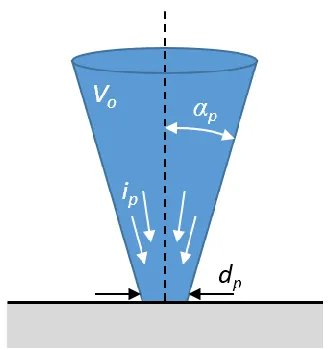
The electron beam can be defined by four main parameters where it impinges the sample-of-interest (see Figure 2-3 for visualization). The accelerating voltage, Vo, is the voltage applied to
the electron gun. (The energy of the electrons, Eo, in the beam is then equal to eVo.) The electron
probe diameter, dp, is simply the diameter of the electron beam where it makes contact with the
sample. The electron probe current, ip, is the number of electrons impinging the sample per second.
The electron probe convergence angle, α, is the half-angle of the cone of electrons which make up
[image:18.612.87.531.86.318.2]the probe at the sample. These factors play an important role in the quality and resolution of the eventual image.
The magnification of an SEM is determined by the ratio of the distance scanned on the display to the distance scanned on the sample (e.g., scanning a smaller area results in a larger magnification, because the display size is constant). But, magnification is not infinite! It is limited by the minimum electron probe size. As magnification is increased, the step size between pixels is
Figure 2-2. Raster Scan in SEM for Pixel-by-Pixel Image Collection. The electron (e-) beam is scanned across a
[image:19.612.182.434.207.649.2]decreased, and the probe size remains constant (Figure 2-4). Eventually, the step size between pixels becomes smaller than the diameter of the electron probe. This leads to “empty magnification”, where the oversampling of sample pixels results in a blurry image. Because of this, electron probe diameter is one of the limiting factors of resolution in the SEM.
An approximation of probe diameter can be found in Equation 2.1 (Bell and Erdman, 2013).
𝑑𝑒𝑓𝑓2 = 𝑑𝑑2 + 𝑑𝑠2+ 𝑑
𝑐2+ 𝑑𝑔2 (2.1)
where deff is the effective probe diameter, dd is the beam width of the Airy disc corresponding to
the diffraction limit, ds is the size of disk of least confusion caused by spherical aberration, dc is
the size of the disk of least confusion due to chromatic aberration, and dg is the minimum Gaussian
focus of the beam. These values are given by Equations 2.2-2.5.
𝑑𝑑 =
0.61𝜆
𝛼 (2.2) 𝑑𝑐 = 𝐶𝑐𝛼 (
Δ𝐸 𝐸𝑜
) (2.3)
𝑑𝑠 =1 2𝐶𝑠𝛼
3 (2.4)
𝑑𝑔 = √ 4𝑖𝑝
𝛽𝜋2𝛼2 (2.5)
Figure 2-3. Visualization of Electron Probe with Major Beam Parameters. The beam is defined by four parameters at the point where the beam impinges the sample. These parameters are the electron probe diameter, dp, electron probe
current, ip, electron probe convergence angle, αp, and the beam accelerating voltage, Vo. This illustration was inspired
[image:20.612.223.388.81.256.2]In the given equations, λ is the wavelength of the electrons, Cs and Cc are coefficients of
aberration, ΔE is the energy spread of electrons, and β is the brightness of the beam. The electron wavelength is dependent on the energy of the incoming electrons. Higher energies mean smaller wavelengths, and therefore a smaller beam width due to diffraction. The electron energy is also important when determining the contribution of lens aberrations to the beam size. As beam energy decreases, the ratio of the spread of electron energies to the beam energy (Δ𝐸/𝐸𝑜) increases. This makes chromatic aberration the dominating term for effective probe diameter at low voltage. The minimum probe size becomes larger than at high voltages, resulting in degraded resolution.
2.1.2
Electron-Matter Interaction
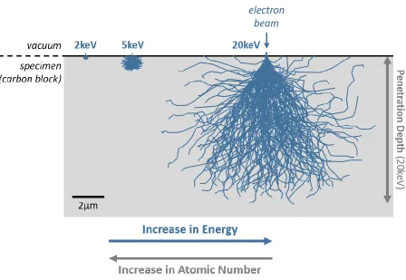
The electron beam interacts with the sample, causing the sample to emit various signals, including backscattered electrons (BSE), secondary electrons (SE), X-rays, and other types of radiation. The incoming beam electrons penetrate a certain depth into the sample, dependent on the energy of the electrons and the elemental composition of the sample (Figure 2-5). The region from which generated signal is collected is called the interaction volume. If the interaction volume is larger than the sample pixel size, signal could leak into adjacent pixels, reducing resolution (Figure 2-6).
Each signal reveals different information about the sample due to the mechanism by which the signal is generated. BSE are the original beam electrons which have scattered and then reemerged from the sample. In materials with high atomic number (Z), more high-angle scattering occurs which generates increased BSE signal. Imaging with BSE provides great contrast between
materials of different elemental composition. While the beam electron is in the sample, it may ionize atoms, creating SEs. SEs generated within a few nanometers of the surface (within the escape depth) emerge from the sample and can be collected for imaging by the SE detector. This makes SE useful for imaging surface topography. Looking at Figure 2-6, SE1 are the SE that are good for imaging, as they emerge from near where the beam impinges the sample and therefore represent the pixel currently being imaged. While exiting or once exited from the sample, BSE can instigate extraneous SE far from the beam impingement site on the sample (SE2) or from interactions with the microscope chamber (SE3). This decreases SE resolution because SE2 and SE3 add information to the overall SE signal that is not from the pixel currently being imaged.
An example of the role signal type and voltage play in image generation is given in Figure 2-7. It is important to select the appropriate microscope conditions to obtain the desired information about the material being studied.
2.2
Low Voltage Imaging
Modern SEMs typically operate at beam voltages between 2-30kV, and some have the ability to image at voltages down to tens of eV. Compared to higher voltages, lower beam voltages (<5kV) have a larger spot size (“beam footprint”) due to factors including longer electron wavelength and increased chromatic aberration. This results in reduced resolution at low voltages. But, low voltage imaging has many benefits and a variety of applications (Bell and Erdman, 2013). At low voltages, beam-sensitive samples are at reduced risk of beam damage, which can change the physical make-up of the sample. This results in images which are poor quality and difficult to interpret. Some examples of beam-sensitive samples include semiconductors (Müllerová and Frank, 2003) which are integral to modern life in objects like smartphones and other computer-based technologies, photovoltaics which harvest solar energy (Masters et al., 2015), and medical
[image:23.612.156.457.81.319.2]and biological samples (Schatten and Pawley, 2008). Lower energy electrons also cause less charging in non-conductive samples, which can eliminate the need to coat samples with a conductive film prior to imaging. Because low energy electrons do not penetrate as deeply into a sample as with high energies, the interaction volume is shallower and enables studies of sample surface topography and thin films. Lower beam energies also open up contrast mechanisms not available at high voltage (Bell and Erdman, 2013), which can be useful depending on the information a user wishes to obtain about their sample.
Unfortunately, the advantages of high voltage imaging are lost when imaging at lower voltages. Low voltages images tend to be noisy and blurry due to increased probe size and electron wavelength (i.e., diffraction limit) and a decline in signal-to-noise due to lower probe currents, a consequence of lower brightness which decreases with Eo. While higher probe currents could be
used to increase signal-to-noise, it would also increase the size of the electron probe, producing further decline in resolution. The effects of chromatic aberration is greater at low voltages which hinders resolution even more. In addition, surface contamination becomes more visible in low voltage images because the small interaction volume now contains a larger number of the contamination layers. As one can imagine, finding the optimal focus under these conditions is difficult and time-consuming, with no promise of obtaining the desired image quality.
Many advancements have been made in low voltage imaging in an attempt to counter the challenging conditions. During specimen preparation, plasma cleaning can reduce and remove carbon build-up on samples, assisting in the mitigation of contamination effects during imaging.
Higher resolutions are achievable with the development of field emission electron guns, which deliver higher brightness and smaller electron energy spread compared to earlier gun models (Egerton, 2010). Low Voltage SEMs (LVSEM) and Scanning Low Energy Electron Microscopes (SLEEM) were created specifically for the task of imaging at low voltages (Müllerová, 2001). LVSEMs are designed to emit very low energy electrons (<1keV), but can encounter limitations from lens aberrations. Aberration-corrected SEMs would lead to a major improvement in SEM performance, but systems that could account for multiple aberrations would drive the system’s complexity and cost quite high (Joy in Schatten and Pawley, 2008). Progress in aberration correction has primarily occurred in TEM and STEM, and only first steps have been made for the SEM (Hawkes, 2015).
A review of the developments in SLEEM technology is given by Frank et al., 2011. The technique introduced by SLEEM is also known as beam deceleration mode (BDM) or gentle beam mode. SLEEM instruments use a special retarding-field element to control electron energy around the specimen. A cathode lens encompasses the specimen, and excited electrons from sample emission are extracted and accelerated to an anode for collection at enhanced resolutions. Disadvantages of SLEEM include the strong electrostatic field applied at the specimen and the requirement that the specimen must be relatively smooth. Detectors are also an important variable in low voltage imaging. State-of-the-art SE and BSE detectors employ energy filtering techniques to improve the collection of low energy signals, where electron yields are low and noise becomes a greater concern (Bell and Erdman, 2013; Lewis et al., 2015).
2.3
The Point Spread Function
Addressing the issue of resolution in the SEM requires the ability to characterize the microscope, most importantly the electron probe. Understanding the shape and size of the probe opens the door to understanding how different operating conditions and technologies effect the probe, facilitating strategies for improvement. Along with microscope characterization, measuring the electron probe provides information about the system that is vital for image restoration, and also has prospective applications in microscope maintenance. In the case of the SEM, the electron probe can be described by the point spread function (PSF) of the microscope.
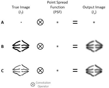
The PSF of any imaging system relates how a single point of light is transformed by the system during imaging. An imaging system with an ideal PSF (i.e., delta function) would produce an image of a perfect point, matching the input exactly. In reality, the PSF is not ideal due to factors like imperfect focusing elements and system noise, which causes the output image to be somewhat distorted compared to the scene being imaged. By measuring the PSF, the imaging system and its imperfections can be characterized, which creates potential for resolution improvement efforts.
Mathematically, an image can be represented as the convolution of the PSF and the scene being imaged, as seen in Equation 2.6.
𝐼𝑜= 𝑃𝑆𝐹 ⊗ 𝐼𝑇+ 𝜂 (2.6)
The observed image, Io, can be represented as the convolution (⊗) of the scene being imaged (true
image), IT,and the point spread function, PSF, with addition of noise, η, from the image generation
process. A visualization of the blurring process can be seen in Figure 2-8.
Normally, IT is inaccessible, as it has been changed by the PSF and has been affected by
system noise, resulting with IO. If the PSF and IO are known, careful arrangement of Equation 2.6
along with methods for handling noise allow us to use deconvolution to calculate IT. In essence,
PSF deconvolution restores image information (i.e., resolution) which has been lost due to blur or distortion by the PSF.
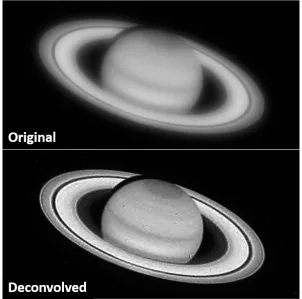
of the successful application of PSF deconvolution is in the early Hubble Space Telescope (Lindler, 1990; Lallo, 2012), where the technique was used to correct for spherical aberration caused by a flawed mirror that was not detected before launch (Figure 2-9). In microscopy, PSF deconvolution is regularly utilized in confocal microscopy (Pawley, 2006), a form of light microscopy which images samples by exciting fluorescent labels with lasers. Scientists in soft X-ray microscopy have applied PSF deconvolution for the purposes of image deblurring and improved experimental setup (Otón et al., 2016; Ekman et al., 2017). The application of PSF deconvolution in electron microscopy, specifically SEM, is the topic of recent work (Lifshin et al., 2014; Zotta, 2016) and is addressed in this thesis.
Thus far, image processing solutions for SEM have focused on image enhancement. Through enhancement, an image undergoes a mathematical transformation in an attempt to improve image quality, but the improvement is not based on information from the imaged scene
[image:27.612.126.496.92.391.2]or the system which captured the image. In electron microscopy, this includes techniques like denoising (Sim et al., 2007; Mazhari and Hasanzadeh, 2016) and edge enhancement (Bai and Zhang, 2014). This even includes “blind” deconvolution techniques (Yano and Nomura, 1993; Nakamae et al., 1994; Vanderlinde and Caron, 2007; Koshev et al., 2011; Lupini and de Jonge, 2011; Ramachandra and de Jonge, 2012; Bajic et al., 2016), which rely on estimations of the PSF because the PSF is not known. A thorough review and analysis of state-of-the-art image processing techniques utilized in electron microscopy is given by Roels et al. (2018).
PSF deconvolution presents a cost-efficient and widely applicable image restoration technique for resolution and image quality improvement in the SEM. This could introduce improvement for low voltage imaging, as well as possibly improve thermionic electron source imaging to the level of FESEM-type imaging. While the results of blind deconvolution have shown some improvement in image quality, they lack the unique knowledge of their system which is characterized by the PSF. Therefore, only an approximation of the true image can be attained by
[image:28.612.155.457.87.386.2]the blind technique. The advantage of PSF deconvolution is the ability to restore scene information to an image based on knowledge of the imaging system. Roels et al. (2018) showed that denoising methods produced higher image quality when combined with PSF deconvolution than when using denoising on its own.
2.4
PSF
Determination
and
Image
Restoration
in
the
SEM
Knowledge of the SEM PSF would be beneficial for microscope characterization, image restoration (especially at low voltages), and has potential for use in microscope maintenance. Unfortunately, the PSF is notoriously difficult to measure in the SEM. This is due to the lack of obvious point source, possible interference during the electron-matter interaction, and pixel-by-pixel image collection in the case of scanning systems. A review of methods for electron probe measurement and visualization is presented in Chapter 3.
17
3
The Determination and Application of the
Point Spread Function in the Scanning Electron
Microscope
This chapter presents a novel PSF measurement method for SEM, laying the groundwork for subsequent chapters. Knowledge of the electron probe shape (PSF) is valuable for SEM performance characterization and monitoring, as well as for modeling and simulation in computational scanning electron microscopy. For example, the PSF can characterize astigmatism and also open up the opportunity to study the relationship between beam energy, beam current, working distance, and beam shape and size in ways which were previously inaccessible. In addition, the PSF can be used for the purpose of deconvolution to improve the resolution and quality of images obtained using various electron sources (e.g., thermionic, FEG, or Schottky). The presented method represents an improvement over previous methods for measuring the SEM beam and several practical applications are described. Preliminary work to that presented in this chapter can be found in Appendix A.
3.1
Introduction
larger than the spacing, causing what is known as oversampling (Goldstein et al., 2018). When this happens, the information obtained from each pixel will no longer be unique to that pixel, and the image on the display will become blurry. Therefore, the resolution of an SEM depends significantly, although not solely, on the ability of an SEM to produce the smallest possible beam at the sample surface. Thus, probe size reduction has been a major long term goal of SEM manufacturers. Currently, SEMs are commercially available with probe sizes that are claimed to be at or well below 1.0nm in diameter even at very low beam energies. These advances have been the result of significant improvements in electron sources, electron optics, improved specimen stages, and a number of other factors.
From a user’s perspective, a principal question is, “What is the resolution of a particular SEM for a given sample and set of operating conditions?” This question is difficult to answer because although methods have been developed to evaluate SEM image sharpness (ISO 2011) and measure resolution (Sato, 2009), the exact definition of resolution is ambiguous, and there is not a single mutually agreed upon standard. An alternative question is, “What is the probe size and shape?” as these attributes can be characterized independently of the specimen and can be associated with high resolution if there is an adequate signal-to-noise ratio (SNR) and sufficient contrast. Following the definition suggested by Orloff (1997), the spatial distribution of electrons in a focused beam will be referred to here as the point spread function (PSF). Its measurement and use will be the primary emphasis of this chapter.
sufficient. Fortunately, in some cases, experimental conditions can be set such that the radius of the excitation volume is close to that of the probe size allowing PSF deconvolution methods to improve resolution as will be described later in this chapter.
3.1.1
Prior Efforts at PSF Determination
Characterizing the PSF is quite difficult since no detector currently exists with sufficient spatial resolution, so it is done indirectly. Liddle et al. (2004) utilized a transmission electron microscope (TEM) to obtain a high-resolution reference image of a test structure, and the same area was then imaged at a lower resolution in an electron beam lithography tool. The two images were then compared and the PSF calculated based on determining the mathematical transformation (convolution) needed to go from one image to the other. While this process lays the groundwork for the approach described here, it is limited by differences in the contrast mechanism associated with the different modes of image formation as well as some of the assumptions needed for the mathematical model. Babin et al. (2008) developed a method for electron beam lithography applications, where intensity profiles of a 22nm test pattern were imaged and measured to determine the beam size in two orthogonal directions. The resultant profiles could then be rotated and interpolated to create a two-dimensional beam distribution. This technique is limited by only being viable for two dimensions at a time and has a built-in assumption of a Gaussian-shaped beam profile.
3.2
Materials and Methods
The new approach described here is in part built on the earlier referenced work of Liddle et al. The basic idea is to compare a high-resolution image (true image) of a known structure with an observed image of the same structure obtained with an instrument whose PSF is to be determined. Essentially, the observed image is the convolution of the true image with the PSF. In the method described here, the known structure is a well-separated dispersion of fine gold particles with a fixed known shape dispersed on a substrate with low background signal, which can be a carbon film on a TEM grid. The structure is imaged in the microscope whose PSF is to be determined for a fixed set of operating conditions, termed the “observation microscope” which gives an “observed image.” A theoretically calculated reference image, as would be obtained with an ultra-high resolution microscope, acts as the true image. These two images are then used to compute the PSF.
An overview of the PSF determination process is given below with details to follow:
1. A specially designed calibration standard is imaged in an SEM of interest at an operator-selected set of experimental conditions that include accelerating voltage, lens settings, and working distance (WD).
2. The calibration image is processed in software to detect particles in the field and combine the detected particle images to a single stacked particle image.
3. A “true” image is theoretically calculated for the chosen particle size, beam energy, and detector used. Such reference images can be calculated in advance and can be selected for PSF determination at the time of use.
4. The PSF is then determined by one of a variety of methods including by a Wiener filter. Once determined, the PSF can be displayed or stored in a variety of ways including surface profiles, contour maps, and as a two dimensional matrix (image).
3.2.1
The Calibration Standard
<10%) supported on a thin conducting substrate such as ultra-thin carbon (typically <3nm thick) on a copper support TEM grid. The particles are dispersed on the grid such that they are well-separated. This ensures that the electron beam can uniquely sample each particle without contributions from adjacent particles. The particles should have a nearest neighbor distance of at least twice the diameter of the beam to ensure unique sampling of each particle independent of any adjacent particles. Additionally, the thin nature of the carbon substrate film mitigates background signal and minimizes the contribution of the interaction volume (Watanabe, 2011). This is an important feature of the calibration standard, as limiting the excitation volume creates a situation where the primary cause of modification of the observation image is due to the convolution of the PSF and the gold particles. It has been found in practice that BSE images are preferable for imaging the calibration standard. SE images often have a larger background signal, and even small levels of carbon contamination can cause an apparent increase in the particle size that is less evident in a BSE image.
3.2.2
Image Collection and Processing
The calibration sample is imaged in the SEM of interest with sufficient pixel size to ensure a high-resolution rendering of the PSF. As an example, if 20nm calibration particles are used the magnification is set to 1nm/pixel. This ensures more than 10 steps across the particle diameter leading to a detailed rendering of each particle. Currently, this is a best practice recommendation and a topic of ongoing investigation. Different particle size standards have been used depending on the range of probe sizes to be determined. A small particle size is most desirable for characterizing small probes. But, they may not even be visible with large probes, where a larger particle size may be more suitable. The desirability of small particles is based on the fact that the image of a point source is in effect the PSF. Unfortunately, if the particles are too small they may not give rise to sufficient signal levels and may be lost in the noise.
too close to each other or touching are rejected and not used to form the composite stacked particle. This composite particle represents a noise and contamination mitigated rendering of the particle under the observation conditions.
There are several advantages to using multiple particles to form a composite image over simply imaging one particle at low noise conditions. High current conditions and long dwell times per pixel can be avoided. The stacked image can be nearly noise-free due to the stacking of hundreds of particles together to form a single particle, thereby increasing the SNR. Additionally, the stacked particle image is virtually contamination-free as each particle is subjected to a relatively minimal electron dose by scanning the beam rapidly. The fast scan also reduces the effect of drift. Finally, averaging many particles yields a final stacked particle image that minimizes issues relating to the size and shape distribution of synthesized particles. Depending on the quality
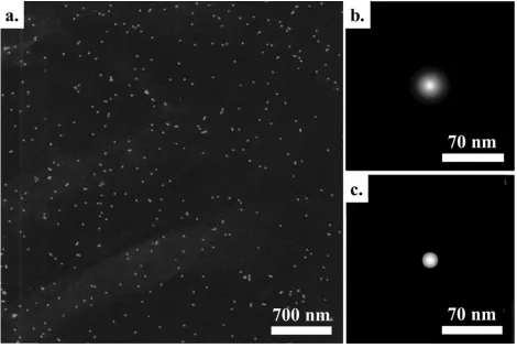
Figure 3-1. Example Calibration Image with Extracted Stacked Particle and Theoretically Calculated Particle. (a) The calibration image taken with a TESCAN VEGA® LaB6 SEM, probe current = 6.45pA, HV = 20keV, (b) the
[image:35.612.72.542.324.640.2]of particle synthesis, the particles will have a varying range of sizes and shapes. By averaging particles together, the size and shape of the particles will converge to the nominal size and shape that is expected for the distribution and will correlate better with the calculated reference image.
Processing the calibration image to create a stacked particle image was carried out using an Aura computer system from Nanojehm, Inc. Selecting particles for stacking is a semi-automated procedure carried out on the basis of particle size and shape. The procedure is referred to as semi-automated in that, if desired, the user has various options to aid in selecting the most representative particles. These options include image smoothing, applying a circularity index, and selecting portions of particles for stacking using an interactive histogram of particle sizes. In the histogram, the peak of the distribution is often near the nominal particle size, but the peak can be shifted away from the nominal size depending on the chosen measurement criteria and the degree of blurring from the convolution. The user should select the region containing the peak because it is the mode of the sizes reported, which corresponds to the nominal size of the particles. Any deviation from the expected size mode is attributed to the PSF, and therefore, those particles representing the mode shift should be used to generate the stacked particle.
3.2.3
Reference Image Generation
Since the particle size and shape is known, a noise-free reference particle image (Figure 3-1c) can be generated by aMonte Carlo simulation program such as CASINO 3D which was used here. The reference particle simulation takes into account the particle size, shape, and composition; the substrate thickness, shape, and composition; and the image generated can be either BSE or SE. In order to obtain a high-resolution image, the probe size was set at 0.1nm for the simulation.
3.2.4
The PSF Calculation and Visualization
The relationship between the measured image (i.e., 2D matrix) of the standard 𝐼𝑂(𝑖, 𝑗) and the true image 𝐼𝑇(𝑖, 𝑗) is given by:
𝐼𝑂(𝑖, 𝑗) = 𝑃𝑆𝐹(𝑘, 𝑙) ⊗ 𝐼𝑇(𝑖, 𝑗) + 𝜂(𝑖, 𝑗) (3.1)
where ⊗ is the convolution operator, (𝑖, 𝑗) denotes the coordinates of a specific pixel, and (𝑘, 𝑙)
characterized by noise associated with electron emission statistics and scattering, an additional term 𝜂(𝑖, 𝑗) is added which denotes the noise contributions to the signal at location (𝑖, 𝑗).
Wiener deconvolution is one method of PSF determination, which uses the stacked particle image along with the theoretically determined reference image. The Wiener method involves taking the Fourier transform of Equation 3.1 to simplify the problem by replacing the convolution operation (spatial domain) with multiplication (frequency domain). This process and the following mathematics are described in detail by Gonzalez & Woods (2009). Prior to the Fourier transform, the PSF is padded with zeros to the same dimension as 𝐼𝑂(𝑖, 𝑗), 𝐼𝑇(𝑖, 𝑗), and 𝜂(𝑖, 𝑗). The Fourier Transform of the PSF is the optical transfer function (OTF), which describes the spatial frequencies that pass through the imaging system. Therefore, Equation 3.1 can be reformulated as the following:
𝑂(𝑢, 𝑣) = 𝑂𝑇𝐹(𝑢, 𝑣) ∙ 𝑇(𝑢, 𝑣) + 𝑁(𝑢, 𝑣) (3.2)
where 𝑂 is the transform of the observed image, 𝑂𝑇𝐹 is the optical transfer function, 𝑇 is the transform of the true image, and 𝑁 is the Fourier representation of the noise. The coordinates (𝑢, 𝑣)
are in spatial frequency units. Since spatial frequency is not always easy to understand, consider a series of parallel lines such as in a microelectronic device that are 10nm apart. The spatial frequency is 0.1 lines per nanometer. As the lines become closer their spatial frequency increases. Considering the noiseless case where 𝑁 = 0, Equation 3.2 can be rearranged to give an estimate of the PSF:
𝑃𝑆𝐹̂ (𝑘, 𝑙) = 𝐹−1[𝑂𝑇𝐹(𝑢, 𝑣)] = 𝐹−1[𝑂(𝑢, 𝑣)
𝑇(𝑢, 𝑣)] (3.3)
However, it is well known that in most situations there are values in 𝑇(𝑢, 𝑣) that are either zero or close to zero. In practice, this leads to the equivalent of division by zero which is an undefined behavior.
𝑃𝑆𝐹̂ (𝑘, 𝑙) = 𝐹−1[[ 𝑇
∗(𝑢, 𝑣)
|𝑇(𝑢, 𝑣)|2+ 𝑆
𝑁(𝑢, 𝑣) 𝑆⁄ 𝑂𝑇𝐹(𝑢, 𝑣)
] 𝑂(𝑢, 𝑣)] (3.4)
where:
𝑇∗(𝑢, 𝑣) = complex conjugate of 𝑇(𝑢, 𝑣)
|𝑇(𝑢, 𝑣)|2 = 𝑇(𝑢, 𝑣)𝑇∗(𝑢, 𝑣)
𝑆𝑁(𝑢, 𝑣) = |𝑁(𝑢, 𝑣)|2= power spectrum of the noise
𝑆𝑂𝑇𝐹(𝑢, 𝑣) = |𝑂𝑇𝐹(𝑢, 𝑣)|2 = power spectrum of the OTF
Notice that in situations where there is no noise or where the SNR is sufficiently high (𝑆𝑁(𝑢, 𝑣) → 0 or 𝑆𝑂𝑇𝐹(𝑢, 𝑣) → ∞), then the noise-to-OTF term drops out and Equation 3.4 reduces to the inverse filter given in Equation 3.3.
Since neither the power spectrum of the noise nor the power spectrum of the signal can be precisely known in practice, 𝑆𝑁(𝑢, 𝑣) 𝑆⁄ 𝑂𝑇𝐹(𝑢, 𝑣) is traditionally replaced and estimated by
𝐾 = 𝑆𝑁(𝑢, 𝑣)
𝑆𝑂𝑇𝐹(𝑢, 𝑣) (3.5)
reducing Equation 3.4 to the following:
𝑃𝑆𝐹̂ (𝑘, 𝑙) = 𝐹−1[[ 𝑇 ∗(𝑢, 𝑣)
|𝑇(𝑢, 𝑣)|2+ 𝐾] 𝑂(𝑢, 𝑣)] (3.6)
where K is a constant added to each value in |𝑇(𝑢, 𝑣)|2 and is chosen such that sufficient
compensation is made for the noise in the images. As the noise increases, K must increase to effectively regularize the noise in the result. If the noise in the stacked particle image is minimal,
3.3
Results and Discussion
3.3.1
Calibration Robustness and the Effect of Beam Energy
A variety of experiments were performed to test the robustness and validity of the method for PSF determination described here. One approach to robustness is to see if different fields of nanoparticles on a calibration sample produce the same PSF, which is expected if the beam is unchanged between images. It should be noted that even when the beam is unchanged, the PSF is changing at each pixel due to the stochastic nature of electron emission. This method determines an average PSF over the field, which may be good enough for probe size measurement and other applications.
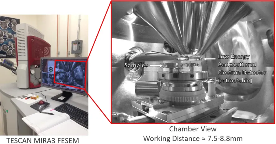
To test calibration robustness, six different regions of nanoparticles were imaged on a calibration sample (Figure 3-4). BSE images were collected at 2kV, 3kV, 4kV, 5kV, 10kV, and 20kV on a TESCAN MIRA3. The samples were situated at a WD of ~7.5-8.8mm using stage
Figure 3-2. PSF Display Modes. a: top-down image, b: surface plot, and c: contour map. Color scale indicates intensity from 0 to 1.
Figure 3-3. Example of PSF Variations with K Value Selection. The largest K that gives a smoothly varying and monotonically decreasing value as a function of distance from the center is optimal (K = 3162 in this case). Inner Contour (red): 0.9Imax, Middle Contour (green): 0.5Imax, Outer Contour (blue): 0.1Imax, where Imax is the maximum
height control. The minimum probe size was determined by the microscope software which resulted in probe currents ranging from about 75pA to 205pA depending on the beam voltage.
At each voltage, six regions were imaged within an area equal to one 42μm x 42μm TEM grid square. The six regions were imaged using the same beam shape to test calibration robustness and repeatability, meaning no changes were made to the focus using beam parameters once the best focus image was collected. The best focus was found for the first region by making typical adjustments to the beam (using focus, stigmators, and wobbler to center the beam). The same magnification was used for the remaining five regions, with occasional changes to stage height to account for variations in sample surface height. This ensured a constant WD. PSFs were then calculated for each region using a Nanojehm Aura workstation which has all the needed software for the abovementioned calculations. The results are presented in Figure 3-5.
As a null case, six images of the same region were captured at 2kV. Small compensations were made to brightness and contrast between images to account for changes in the sample surface as it received more beam exposure. These images were also captured in BSE mode, which reduced the effects of contamination on the image. In SE images, small amounts of contaminaton can cause
the particles to appear larger, and there is a larger background signal from the support film. In BSE images, these concerns are mitigated.
Traditionally, a well-focused SEM electron probe is approximated as a Gaussian (Reimer, 1998). The probe size can then be conveniently characterized using the full width at half maximum (FWHM) which is the dimension that contains 50% of the probe current, and the full width at tenth maximum (FWTM) that contains 90% percent of the probe current.
A Gaussian fit for the determined PSF was tested against Lorentzian, Airy, and sinc function fits, with a single PSF at each 2kV, 5kV, 10kV, and 20kV. The goodness of these fits were compared using sum of squared error, root-mean-square error, and R2. Overall, the Gaussian Figure 3-5. Regional PSF Contours. The 10kV through 2kV plots show overlaid PSF contours of six different nanoparticle fields on the same sample. The 2kV* (null case) plot shows overlaid PSF contours taken of the same nanoparticle field imaged six times. The 2kV and 2kV* data were collected on different dates with different beam shapes, which is why their PSF shapes differ somewhat when compared to each other. In each plot, the inner ring corresponds to 0.5Imax and the outer ring to ~0.1Imax, where Imax is the maximum intensity for a PSF. The first region
produced the best fit for the tested beam voltages, with the Lorentzian matching performance at 2kV. For consistency and simplicity, we used the Gaussian fit to compare PSFs based on their FWHMs as shown in Table 3-1. See Appendix A2 for more detail on use of Gaussians.
As the beam voltage decreased, the minimum probe size increased, which is reflected in the behavior of the PSFs. Decreasing beam voltage also introduced more noise into the PSFs. More pixels are required to define the size and shape of the PSF as the beam size increases. This effect coupled with lower beam current at lower voltages results in reduced signal at each pixel, making the PSF is more susceptible to noise.
The 2kV data and 2kV* (null case) data were taken at different times. Efforts were made to use the same operating conditions between data collections. An important difference between collections remained: the 2kV calibration fields were much sparser in terms of the nanoparticle dispersion compared to the 2kV* data. Less particles to stack means less average signal and poorer counting statistics. When compared to the 2kV* (null case) data, this could account for the increased amount of noise in the 2kV data.
While the 3kV beams’ best focus and astigmatism might have been improved to produce more circular beam footprints, the required changes would be subtle and do not affect the conclusions. Notably, even if the shape was not optimal, each region of nanoparticles produced the same PSF, respectively for each beam energy.
Table 3-1. Regional PSF FWHMs.
Axis Distribution of FWHMs [nm]
a
20kV 10kV 5kV 4kV 3kV 2kV 2kV*b x 10.5 ± 0.2 11.1 ± 0.2 14.5 ± 0.5 15.0 ± 0.5 19.4 ± 0.5 24.2 ± 0.8 30.2 ± 0.8
y 10.9 ± 0.4 11.2 ± 0.2 14.2 ± 0.2 15.2 ± 0.3 16.7 ± 0.8 28.7 ± 1.3 30.9 ± 0.9
aEach entry is the mean ± one standard deviation of the six FWHMs calculated from the PSFs for that voltage and
axis. These FWHMs were calculated using PSFs determined with K = 1000.
3.3.2
Comparison of the New Method with the Knife Edge Test
As mentioned previously, the knife edge test has become a fairly standard way of measuring the PSF. A scan across a knife edge produces a profile plot that has the form of an error function if the PSF is Gaussian. The differentiation of the profile will lead directly to a one dimensional PSF curve in the direction of the scan. If the curve is radially symmetric, then it can be described by a single scan. If not, multiple scans are required over a range of directions to determine a two-dimensional PSF, which can be rather time consuming. In practice, the FWHM is determined by first finding the distance between x-axis values corresponding to the locations of 25% and 75% of the full profile intensity (𝑑25%−75%) obtained from the beam being completely on or off the knife edge depending on whether a signal is measured above the knife edge (SE or BSE) or below it (transmitted). The FWHM is then calculated from (Kološová et al., 2015):
𝑑25%−75%= 0.57𝑑𝐹𝑊𝐻𝑀 (3.7)
A derivation confirming Equation 3.7 is shown in Appendix B.1.
The knife edge method and the previously described new method were compared using BSE data obtained from an EMS 79510-01 gold-on-carbon standard for the knife edge measurements and 18.2nm gold particles on a carbon film for the new method. At each tested beam energy, the particles and the gold-on-carbon standard were imaged with the same beam shape. Ten different profiles at various angles (perpendicular to a feature edge) were measured on gold-on-carbon features. The ImageJ plugin GaussFit (Schneider et al., 2012) was used to determine
𝑑25%−75% for each profile. The same ten angles were used to measure profiles of the corresponding
Table 3-2. Comparison of FWHM Determined by Knife Edge Measurement and the New Method.
Beam Energy
[keV]a
GaussFit
FWHM [nm]b
New Method
FWHM [nm]b
2 22.8 ± 1.5 20.8 ± 1.7
5 13.9 ± 1.7 13.5 ± 0.9
10 10.8 ± 1.4 9.7 ± 0.9
20 8.8 ± 0.8 10.2 ± 1.0
aImages were captured using typical operating conditions for a Schottky source instrument.
PSF (K = 1000), determined from the particle image. Gaussians were fitted to the profiles in MATLAB, from which the FWHM could be calculated.
Table 3-2 summarizes the FWHM comparison of the two methods. The agreement is sufficiently close to indicate that the two methods give similar results with subtle differences, possibly due to factors such as the sample not being a perfect knife edge or the selection of the K
parameter.
3.3.3
Effect of Working Distance
WD is defined as the distance between the bottom of the final lens and the sample. Shorter WDs are related to higher resolution because smaller probe sizes are achievable as a result of reduced aberrations and greater source demagnification.
To study the effect of WD, calibration images were collected over a range of WDs at 2kV, 10kV, and 20kV using a Schottky field emission source on the MIRA3. For each WD, the sample’s z-axis position was altered and the beam refocused. The calibration standard consisted of 18.2nm gold spheres (measured by TEM) on a thin carbon film, similar to other measurements described above. The probe current was held constant for all WDs at a particular voltage.
The PSF size increases as WD increases at all voltages, which matches the expected behavior of the beam size. FWHM contours at 2kV and average values are shown in Table 3-3 and Figure 3-6, respectively. FWHM contours at 10kV and 20kV are included in Appendix B.2.
Table 3-3. Working Distance Series Average FWHMs for Tested Voltages.
WD [mm] Average PSF FWHM [nm]
a
2kV 10kV 20kV 8 22.0 ± 0.1 11.8 ± 0.1 10.8 ± 0.1
12 23.4 ± 0.1 12.5 ± 0.1 11.3 ± 0.1
16 27.4 ± 0.1 13.2 ± 0.1 11.7 ± 0.1
20 31.7 ± 0.1 14.1 ± 0.1 11.9 ± 0.1
24 34.6 ± 0.2 13.9 ± 0.1 12.3 ± 0.1
aThe average FWHM was determined from the FWHM values in the x- and y-direction. The uncertainty shown is
The effect of WD was also used to evaluate the PSF above and below the best focus condition. This resulted in a cross-sectional look at the 3D shape of the electron beam, which is included in Appendix B.2.
3.3.4
Characterization of Astigmatism
Astigmatism is an aberration related to different focal lengths found on perpendicular intersecting planes parallel to and containing the optical axis of an electron optical system. Detailed descriptions can be found in a number of sources including Khursheed (2011) and Klemperer and Barnett (2011). When present, a circular object may appear as: 1) an ellipse in an image plane short of the desired WD, 2) a circle at the WD, and 3) a rotated ellipse in a plane beyond the WD. Consequently, even at the WD the circle is described as a disk of least confusion which will be larger than what would be obtained in the absence of astigmatism. In SEMs, astigmatism correction is normally done by electromagnets placed in the objective lens that can compensate for uneven focus in perpendicular planes along the optical axis. If left uncorrected, this aberration
distorts the size and shape of the PSF. Sources of astigmatism are poor column alignment, defects in the optics, and contamination.
From an operator’s perspective, astigmatism is one of the most difficult corrections to make since it often involves searching for the sharpest possible image as slight adjustments are made to the compensating field while observing a rapidly-scanned, noisy image. The objective of this phase of the study was to demonstrate that measurement of the PSF can provide information on the relationship between astigmatism settings and the size and shape of the probe at a desired WD and beam energy. This research could lead to a new method for automated astigmatism correction.
PSFs were, therefore, investigated at different beam voltages for various degrees of astigmatism using the method described in this article. At each voltage, a calibration sample of 18.2nm gold nanoparticles on graphene was imaged with each beam shape. Additionally at 10kV, a gold-on-carbon resolution standard (Electron Microscopy Sciences cat. #79510-01) was imaged after the calibration image was collected. The calibration sample images were used for PSF determination, and the gold-on-carbon images were used to visualize the effects of astigmatism on a sample-of-interest, as well as for testing image restoration using PSF deconvolution as will be described in a later section.
To collect an astigmatism series, best focus images and stigmated images of the samples were recorded. The best focus image was captured using standard focusing parameters (i.e., WD, stigmation, and wobbler). Astigmatism was gradually added with one stigmator, while the other stigmator was held constant at the best focus value, and vice versa. Afterwards, a few images were collected where both stigmators were adding astigmatism to the image. Astigmatism series were captured at 2kV, 5kV, 10kV, and 20kV using a Schottky field emission source.
Figure 3-7. Astigmatism Series at 10kV. A box containing a contour plot is shown for each PSF. Each box has size 85nm x 85nm. The contours shown are 0.9Imax (inner contour), 0.5Imax (middle contour), and ~0.1Imax (outer contour),
where Imaxis the maximum intensity for the PSF within the box. Minor artifacts from the PSF determination process
3.3.5
Electron Source Type
To gain insight into how the PSF varies with source type, BSE images of a calibration standard were obtained with Schottky and thermionic source (LaB6) instruments at nearly identical
imaging conditions (i.e., WD and accelerating voltage), specifically at 20kV and WDs close to 9mm. The chosen operating conditions did not necessarily maximize resolution. The measured probe currents were 182.42pA and 6.45pA for the Schottky and LaB6 instruments, respectively.
Figure 3-8 shows the FWHM for both beams. Not surprisingly, the beam for the LaB6 instrument
shows a FWHM almost one-and-a-half times that of the Schottky instrument even though the measured specimen current in the Schottky is orders of magnitude above that of the LaB6.
Additionally, the 6.45pA of current for the LaB6 is spread out over a much larger area than the
Schottky. The PSF images show the current density per square nm. They were obtained by normalizing the PSFs and then multiplying the measured probe current by the normalized PSF matrix to give a map of the current density for the beam cross-sections. Knowledge of the current
density should prove useful for understanding the nature of exposure of resist materials in electron beam lithography.
3.3.6
Image Restoration
Once a PSF is determined (using a calibration image of nanoparticles), any images taken with the same beam shape can be restored. The restoration process described and reviewed previously by Lifshin (2014) is based on Equation 3.1. However, instead of having an observed and reference image pair to determine the PSF, the observed image and the PSF are known and the true image is determined. It is standard practice to recast Equation 3.1 in a stacked vector form where m x n matrices (the observed image, the true image, and the noise) are described by mn x 1
vectors and the PSF is described by an mn x mn block circulant matrix derived from its coordinate dependent coefficients as follows:
𝑏⃗ = 𝑨𝑥 + 𝜂 (3.8)
where 𝑏⃗ is the vectorization of the observed image, 𝑨is the block circulant form of the PSF, 𝑥 is the vectorization of the true image, and 𝜂 is the vectorization of the noise. The determination of the true image requires the solution of this equation. In the absence of noise, Equation 3.3 could be readily solved by multiplying it by the inverse of the 𝑨 matrix, 𝑨−𝟏. However, 𝑨 is highly sensitive to noise, and error can increase when values of 𝑨 are near or equal to zero. The increased error produces an “ill-posed” problem. This means that in trying to solve the inverse problem (going from the observed image to the true image) multiple possible solutions may exist. Only through constraints or penalty terms can the most likely answer be found. A simple example of a constraint is that any solution where the true intensity is less than zero would be unacceptable. Finding a solution to Equation 3.8 involves converting it to a functional minimization problem:
𝑓(𝑥) = 𝑎𝑟𝑔𝑚𝑖𝑛
𝒙
{‖𝑨𝑥 − 𝑏⃗ ‖22+ 𝜆𝑅(𝑥 )} 𝑠. 𝑡. 𝑥 ≽ 0 (3.9)
while minimizing any artifacts introduced during deconvolution. These artifacts can include false background texture, shadows, and ringing.
In theory, PSF deconvolution is able to restore information lost to blur and distortion by the imaging system. This is because PSF deconvolution uses knowledge about how the image was formed. Restoration should be distinguished from image enhancement which does not use this knowledge, but rather modifies the image to accentuate specific features. Example restorations from the 10kV astigmatism series presented in Figure 3-7 can be seen in Figure 3-9. The observed images and corresponding restorations from the entire 10kV series are included in Appendix B.4. Restorations usually took a matter of seconds to perform for n x n images where n = 1024, 2048, or 4096 pixels.
PSF deconvolution was able to restore lost information to the astigmatic images and best focus cases. Qualitatively, the best focus images resulted in the cleanest restorations. As more astigmatism was added to the images, the restorations became less clear and more artifacts were introduced (e.g., ringing, shadowing).
[image:50.612.80.533.394.617.2]3.4
Conclusions
Details of a new method for determining the point spread function (PSF) of an SEM have been presented and shown to be consistent with commonly used knife edge methods. The advantage of this new method is not only speed, since it requires only a single measurement for the determination of the two-dimensional PSF, but also no assumptions need to be made about the shape of PSF which can be highly non-symmetrical about the beam axis. A variety of uses for the PSF were presented, including measuring astigmatism, quantifying the effect of experimental factors such as WD and beam energy, and improving SEM image resolution and quality through deconvolution and regularization.
While the presented results show clear benefits of using this method, additional research can lead to improvement and further understanding. The PSF is a mathematical bridge between a true image (the image of an object not subjected to distortion, noise, or any limitation to spatial resolution) and the image observed with an SEM. It is difficult, however, to fully understand how the standard used to measure the PSF may affect the result. For example, in the case of a knife edge experiment using SE, artifacts may result from lateral edge emission when the beam is near the edge of a particle or feature. This problem may also influence the results of the new method, but the degree of this effect has not yet been determined for either method. Lateral edge emission becomes more serious as beams become smaller and smaller. Edge emission (i.e., edge brightening) when imaging with SE is investigated as part of Chapter 4.
On one level, the PSF may be thought of as the spatial distribution of electrons in the plane of focus p