ANALYSIS ON THE ROBOTICS CHIP MOUNTER
PERFORMANCE
NORKHUZAIMAH BT AB.KADIR
B051110336
UNIVERSITI TEKNIKAL MALAYSIA MELAKA
UNIVERSITI TEKNIKAL MALAYSIA MELAKA
ANALYSIS ON THE ROBOTICS CHIP MOUNTER
PERFORMANCE
This report submitted in accordance with requirement of the Universiti Teknikal Malaysia Melaka (UTeM) for the Bachelor Degree of Manufacturing Engineering
(Robotics & Automation) (Hons.)
by
NORKHUZAIMAH BINTI AB.KADIR
B051110336
830624-03-5934
UNIVERSITI TEKNIKAL MALAYSIA MELAKA
BORANG PENGESAHAN STATUS LAPORAN PROJEK SARJANA MUDA
TAJUK: ANALYSIS ON THE ROBOTICS CHIP MOUNTER PERFORMANCE
SESI PENGAJIAN: 2013/14 Semester 2
Saya NORKHUZAIMAH BINTI AB.KADIR
mengaku membenarkan Laporan PSM ini disimpan di Perpustakaan Universiti Teknikal Malaysia Melaka (UTeM) dengan syarat-syarat kegunaan seperti berikut: 1. Laporan PSM adalah hak milik Universiti Teknikal Malaysia Melaka dan penulis. 2. Perpustakaan Universiti Teknikal Malaysia Melaka dibenarkan membuat salinan
untuk tujuan pengajian sahaja dengan izin penulis.
3. Perpustakaan dibenarkan membuat salinan laporan PSM ini sebagai bahan pertukaran antara institusi pengajian tinggi.
4. **Sila tandakan (√)
SULIT
TERHAD
TIDAK TERHAD
(Mengandungi maklumat yang berdarjah keselamatan atau kepentingan Malaysiasebagaimana yang termaktub dalam AKTA RAHSIA RASMI 1972)
(Mengandungi maklumat TERHAD yang telah ditentukan oleh organisasi/badan di mana penyelidikan dijalankan)
Alamat Tetap:
No.277, Kg. Gajah Mati, 16400 Melor,
Kota Bharu, Kelantan.
Tarikh: _________________________
Disahkan oleh:
Cop Rasmi:
Tarikh: _______________________
DECLARATION
I hereby, declared this report entitled “Analysis on the Robotics Chip Mounter Performance” is the results of my own research except as cited in references.
Signature : ……….
Author’s Name : NORKHUZAIMAH BT AB. KADIR
APPROVAL
This report is submitted to the Faculty of Manufacturing Engineering of UTeM as a partial fulfillment of the requirements for the degree of Bachelor of Manufacturing Engineering (Robotics & Automation) (Hons.). The member of the supervisory committee is as follow:
……… Supervisor,
Dr. Fairul Azni b Jafar
i
ABSTRAK
ii
Ishikawa (diagram tulang ikan). Analisis turut dibuat dengan mengkaji tenaga kerja,
iii
ABSTRACT
iv
v
DEDICATION
For my mother Siti Eshah bt Abdullah and my beloved family, Their loving and unconditional support throughout my life. Without whose love and supported this may not be completed.
vi
ACKNOWLEDGEMENT
First and foremost I would like to express my sincere gratitude to Universiti Teknikal Malaysia Melaka (UTeM) particularly School of Manufacturing Engineering (Robotics & Automation) for giving me a great opportunity to handle great project. It would be a great learning process experience in research the information and knowledge about the subject study. These valuable experiences also convince students to face the real situation after graduation.
vii
TABLE OF CONTENT
Abstrak i
Abstract iii
Dedication v
Acknowledgement iv
Table of Content vii
List of Figures x
List of Tables xiii
List Abbreviations xiv
CHAPTER 1: INTRODUCTION 1
1.1 Background 1
1.2 Motivation 3
1.3 Problem Statement 3
1.4 Objective 3
1.5 Scope 4
1.6 Report Structure 4
CHAPTER 2: LITERATURE REVIEW 5
2.1 Introduction 5
2.1.1 Chip Mounter Machine 6
viii
2.2 Problem of Chip Mounter 11
2.2.1 Unstable Production Time 14
2.2.2 Product Defect 15
2.3 Problem Analysis Method 16
2.4 Summary 19
CHAPTER 3: METHODOLOGY 20
3.1 Introduction 20
3.2 Planning 21
3.2.1 Identify Problem 22
3.2.2 Understand Problem 22
3.2.3 Review Problem 23
3.3 Design of Experiment (DOE) 23
3.3.1 Measurement of Production Time 25
3.4 Analysis Method 27
3.4.1 Man 27
3.4.2 Machine 27
3.4.2.1 Nozzle Investigation 28
3.4.3 Material 29
3.4.3.1 Component Checking 29
3.4.4 Method 30
ix
CHAPTER 4: RESULT AND DISCUSSION 32
4.1 Experiment Result- Measurement Data 32
4.2 Analysis Results – Possible Causes 40
4.2.1 Man 41
4.2.2 Machine 41
4.2.2.1 Nozzle 41
4.2.2.2 Vacuum 43
4.2.3 Material 45
4.2.3.1 Component 45
4.2.3.2 Casing 49
4.2.4 Method 51
4.3 Suggestion for Counter Measure 51
4.3.1 Design of Vision System 52
4.4 Summary 56
CHAPTER 5: CONCLUSION AND RECOMMENDATIONS 57
5.1 Conclusion 57
5.2 Recommendation 58
REFERENCES 59
x
LIST OF FIGURES
1.1 Example of printed circuit board 2
2.1 Example of mounter machine 7
2.2 A chip mounter with single head 8
2.3 Example configuration of a chip mounter machine 9
2.4 PCBtables in x-direction and y-direction 10
2.5 Pick and place surface mount machine 11
2.6 Feeder rack 13
2.7 Assemblying component on PCB 14
2.8 Surface mount electronic component feeder for use in a robotic pick-and-place SMT machine 15
2.9 Nozzle chip mounter machine 16
2.10 Placement component on PCB board 17
2.11 Component in reel tape 18
3.1 Overall flowchart of the project 22
3.2 Flowchart of the project planning 23
3.3 Flowchart of design of experiment (DOE) process 25
3.4 Flowchart of the production time measurement process 25
xi
3.7 Measure component length 34
4.1 Sample of PCB with 34 comonents 37
4.2 Example type of nozzle 46
4.3 Types of nozzle 46
4.4 Top of the nozzle 47
4.5 Types of nozzle 47
4.6 Vacuum head on process chip mount 48
4.7 Vacuum head on nozzle head 48
4.8 Inductor used in the chip mount process 49
4.9 Inductor in reel 50
4.10 Resistor 50
4.11 Resistor diagram 51
4.12 Resistor in reel 51
4.13 Capasitor 52
4.14 Capasitor in reel 52
4.15 Casing of inductor 53
4.16 Missing component on PCB 54
4.17 Casing of resistor 54
4.18 Various types of casing component 54
xii
4.21 Arm robot with vision solid-state 58
4.22 Application camera solid state inside chip mounter machine 58
4.23 Arm robot with vision vidicon 59
xiii
LIST OF TABLES
3.1 Data time by strips. 26
3.2 Data time for by sublots 27
4.1 Time for PCB with 34 components 37
4.2 Time for PCB with 33 components 38
4.3 Time for PCB with 30 components 39
4.4 Time for PCB with 22 components 40
4.5 Time for PCB with 14 components 41
4.6 Time for PCB with 18 components 41
4.7 Time for PCB with 10 components 42
4.8 Time for PCB with 9 components 43
4.9 Time for PCB with 8 components 43
xiv
LIST OF ABBREVIATIONS
PCB - Printed Circuit Board SMT - Surface Mount Technology DOE - Design of Experiment
FAP - Feeder Arrangement Problem PSP - Placement Sequencing Problem TSP - Travelling Salesmen Problem NP - Non-Polynomial
QAP - Quadratic Assignment Problem PSO - Particle Swarm Optimization FMS - Flexible Manufacturing System DC - Direct Current
1
CHAPTER 1
INTRODUCTION
1.1 Background
Development of electronic industry is blooming in line with the development. Increased use of electronics to go global. The industry is getting fierce competition among manufacturers of electronic products. Sophiscated electronic to expand as a technology advanced era. Customer demand increased, then the development of technology production system to be effective and productive.
2
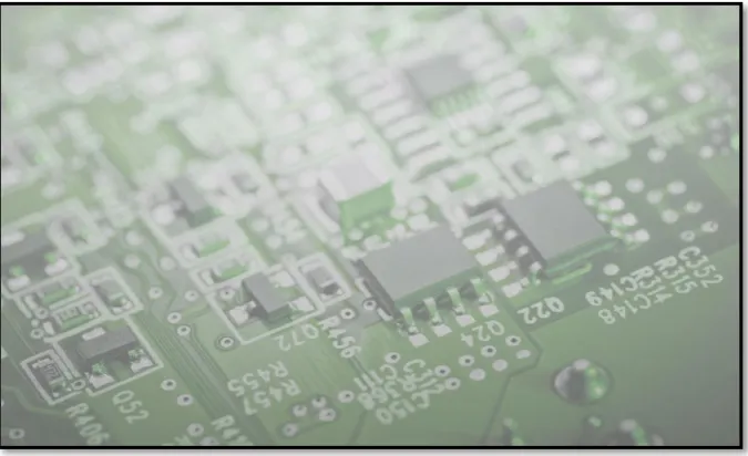
Figure 1.1: Example of Printed Circuit Board.
(Source: < http://www.dreamstime.com/royalty-free-stock-photography-pcb-printed-circuit-board-3d-image14007547 >25/09/2013)
The assembly of PCBs is a complex task since a PCB may contain hundreds of electronic components in different shapes and sizes mounted at specific locations on the substrate. In the past, substrate assembly consist of inserting leads through holes in the board and then solder them into the place. Currently, Surface Mount Technology (SMT) is generally used in PCBs assembly. With SMT, components are attached to a bare substrade with solder paste at pre specified location. Then a reflow operation heats the substrade causing the solder paste to melt for the proper connections.
The beginning of process for surface mount technology is substrade bake that heat substrade from water vapour for about 5 hours. Solder paste will be wiped in stencil that was punched according to substrade size. Next is the process of chip mounting, where components are mounted in substrade or PCBs.
3
1.2 Motivation
Chip mounter is important in the process of SMT. In semiconductor industry, Integrated Circuit (IC) must be mounted and for that chip mounter machine is widely employed. In many cases, defect found on PCB analysis on the chip mounter machine is required in order to reduce defect in PCB and indirectly reduce cost of losses and increase product quality.
1.3 Problem Statement
Efficiency in chip mounter machine movement in terms of nozzle and system for mounting component on PCBs, indeed was acknowledged. Time efficiencies in chip mounter machine used is not accordance to the time of system process for mounting component in substrade. Nozzle is important to be efficiently moved for chip mounter when carrying out the process.
In many SMT industries, there are defects in PCBs which caused by component missing and component misalignment. Defect which occured will reduce PCBs quality for customer satisfaction.
1.4 Objective
The objectives of this project are :
i. To identify the cause of unstable production time and product defect on PCB assembly process.
4
1.5 Scope
The scopes of this project will emphasis on conducting experimental analysis : i. Analysis on chip mounter machine is for one line selected which always
come out with operational performance problems and product defect. ii. The study involve several type of PCBs mounted in the selected production
line.
1.6 Report Structure
This report is structured as follows :
Chapter 1 explain the introduction of chip mounter machine that efficient and quick in mounting component process and defect that happened in PCBs.
Chapter 2 consists of literature review study which describes the related works of chip mounter machine for industrial.
Chapter 3 describes the methodology used in this study including the overall flow chart the project.
Chapter 4 present the result and discussion on the chip mounter performances.
Chapter 5 is the conclusion that concludes the project by presenting the final outcome and achievement as well as future recommended works.
5
CHAPTER 2
LITERATURE REVIEW
This report is focusing on the chip mounter performances in SMT field. Section 2.1 of this report will explain in the introduction of chip mounter, section 2.2 will discuss about problem in process chip mounter, section 2.3 will explore methods use for optimization of chip mounter and 2.4 summary of this report.
2.1 Introduction