Erbium-doped glass nanoparticle embedded
polymer thin films using femtosecond pulsed
laser deposition
E
RICK
UMIB
ARIMAH,
1,*M
ARCINW. Z
IARKO,
2N
IKOLAOSB
AMIEDAKIS,
2I
ANH. W
HITE,
2R
ICHARDV. P
ENTY,
2ANDG
INJ
OSE11School of Chemical and Process Engineering, University of Leeds, Clarendon Road, Leeds LS2 9JT, UK
2Centre for Photonic Systems, Department of Engineering, University of Cambridge, 9 J. J. Thomson Ave, Cambridge CB3 0FA, UK
*preeku@leeds.ac.uk
Abstract: Polymer materials doped with rare-earth ions are promising candidates for the formation of low-cost integrated optical amplifiers. However, there are significant technical challenges associated with the integration of these dissimilar materials and the formation of high-quality Er-doped polymer films. In this paper, therefore, we present for the first time the fabrication of polymer thin layers modified with erbium-doped sodium zinc tellurite (Er-TZN) glass nanoparticles (NPs) using femtosecond (fs) pulsed laser deposition (PLD) and the characterisation of their basic properties. The surface morphology and the compositional and structural characteristics of the samples produced with this method are evaluated using scanning and transmission electron microscopy (SEM and TEM) and X-ray diffraction (XRD), while photoluminescence (PL) measurements are carried out at room temperature under a 980 nm laser diode excitation. The studies indicate that the Er-doped TZN NPs are successfully integrated in the polymer layers. The obtained average NP size is measured to be in the range of 12 to 21 nm depending on the fabrication parameters, while broad PL emission at 1534 nm that corresponds to the 4I
13/2 →4I15/2 transition of Er3+ is observed from the
samples. The full-width at half-maximum (FWHM) of the PL spectra is found to be ~39 nm while the fluorescence lifetime is measured to be in the range of 3.52 to 4.18 ms. The obtained results clearly demonstrate the potential to efficiently dope polymer layers with glass NPs using fs-PLD and is a first step towards the successful formation of hybrid polymer-glass waveguide amplifiers.
Published by The Optical Society under the terms of the Creative Commons Attribution 4.0 License. Further distribution of this work must maintain attribution to the author(s) and the published article’s title, journal citation, and DOI.
OCIS codes: (130.5460) Polymer waveguides; (160.4236) Nanomaterials; (160.4760) Optical properties; (310.0310) Thin films; (300.0300) Spectroscopy.
References and links
1. Z. Zhao, G. Jose, P. Steenson, N. Bamiedakis, R. V. Penty, I. H. White, and A. Jha, “Tellurite glass thin films on silica and polymer using UV (193 nm) pulsed laser ablation,” J. Phys. D Appl. Phys. 44(9), 095501 (2011). 2. C. E. Brunchi, A. Filimon, M. Cazacu, and S. Ioan, “Properties of some poly(siloxane)s for optical applications,”
High Perform. Polym. 21(1), 31–47 (2009).
3. V. Prajzler, P. R. Mastera, and P. Nekvindova, “Properties of siloxane based optical waveguides deposited on transparent paper and foil,” Wuxiandian Gongcheng 25(2), 230 (2016).
4. H. Ma, A. K.-Y. Jen, and L. R. Dalton, “Polymer-based optical waveguides: materials, processing, and device,” Adv. Mater. 14(19), 1339–1365 (2002).
5. R. S. E. John, C. M. Amb, B. W. Swatowski, W. K. Weidner, M. Halter, T. Lamprecht, and F. Betschon, “Thermally stable, low loss optical silicones: a key enabler for electro-optical printed circuit boards,” J. Lightw. Tech. 33(4), 814–819 (2015).
6. E. Zgraggen, I. M. Soganci, F. Horst, A. La Porta, R. Dangel, B. J. Offrein, S. A. Snow, J. K. Young, B. W. Swatowski, C. M. Amb, O. Scholder, R. Broennimann, U. Sennhauser, and G.-L. Bona, “Laser direct writing of single-mode polysiloxane optical waveguides and devices,” J. Lightw. Tech. 32, 814 (2015).
#328268 https://doi.org/10.1364/OME.8.001997
7. J. C. Dingeldein, K. A. Walczak, B. W. Swatowski, C. R. Friedrich, C. T. Middlebrook, and M. C. Roggemann, “Process characterization for direct dispense fabrication of polymer optical multi-mode waveguides,” J. Micromech. Microeng. 23(7), 075015 (2013).
8. R. Dangel, F. Horst, D. Jubin, N. Meier, J. Weiss, B. J. Offrein, B. W. Swatowski, C. M. Amb, D. J. DeShazer, and W. K. Weidner, “Development of versatile polymer waveguide flex technology for use in optical interconnectsm,” J. Lightw. Tech. 31(24), 3915–3926 (2013).
9. N. Bamiedakis, A. Hashim, R. V. Penty, and I. H. White, “A 40 Gb/s optical bus for optical backplane interconnections,” J. Lightw. Tech. 32(8), 1526–1537 (2014).
10. J. Beals, N. Bamiedakis, A. Wonfor, R. Penty, I. White, J. DeGroot, K. Hueston, T. Clapp, and M. Glick, “A terabit capacity passive polymer optical backplane based on a novel meshed waveguide architecture,” Appl. Phys., A Mater. Sci. Process. 95(4), 983–988 (2009).
11. R. C. A. Pitwon, W. Kai, J. Graham-Jones, I. Papakonstantinou, H. Baghsiahi, B. J. Offrein, R. Dangel, D. Milward, and D. R. Selviah, “FirstLight: pluggable optical interconnect technologies for polymeric electro-optical printed circuit boards in data centers,” J. Lightw. Tech. 30(21), 3316–3329 (2012).
12. M. Immonen, R. Zhang, M. Press, H. Tang, W. Lei, J. Wu, H. J. Yan, L. X. Zhu, and M. Serbay, “End-to-end optical 25Gb/s link demonstrator with embedded waveguides, 90° out-of-plane connector and on-board optical transceivers,” in 42nd European Conference on Optical Communication (ECOC) (2016). 1–3.
13. G. A. Kumar, C. W. Chen, R. Riman, S. Chen, D. Smith, and J. Ballato, “Optical properties of a transparent CaF2:Er3+ fluoropolymer nanocomposite,” Appl. Phys. Lett. 86(24), 241105 (2005).
14. L. H. Slooff, A. Polman, M. P. Oude Wolbers, F. C. J. M. V. Veggel, D. N. Reinhoudt, and J. W. Hofstraat, “Optical properties of erbium-doped organic polydentate cage complexes,” J. Appl. Phys. 83(1), 497–503 (1998).
15. M. Zhang, W. Zhang, F. Wang, D. Zhao, C. Qu, X. Wang, Y. Yi, E. Cassan, and D. Zhang, “High-gain polymer optical waveguide amplifiers based on core-shell NaYF4/NaLuF4: Yb3+, Er3+ NPs-PMMA covalent-linking
nanocomposites,” Sci. Rep. 6(1), 36729 (2016).
16. X. Zhai, J. Li, S. Liu, X. Liu, D. Zhao, F. Wang, D. Zhang, G. Qin, and W. Qin, “Enhancement of 1.53 μm emission band in NaYF4:Er3+,Yb3+,Ce3+ nanocrystals for polymer-based optical waveguide amplifiers,” Opt.
Mater. Express 3(2), 270 (2013).
17. T. Kakkar, N. Bamiedakis, T. T. Fernandez, Z. Zhao, M. Irannejad, P. Steenson, A. Jha, R. Penty, I. White, and G. Jose, “Glass–polymer superlattice for integrated optics,” Opt. Eng. 53(7), 071818 (2014).
18. S. Ghatrehsamani and G. E. Town, “Optical gain in polymer composite materials with P2O2: Er3+/Yb3+- codoped
nanoparticles,” J. Quantum Electronics 53(2), 7000705 (2017).
19. Q. Xiang, Y. Zhou, Y. L. Lam, Y. C. Chan, and C. H. Kam, “Deposition and characterization of Er3+ doped, A1
co-doped sol-gel silica films on SOS,” Ferroelectrics 230(1), 55–60 (1999).
20. T. Yada, T. Maejima, MasaruAoki, and M. Umesaki, “Thin-film formation by spin coating: characteristics of a positive photoresist,” Jpn. J. Appl. Phys. 3(1), 6279–6284 (1995).
21. S. C. Hamm, R. Shankaran, V. Korampally, S. Bok, S. Praharaj, G. A. Baker, J. D. Robertson, B. D. Lee, S. Sengupta, K. Gangopadhyay, and S. Gangopadhyay, “Sputter-deposition of silver nanoparticles into ionic liquid as a sacrificial reservoir in antimicrobial organosilicate nanocomposite coatings,” ACS Appl. Mater. Interfaces
4(1), 178–184 (2012).
22. S. Kar, S. Logad, O. P. Choudhary, C. Debnath, S. Verma, and K. S. Bartwal, “Preparation of lithium niobate nanoparticles by high energy ball milling and their characterization,” J. Mater. Sci. 1(2), 18–24 (2013). 23. E. Rebollar, S. Gaspard, M. Oujja, M. M. Villavieja, T. Corrales, P. Bosch, S. Georgiou, and M. Castillejo,
“Pulsed laser deposition of polymers doped with fluorescent molecular sensors,” Appl. Phys., A Mater. Sci. Process. 84(1-2), 171–180 (2006).
24. R. A. Ganeev, U. Chakravarty, P. A. Naik, H. Srivastava, C. Mukherjee, M. K. Tiwari, R. V. Nandedkar, and P. D. Gupta, “Pulsed laser deposition of metal films and nanoparticles in vacuum using subnanosecond laser pulses,” Appl. Opt. 46(8), 1205–1210 (2007).
25. S. Eliezer, N. Eliaz, E. Grossman, D. Fisher, I. Gouzman, Z. Henis, S. Pecker, Y. Horovitz, M. Fraenkel, S. Maman, and Y. Lereah, “Synthesis of nanoparticles with femtosecond laser pulses,” Phys. Rev. B 69(14), 144119 (2004).
26. R. G. Nikov, A. O. Dikovska, N. N. Nedyalkov, G. V. Avdeev, and P. A. Atanasov, “Au nanostructure fabrication by pulsed laser deposition in open air: Influence of the deposition geometry,” Beilstein J. Nanotechnol. 8, 2438–2445 (2017).
27. I. Mirza, G. O’Connell, J. J. Wang, J. G. Lunney, “Comparison of nanosecond and femtosecond pulsed laser deposition of silver nanoparticles films,” Nanotechnology 25, 265301 (2014).
28. J. Chandrappan, M. Murray, P. Petrik, E. Agocs, Z. Zolnai, A. Tempez, S. Legendre, D. P. Steenson, A. Jha, and G. Jose, “Doping silica beyond limits with laser plasma for active photonic materials,” Opt. Mater. Express
5(12), 2849–2861 (2015).
29. J. W. Jeon, S. Yoon, H. W. Choi, J. Kim, D. Farson, S. -H. Cho, “The effect of laser pulse widths on laser-Ag nanoparticle interaction: femto- to-nanosecond lasers,” Appl. Sci. 8, 112–120 (2018).
31. K. Vu and S. Madden, “Tellurium dioxide Erbium doped planar rib waveguide amplifiers with net gain and 2.8 dB/cm internal gain,” Opt. Express 18(18), 19192–19200 (2010).
32. S. Sakida, T. Nanba, and Y. Miura, “Optical properties of Er3+-doped tungsten tellurite glass waveguides by
Ag+-Na+ ion-exchange,” Opt. Mater. 30(4), 586–593 (2007).
33. V. A. G. Rivera, E. F. Chillcce, E. Rodriguez, C. L. Cesar, and L. C. Barbosa, “Planar waveguides by ion exchange in Er3+-doped tellurite glass,” J. Non-Cryst. Solids 352(5), 363–367 (2006).
34. H. Liu, Z. Huang, J. Huang, S. Xu, M. Fang, Y. G. Liu, X. Wu, and S. Zhang, “Morphology controlling method for amorphous silica nanoparticles and jellyfish-like nanowires and their luminescence properties,” Sci. Rep.
6(1), 22459 (2016).
35. V. Koubassov, J. F. Laprise, F. Theberge, E. Forster, R. Sauerbrey, B. Muller, U. Glatzel, and S. L. Chin, “Ultrafast laser-induced melting of glass,” Appl. Phys., A Mater. Sci. Process. 79(3), 499–505 (2004). 36. S. M. Sidel, F. A. Santos, V. O. Gordo, E. Idalgo, A. A. Monteiro, J. C. S. Moraes, and K. Yukimitu, “Avrami
exponent of crystallization in tellurite glasses,” J. Therm. Anal. Calorim. 106(2), 613–618 (2011).
37. M. R. Kasaai, S. Lagace, D. Boudreau, E. Forster, B. Muller, and S. L. Chin, “Creation of micro-holes on glass surface by femtosecond laser through the ejection of molten material,” J. Non-Cryst. Solids 292(1-3), 202–209 (2001).
38. C. Carteret and A. Labrosse, “Vibrational properties of polysiloxanes from dimer to oligomers and polymers, Structural and vibrational properties of hexamethyldisloxane (CH3)3SiOSi (CH3)3,” J. Raman Spectrosc. 41(9),
996–1004 (2010).
39. M. Schmitt, “Analysis of silanes and of siloxanes formation by Raman spectroscopy,” RSC Advances 4(4), 1907–1917 (2014).
40. M. Mazzuca, J. Portier, B. Tanguy, F. Romain, A. Fadli, and S. Turrell, “Raman scattering in tellurium-metal oxyde glasses,” J. Mol. Struct. 349, 413–416 (1995).
41. T. Komatsu, H. Tawarayama, H. Mohri, and K. Matusita, “Properties and crystallization behaviors of TeO2LiNbO3 glasses,” J. Non-Cryst. Solids 135(2–3), 105–113 (1991).
42. K. A. Alim, V. A. Fonoberov, M. Shamsa, and A. A. Balandin, “Micro-Raman investigation of optical phonons in ZnO nanocrystals,” J. Appl. Phys. 97(12), 124313 (2005).
43. D. Yan, P. Wu, S. P. Zhang, L. Liang, F. Yang, Y. L. Pei, and S. Chen, “Assignments of the Raman modes of monoclinic erbium oxide,” J. Appl. Phys. 114(19), 193502 (2013).
44. Y. Jinqiu, C. Lei, H. Huaqiang, Y. Shihong, H. Yunsheng, and W. Hao, “Raman spectra of RE2O3 (RE = Eu, Gd,
Dy, Ho, Er, Tm, Yb, Lu, Sc and Y): laser-excited luminescence and trace impurity analysis,” J. Rare Earths
32(1), 1–4 (2014).
1. Introduction
For the past two decades, several polymer materials such as siloxanes, poly-methyl methacrylates (PMMA), polyimides, acrylates, and olefins resin have been investigated for optical waveguide engineering, ultrafast optical communications, and optical sensing applications [1–4]. Siloxane-based polymers are cost-effective hybrid organic-inorganic materials predominantly consisting of a silicon and oxygen crosslinked network [3], with remarkable thermal, mechanical and optical properties. In particular, they exhibit excellent thermal stability up to at least 300°C prohibiting the yellowing effects that are commonly observed in polymer materials when exposed to temperatures > 100°C. Additionally, they exhibit low absorption in the near-infrared and visible wavelength range, offer good control of its refractive index, and allow direct fabrication onto various rigid or flexible substrates (Si, glass, FR4, polyimidies) [5–8]. As a result, they have been used extensively in recent years to fabricate optical waveguides directly on printed circuit boards and enable the formation of low-cost optical backplanes and board-level optical interconnects [9–12]. However, the waveguides and waveguide components used in such integrated optical circuits are all passive as currently no suitable on-board optical amplification scheme has been demonstrated. The formation of waveguide amplifiers suitable for use in such applications is a major advance that would eliminate the need for optical-to-electrical conversion and electronic amplifiers and enable more sophisticated all-optical interconnections. In this work therefore, we present work towards this goal by developing a method to efficiently integrate Er-doped glass NPs in siloxane polymer films.
Doping polymer materials with rare earth ions has been studied extensively in recent years due to the potential of producing low-cost waveguide amplifiers. The use of polymer matrices modified with Er3+ ions NPs can provide enough isolation between neighbouring ions, and
studies on such rare-earth-modified polymer materials are reported below. Kumar et al. [13] reported on the fabrication and optical properties of CaF: Er3+ nanocrystals doped into a
perfluorocyobutyl-based fluoropolymer composite. A maximum optical gain of 1.78 dB/cm at the 1560 nm wavelength that corresponds to the Er3+ ion transition was obtained. Similarly,
the synthesis and fluorescence properties of an Er-doped organic polydentate cage complex has been reported by Sloff et al. [14]. A FWHM of about 70 nm and a lifetime of 0.8 µs were demonstrated from these composite materials. The paper suggests that the decreased lifetime is due to fluorescence quenching induced by the C-H and O–H groups in the organic polydentate. In addition, various groups have tried to synthesize NaFY4:Er3+: Yb3+ NPs in
PMMA covalent-linking nanocomposites and NaFY4:Er3+,Yb3+, Ce3+ nanocrystals targeting
the formation of polymer-based optical waveguide amplifiers [15-16]. In [15] for example, Zhang et al. synthesized NaYF4/NaLuF4: Yb3+,Er3+ NPs-PMMA covalent-linking
nanocomposites with an optimal concentration ratio of Er3+ to Yb3+ of 1:10, and demonstrated
a net gain of 15.1 dB for a waveguide length of 1.3 cm at 1530 nm. Furthermore, Er3+-doped
tellurite glass-polymer superlattice nanolayers have been produced with nanosecond-pulsed laser deposition (ns-PLD) using a 193-nm ultraviolet laser [17]. The PL spectrum of the samples produced showed a FWHM value of 64 nm and a decay lifetime of 1.8 ms at the Er3+: 4I1
3⁄2 → 4I15⁄2 transition centred at 1534 nm. Recently, Ghatrehsamani et al. using
modelling studies predicted an optical gain of ~15 dB at 1540 nm for an 8 mm long polymer waveguide doped with P2O2: Er3+/Yb3+ NPs of 10 nm radius [18]. These results and the
related intensive research clearly demonstrate that hybrid glass-organic/inorganic nanoparticle thin films are promising candidates for developing high gain Er3+-doped polymer-based
optical waveguide amplifiers.
Several fabrication techniques including sol-gel deposition [19], spin coating [20], sputtering [21], ball milling [22], and ion implantation [23] have been employed to synthesize the inorganic active NPs materials and dope the polymer materials. ns-PLD is a particularly promising method as it allows the production of NPs of different sizes, morphology, and chemical composition by adjusting the laser parameters and chamber conditions. It has been utilized to deposit PMMA, polystyrene, and Er3+-doped tellurite glass on polymer thin films
[1,17]. In recent years, PLD with even shorter pulse duration in the femtosecond range (fs-PLD) has been used to synthesize NPs from several materials such as chromium, stainless steel, indium [24], aluminium [25], and gold (Au) [26]. Through systematic fabrication studies, it has been demonstrated that fs-PLD is more efficient than ns-PLD in generating NPs with equivalent size distributions and preventing NP agglomeration [27]. Additionally, the fs-PLD technique enables the generation of a wider range of NPs sizes by adjusting the energy of the laser pulses and can provide higher doping concentrations without major fluorescence and lifetime quenching [28]. Furthermore, theoretical models have shown that rapid expansion and cooling of the particles ejected from the target by the femtosecond laser could create NPs through various processes such as heterogeneous decomposition, liquid phase ejection and fragmentation, and homogenous nucleation and decomposition [29]. The formation of NPs by using fs-laser is attractive due to the following reasons as compared to nanosecond laser. Firstly, the ejected material does not interact with the subsequent trace of the fs-laser beam, as in the case of ns-laser deposition which then allow the formation of NPs without any external influence. Secondly, the laser-material interactions generate a lot of heat on the target surface without modifying the optical properties of the material, and as a result, the NPs created retain the either amorphous or crystalline property of the target (if the ejected particles size radii are within 1-1000 nm range). However, in the nanosecond region, the size distribution of the NPs becomes broader and clustered, which is disadvantageous for optical sensing and waveguide applications [30]. The ability to embed rare earth doped nanoparticles within a polymer film is the unique feature of fs-PLD used in this study.
ions, and exhibit a broad and strong PL emission at 1534 nm and high amplification gain. For instance, an Er-doped tellurite waveguide has been demonstrated achieving a high gain of 2.8 dB/cm when pumped at 1480 nm [33]. The fabrication of other tellurite-based glass waveguides had been also reported such as TeO2-WO3-Na2O-Er2O3 [32] and TeO2-GeO2
-Na2O-ZnO-Er2O3 [33] with good results. The integration however of Er-doped tellurite NPs
with polymer materials is not straightforward as inorganic salts are not readily soluble in polymers and exhibit large difference in thermal expansion coefficient with common polymer materials [34]. To address this issue, we propose here a new approach of incorporating Er3+-
TZN glass NPs into polymer materials using fs-PLD. The method allows the efficient formation and embedding of NPs with sizes smaller than 40 nm in the polymer layers achieving a high surface area-to-volume ratio and good film uniformity. To the best of our knowledge, this is the first report of the use of fs-PLD for doping siloxane materials with Er3+- TZN glass NPs. The characterisation of the fabricated Er-doped polymer films provide
promising results and indicate good potential for the formation of hybrid glass-polymer waveguide amplifiers. The structure of the remainder of the paper is as follows. Section 2 presents the sample fabrication and the employed characterization techniques while section 3 describes the obtained results. Finally, section 4 provides the conclusions.
2. Experiment
TeO2-ZnO-NaO2-Er2O3 (Er-TZN) glass NPs are embedded into siloxane polymer films
fabricated on silica substrates. The glass NPs are synthesized in a stainless-steel high vacuum chamber using a fs-PLD system. The Er-TZN glass target is synthesized using the conventional melting and quenching technique with a nominal composition of 79.5TeO2
-10ZnO-10NaO2 + 0.50 Er2O3 (in wt.%). The polymer material employed in this work is the
Dow Corning Corporation WG-2020 Optical Elastomer. The polymer material is loaded with toluene to reduce the material viscosity and generate films of appropriate thickness using spin coating. The solution is spin-coated onto a silica substrate at 2000 rpm for 1 minute, UV-exposed and hard-baked. The target and polymer-coated silica (PoS) substrates are mounted in the target and substrate holders respectively inside the chamber. The chamber is initially pumped down to 5x10⁻⁵ Torr to avoid contamination and remove any residual water vapour
and is then refilled with high purity oxygen with a background pressure of 70 mTorr. The fs laser system employed in the PLD process consists of an amplified Ti: sapphire laser producing 100 fs pulses at an 800 nm wavelength with a variable repetition rate in the range of 0.25 to 1 KHz. The laser output beam is focused onto the target surface at an angle of 60° whilst the target is rotated and rasterised during deposition in order to maintain a constant active target surface elevation. As a result, a steady laser beam spot size and fluence is maintained throughout the deposition process. A laser repetition rate of 0.5 KHz and a target-to-substrate distance of ~60 mm are used during the fabrication of the samples. The substrate temperature is maintained at 100°C, while the laser ablation is performed at two pulse energies: 45 µJ (sample I) and 60 µJ (sample II). The deposition time for these samples is 45 minutes to ensure deposition of adequate NPs for initial characterisation tests.
UK). The thin film samples are excited with a semiconductor laser diode emitting at 980 nm. The transmission spectrum is obtained using a Perkin Elmer UV/VIS/NIR Lambda 950 spectrometer operating in the range of 350 to 2000 nm. The vibrational spectrum of Er-doped polymer samples is obtained with the Renishaw Raman microscope under a 514.5 nm laser excitation in the wavenumber range of 200 to 3200 cm−1.
3. Results and discussion
3.1 Surface and morphology of hybrid polymer with erbium-based nanoparticles
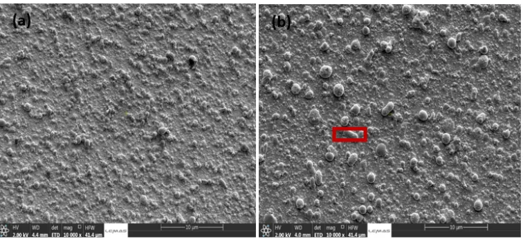
Figure 1 shows SEM images of the Er-TZN glass NPs deposited on the surface of the siloxane-coated silica substrates at the 45 µJ (sample I) and 60 µJ (sample II) energies. The purpose of these images focusses on distribution of the NPs into the polymer layer with almost identical particle sizes. It can be observed that the NPs are quite homogeneous across the entire substrate surface in Fig. 1(a). In the case of sample (II), the NPs are well separated from each other. This paper focusses on the applicability of the fs-PLD for the formation of glass-polymer composite films and reports on the basic studies on-their interface properties
[image:6.612.122.500.347.520.2]Further analysis of the SEM images with ParticleMetric software and then verified by ImageJ, the sample II reveals large number of NPs dispersed into polymer layer with irregular shape, while their size ranges from 15 to 37 nm. Their average size is estimated to be ~21 nm. On the other hand, sample I which is fabricated at the lower energy of 45 µJ shows significantly smaller particles with spherical morphology and an average particle size of ~11 nm.
Fig. 1. SEM images of the Er-TZN glass NPs deposited on siloxane polymer-coated silica substrate at (a) 45 µJ (sample I) and (b) 60 µJ (sample II).
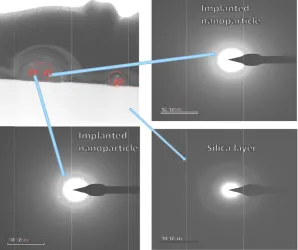
the ejected p decreases the well as crysta attributed to t [36]. The plan and 45.47 nm
Fig. 2 silica right h Fig. 3 rectan sodium polym
Figure 3 s TZN glass N
particles from number of par alline nanopart the formation n-view of TEM m for samples I
2. HRTEM image substrate modified hand side at 60 µJ
3. EDX-SEM chem ngular regions in F m (Na), zinc (Zn mer layer.
shows the cros NPs acquired f
the target to rticles and the g ticles. The nan
of α-TeO2 (pa
M measurement and II respecti
of the interface be d Er-TZN glass NP
(sample II).
mical mapping acq Fig. 1(a) and (b) n), tellurium (Te),
s-sectional ele from sample (
the substrate growth rate, w nocrystallite ob
ratellurite) and ts reveals an av ively.
etween silica matr Ps (upper left); an
quired during cross indicating the ele , oxygen (O), an
mental map of I) and sample
e (due to the which favours b
bserved in the d δ-TeO2 (tellu
verage film thi
rix and the siloxan nd SAED patterns
s-sectional STEM emental distributio nd silicon (Si) wh
f the siloxane l e (II) substrate
substrate tem build-up of fast SAED pattern urite) crystallin ickness of arou
ne polymer-coated on the bottom and
M analysis from the on of erbium (Er), hich comprises of
layer modified es. The scanni
mperature) t atoms as ns can be ne phases und 43.17 d d e , f
[image:7.612.157.455.170.420.2] [image:7.612.135.479.462.621.2]energy dispersive X-ray (EDX) spectroscopy and chemical mapping clearly show the elemental distribution of erbium, sodium, zinc, tellurium, oxygen, and silicon in the sample. The silicon, only present in the polymer is seen as thin layer over the glass particles. From both Figs. 3(a) and 3(b), it can be confirmed that the nanoparticles or clusters of glass particles are encapsulated within the polymer but without any molecular level intermixing.
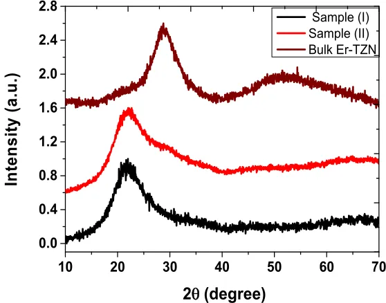
Figure 4 shows the XRD patterns obtained from the target glass and fabricated siloxane-coated silica samples modified with Er-TZN glass NPs. The target glass shows two characteristic broad amorphous bands at 2θ = 28.59° and 51.55°, while the films prepared by the fs-PLD exhibit amorphous silica evolved at 2θ = 22.5°. It is important to mention that the size of the particle generated from the target are in nano-sized, therefore, the XRD instrument could not detect the crystalline diffractions phases observed in the SAED analysis of the TEM image shown in Fig. 2. Henceforth, the presence of the crystalline phase in the polymer modified Er-TZN glass NPs could not be completely ruled out using the XRD results. For instance, Kasaai et al. [37] demonstrated the presence of crystallization in the particles irradiated from the surface of a fused silica using a femtosecond laser. However, the XRD results obtained here suggest that the irradiated surface of the fused silica remains amorphous.
10 20 30 40 50 60 70
0.0 0.4 0.8 1.2 1.6 2.0 2.4 2.8
In
te
n
sity
(
a.
u
.)
2
θ
(degree)
[image:8.612.151.430.307.526.2]Sample (I) Sample (II) Bulk Er-TZN
Fig. 4. XRD pattern obtained from the bulk Er-TZN target glass and Er-doped polymer at sample (I) and sample (II).
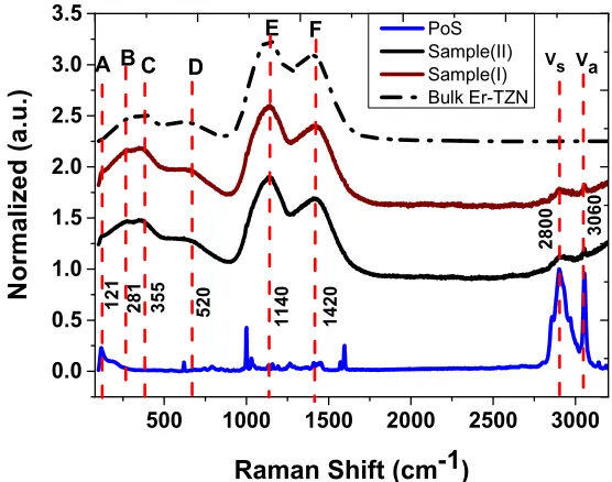
The Raman spectra of the unmodified polymer thin film and the modified layer with the Er-TZN glass NPs at the two different pulse deposition energies obtained under a 514.5 nm excitation are shown in Fig. 5. The Raman spectra reveal two bands with peaks at 2800 cm−1
and 3060 cm−1 in all the three samples, which, however, are not observed in the bulk target
glass sample. These Raman bands correspond to methyl-group (CH3) symmetric (Vs) and
asymmetric (Va) stretching vibrations [36]. Also, the Raman spectrum for the unmodified
polymer thin film exhibits additional vibration bands centred at ~616, 1126, 1418, and 1600 cm−1. These however, are not detected in the modified polymer layer with the Er-TZN NPs.
The peak occurring at 616 cm−1 can be assigned to symmetric and asymmetric stretching of
Si(–O–CH3)3 or SiC3 stretch, while the 3 remaining bands (1126, 1418, and 1600 cm−1) can
polymer thin film with Er-TZN NPs yielded additional broad bands that comprised three vibration modes in the 100-480 cm−1, 480-890 cm−1, and 890-1860 cm−1 frequency ranges.
This clearly shows a noticeable difference between the plain polymer sample (PoS) and the Er-doped polymer samples. According to Mazzuca el at [41], the sharp shoulder identified at 121 cm−1 (peak A) is attributed to vibrations due to the TeO
4–ZnO6–TeO3 chain structure. The
Zn acts as a glass network-forming link, which agrees with ZnTeO3 and Zn2Te3O8 crystals
vibrational wavenumbers. The Raman shift frequency observed at 281 cm−1 (peak B) is
assigned to TeO3 trigonal pyramids (tp) and Er–O bonds [39], whilst the peaks around 355
cm−1 (peak C) are attributed to the Zn-O content [40, 42]. The vibration band at 480-890 cm−1
which is centred at 620 cm−1 (peak D) corresponds to stretching vibration of the metastable or
B-Phase Er2O3 (B- Er2O3) groups, respectively [43]. Following Jinqiu et al. [44], higher
vibration bands centred at 1140 and 1420 cm−1 (peaks E and F) are ascribed to B-Er 2O3
bonds, respectively.
500 1000 1500 2000 2500 3000
0.0 0.5 1.0 1.5 2.0 2.5 3.0 3.5
281
F
121
3060
2800
1420
1140
520
355
E D
C
B Va
N
o
rm
al
ize
d
(
a.u
.)
Raman Shift (cm-1)
PoS Sample(II) Sample(I) Bulk Er-TZN
Vs
[image:9.612.152.430.275.494.2]A
Fig. 5. Raman spectra using 514.5 nm laser as excitation source of bulk sample, polymer coated silica, and modified with Er-TZN NPs at sample (I) and sample (II).
3.2 Optical characteristics of hybrid polymer with erbium-based nanoparticles
Figure 6 shows a comparison of the normalized photoluminescence spectra obtained from the Er-doped polymer samples at room-temperature and the bulk target sample under a 980 nm laser diode excitation. The fluorescence peak centred at 1534 nm is assigned to the transition from the first excited state (4I13/2) to the ground state (4I15/2) of the Er3+ ions. The figure
clearly exhibits a broad and intense band for the bulk glass sample with a FWHM of 51 nm. For the fabricated samples, the FWHM of the central 1534 nm peak was reduced to 39.2 nm. The fluorescence lifetime of the target and fabricated samples were measured around 1534 nm (4I
13/2 transition) using the same 980 nm excitation. The experimental data was fitted with
to fluorescence quenching induced by the C-H phonon vibration bonds in the polymer centred at 2800 cm−1 and 3060 cm−1.
1400 1450 1500 1550 1600 1650 1700 0.0
0.2 0.4 0.6 0.8 1.0
N
o
rm
aliz
e
d
in
te
n
si
ty
a
.u
.)
Wavelength (nm)
Sample (II) Sample (I) Bulk Er-TZN
[image:10.612.162.432.147.360.2](a)
Fig. 6. Normalized photoluminescence spectra of bulk Er-TZN target glass, and polymer modified with Er-TZN NPs (sample (I) and sample (II)) at room temperature via 980 nm continue wave (cw) excitation source.
400 600 800 1000 1200 1400 1600 1800 2000 40
50 60 70 80 90 100
Transmittance (%)
Wavelength (nm)
[image:11.612.159.430.110.316.2]PoS Sample (I) Sample (II)
Fig. 7. Transmittance of plain polymer-coated silica samples and samples modified with Er-TZN NPs glass processed for sample (I) and sample (II).
4. Conclusions
In this work, we present a novel technique to deposit Er-TZN glass NPs on polymer films using fs-PLD. The evaluation of the morphological, compositional and structural characteristics of the Er-TZN glass NPs deposited in the polymer layer does not indicate any significant structural modification of the NPs when compared with the properties of the target material. The SEM images and FIB-TEM measurements reveal the dependence of the size of the deposited NPs and thickness of the produced glass film on the laser pulse energy. Hybrid polymer-Er-TZN glass NPs embedded polymer films are fabricated using this method. A PL FWHM of 39 nm and an Er lifetime in the range of 3.52 to 4.18 ms are obtained under 980-nm laser excitation. Although some differences in the obtained FWHM and Er lifetime values are observed between the fabricated samples and the bulk target material, the obtained results are promising for the formation of hybrid optical waveguide amplifiers and sensing.
Funding
EPSRC (EP/M015165/1); IPES CDT (EP/L015455/1).
Acknowledgments