International Journal of Innovative Technology and Exploring Engineering (IJITEE) ISSN: 2278-3075, Volume-8 Issue-12, October 2019
Abstract: The electro-optic effect is one of the most important
techniques for modulation and switching purpose in optical communication. The Mach–Zehnder interferometer (MZI) structure functioning on the principle of electro-optic effect behaves as the influential optical switching device. This paper contains discussion of electro-optic effect based MZI structure and its efficient application to construct parity generator and checker. Titanium (Ti) in-diffused lithium niobate profile of MZI through computer simulation has been used for this purpose. Basic 2*2 switch is transformed as MZI for the design of parity device over a functional wavelength range of 1.3 µm to 1.65µm. This simulated design is analyzed with different Ti-LiNbO3 stripe thicknesses, in order to attain the optimum Ti-LiNbO3 stripe thickness and also to improve the performance of the switch on its crosstalk, power imbalance, extinction ratio and transition losses. The simulation model of proposed optical parity device has been implemented using the OptiBPM and OptiSystem softwares have
been used for suitable verification of the discussed schemes.
Keywords : Electro-optical devices, Optical logic devices,
Integrated optoelectronic circuits, Lithium niobate, Modulators.
I. INTRODUCTION
O
ne of the most vital objectives of optical digital computation techniques is to develop the performances of basic and complex digital devices. Optical logic device is a better alternative to process the information with high speed as it can realize a number of operations such as multiplexing, switching, addressing, coding/decoding and complex digital computations. Hence, it is a timely interest of many researchers to realize various logic gates optically, and XOR and XNOR in particular. Because, these two optical logic devices provide way for realization of number of other functions such as equality detectors, parity generators and code converters also. The ultrafast all-optical XOR gate using two types of semiconductor optical amplifier based SOA-MZI was analyzed and key parameters were optimized through mathematical simulations by Zhang et al.[1]. The electro-optic effect based optical switching phenomena in MZI was efficiently considered and it was broadly investigated to implement the optical full adder and full subtractor by Ajay Kumar et al.[2]. In digital communication, parity generator and checker had been used to retrieve the lost information. But, realizing them optically was not possible forRevised Manuscript Received on October 05, 2019. * Correspondence Author
Arunya Revathi A*, EEE department, Alagappa Chettiar Government College of Engineering & Technology, Karaikudi, TamilNadu, India. Email: [email protected]
Hemadevi N, EEE department, Alagappa Chettiar Government College of Engineering & Technology, Karaikudi, TamilNadu, India. Email: [email protected]
many years. Now, the optical communication era also tends to focus towards secured communication of information without any loss. This paper analyzes the ways and means of utilizing the electro-optic effect based MZI to accomplish the mission of designing such parity generator and checker optically by computer simulation. Electro optic effect is a change in refractive index of a material for a variation of intensity of applied electric field. This effect has speed less than 1ns [3]. Mach zehnder modulator plays major role in fiber optic network and it had been designed with various materials like LiNbO3 [4], semiconductors [5], and polymers [6] etc. With the help of this design, Boolean function generators [2], switches [7], logical gates [8], encoders [9], and routers [10], had been realized by computer simulation. Compared to its digital counterpart, optical parity devices provide less cross talk, efficient transmission of larger data over longer distance and wide wavelength range. In this paper, we have implemented optical parity device with the help of MZI through Beam propagation method (BPM) by computer simulation.
This paper is organized as follows. Section 2 describes the specification of the parity device and its design. Section 3 describes the simulation and implementation of the device. Section 4 describes the analyses of important factors that influence the performance of the device. Section 5 deals with the integration of optical device into an optical network using OptiSystem software. Finally, conclusion is given in section 6.
II. DESIGN
MZI switch is made on a z-cut wafer of LiNbO3 and is surrounded by air cladding. MZI switch is designed with 33 mm length of LiNbO3 wafer with 10 µm of thickness and 0.1mm of width. As-designed single bit parity device is shown in Fig.1. Introducing electrode to this MZI forms a Mach Zehnder Modulator. This Mach Zehnder Modulator is a combination of 3dB coupler (Splitter and Combiner), delay lines and electrodes.
In order to achieve optic switching, Titanium indiffusion with LiNbO3 serves the principle of perfect electro-optic behavior. The indiffusion process is done by insertion of a Ti-strip of fixed thickness and width on LiNbO3 substrate followed by heating. After this process, the titanium ions penetrate into the host substrate and form a graded index waveguide.
The above concepts of Ti-indiffusion process within LiNbO3 substrate are mainly taken from Technical Background and Tutorials, ver. 9, Optiwave Inc. 2009 [16].
Array of Mach Zehnder Modulators for
Realization of Parity Generator/Checker
The bell-shaped refractive index can be characterized by diffusion lengths or, as an alternative, by diffusion constants, diffusion temperature and a diffusion temperature coefficient for their distributions of graded waveguide in lateral and in-depth directions.
[image:2.595.313.540.193.309.2]Ti-LiNbO3 MZI provides better performances compared to other doping materials into LiNbO3 and the effective operating optimum voltage of the electrode is chosen as 6.75 V [11]. The central electrode is energized to achieve the required switching function and realize the parity bit generation. The initial device parameters such as wafer properties, electrode specification and Ti-LiNbO3 channel profile specification are tabulated in Tables 1, 2 and 3 respectively.
Fig.1. Parity Generator waveguide structure for 1 bit sequence
Table 1. Wafer Properties Substrate -
LiNbO3
Propagation direction – Y Crystal Cut – Z
Thickness - 10 µm
Electro optic coefficient - 3 to 32*e-12 m/v
Wafer Profile - LiNbO3
Length – 33 mm Width - 0.1 mm Material
air/cladding
[image:2.595.57.291.227.345.2]Thickness - 2 µm Refractive index – 1
Table 2. Electrode Specifications
Table 3. Ti: LiNbO3 Channel Profile Specification
Stripe thickness before diffusion 0.05 µm
Lateral diffusion length 4.0 µm
Diffusion length at depth 3.5 µm
The number of MZIs in the parity generator depends upon the number of bits. The MZIs are concatenated and the last Mach Zehnder modulator in this connection generates the required output parity bit. The bit sequence (Odd (or) Even) decides the generated parity bit of lower arm and upper arm of the last Mach Zehnder modulator. That is, for an even sequence, the last Mach Zehnder modulator output of lower arm is even parity generator. Likewise, for an odd sequence, the last Mach zehnder modulator lower arm output is odd
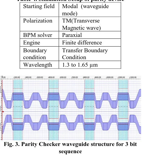
parity generator. A three bit parity generator is obtained by a cascade connection of three MZIs as shown in Fig.2 and the electrodes have been placed at the middle of the longer linear waveguides to control the output signal. In this design, right end of the lower arm is output of odd parity generator and the upper arm is output of an even parity generator. In addition to this realization of parity generator with three MZIs, we can realize the parity checker function by adding one more stage of MZI to the parity generator as shown in Fig.3. The initial simulation parameters such as, global field, polarization, engine and boundary condition are tabulated in Table 4.
[image:2.595.310.545.348.606.2]Fig. 2. Parity Generator waveguide structure for 3 bit sequence
Table 4. Simulation Setup of parity device Starting field Modal (waveguide
mode)
Polarization TM(Transverse Magnetic wave) BPM solver Paraxial Engine Finite difference Boundary
condition
Transfer Boundary Condition
Wavelength 1.3 to 1.65 µm
Fig. 3. Parity Checker waveguide structure for 3 bit sequence
III. SIMULATION
OptiBPM simulation software is used to analyze and demonstrate the proposed structure. OptiBPM essentially works on the principle of Finite Difference Beam Propagation method (FD-BPM) and provides the whole information of the optical waveguide depending upon its refractive index profile, structure,
and material used for the construction of the optical waveguide. An optical signal can be followed at any point as it propagates along a guiding
structure of designed integrated
optics. BPM allows
Applied voltage 6.75 V
Length 10 mm
[image:2.595.90.266.535.583.2]International Journal of Innovative Technology and Exploring Engineering (IJITEE) ISSN: 2278-3075, Volume-8 Issue-12, October 2019
computer-simulated scrutiny of the light field distribution where the radiation and the guided field can be examined concurrently. The MZIs based parity device is analyzed by paraxial BPM solver with finite difference engine scheme parameter of 0.5 and using transparent boundary condition method. The global data is introduced as refractive index MODAL and TM polarized test signals from wavelength 1.3 μm to 1.65 μm is analyzed.
In this design we consider the electrode voltage as the input bits and it controls the optical signal which passes through the waveguide structure to the receiving end. The control signals X, Y and Z are the voltage applied at the middle electrode of first, second and third MZIs respectively. When an optical signal is applied at the input of MZI, as per the working principle of the MZI the light output is obtained at the lower arm of the output of MZI when no electric field is applied across the electrodes. But, when an electric field is applied across the electrodes, then the Ti-LiNbO3 channel experiences a change in its refractive index in one of the arms which makes the output signal to get shifted to the upper arm. This principle is well exploited in the design of parity generator and checker in this paper.
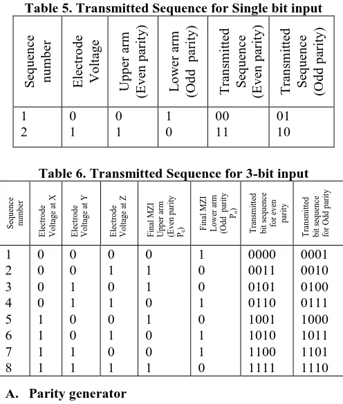
[image:3.595.306.550.120.224.2]The continuous wave optical signal is applied at the input port of MZI-1. Here, no signal is provided at the second input terminal of MZI-1 and finally output of MZI-3 is nothing but generated parity bit of given sequence. Here we use odd parity bit sequence and hence the lower arm of the last waveguide generates the odd parity and upper arm of the waveguide generates even parity. The optical field intensity distribution of Parity Generator and checker for the two different input sequences are as shown in Fig 4, 5, 6 and 7. The output transmitted sequence (along with parity bit P) for the single and three bit input sequence are tabulated in table 5 and 6 respectively.
Table 5. Transmitted Sequence for Single bit input
Seq u en ce n u m b er E lectr o d e Vo ltag e Up p er ar m (E v en p ar ity ) L o wer ar m (Od d p ar ity ) T ran sm itted Seq u en ce (E v en p ar ity ) T ran sm itted Seq u en ce (Od d p ar ity ) 1 2 0 1 0 1 1 0 00 11 01 10
Table 6. Transmitted Sequence for 3-bit input
S eque nc e number E lec tr ode Voltage a t X E lec tr ode Voltage a t Y E lec tr ode Voltage a t Z F inal M Z I Uppe r ar m (E ve n pa rit y Pe ) Final
M Z I L owe r ar m (Odd pa rit y Po ) T ra ns mi tt ed bit s eque nc e for e ve n pa rit y T ra ns mi tt ed bit s eque nc e for Odd pa rit y 1 2 3 4 5 6 7 8 0 0 0 0 1 1 1 1 0 0 1 1 0 0 1 1 0 1 0 1 0 1 0 1 0 1 1 0 1 0 0 1 1 0 0 1 0 1 1 0 0000 0011 0101 0110 1001 1010 1100 1111 0001 0010 0100 0111 1000 1011 1101 1110
A. Parity generator
When X = 0 V (logic 0), Y = 0 V (logic 0) and Z= 0 V (logic 0), where all the electrode voltages (X, Y, Z) are in the
OFF state, the optical signal applied to the input of MZI-1 generated as Odd parity at the output port 2 of the MZI-3 as shown in Fig.4. So the generated parity bit Po is 1 and Pe is 0. As shown in table 6, the selection of output port decides the transmitted bit sequence and the type of parity generator.
Fig. 4. Optical field intensity for the sequence X= 0 V, Y= 0 V and Z= 0 V
[image:3.595.308.551.305.403.2]When X = 0 V (logic 0), Y = 6.75 V (logic 1) and Z= 0 V (logic 0), the electrode voltages for X and Z are in the OFF state and the electrode voltage for Y is 6.75 V. Now the optical signal generated as even parity at output port1 of MZI-3 as shownFig.5. As shown in table 6 the generated Parity bit Po is 0 and Pe is 1.
Fig.5 Optical field intensity for the sequence X= 0 V, Y=6.75 V and Z= 0 V
B. Parity checker
[image:3.595.43.291.467.759.2]Now the transmitted sequence consists of 4 bits due to the addition of parity bit. As already stated, here another MZI is added for the Parity checker function. If the transmitted sequence is X = 6.75 V (logic 1), Y = 0 V (logic 0), Z = 0 V (logic 0) and P= 6.75 V (logic 1) (even parity transmitted signal), the electrode voltages for X and Y are in the OFF state, and the electrode voltages for Z and P are in 6.75 V, then the Checker output is enabled at even parity port of MZI-4 as shown in Fig.6.
Fig. 6 Optical field intensity for the sequence X=6.75 V, Y= 0 V, Z=0 V and P= 6.75 V
[image:3.595.303.552.526.630.2]Fig.7 Optical field intensity for the sequence X= 0 V, Y= 0 V, Z= 0 V and W=0 V
C. Analysis of Parity generator
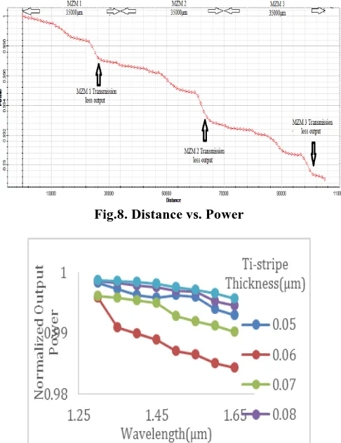
[image:4.595.48.291.392.708.2]The normalized output power of parity generator with respect to distance is plotted in Fig.8. According to this, the power and the distance are inversely proportional. i.e., If the number of input bit sequence is increased, then it will increase the number of MZIs and the respective distance of optical signal propagation. This increase in distance will limit the normalized power at the optical output. At each MZI some amount of transmission loss has occurred. As per the Fig.8, the normalized output power is 0.9886, which is 98.86% of the input power. Normalized output power with respect to different wavelengths in the range of 1.25 µm to 1.65 µm for various Ti-stripe thicknesses from 0.05 to 0.09 µm at the interval of 0.01 µm is also plotted Fig.9. From the graph, we can comprehend that by increasing the thickness and wavelength, the Normalized power is reduced. The maximum amount of power loss is 1.14% of the input Power at the wavelength of 1.65µm and at the thickness of 0.06 µm.
Fig.8. Distance vs. Power
Fig.9. Normalized output Power vs. Wavelength (µm) for various Ti stripe Thicknesses (µm)
IV. ANALYSIS OF SOME IMPORTANT FACTORS INFLUENCING THE PERFORMANCES
Optical power imbalance (PI) [12, 14] is defined as the ratio of power in cross state output waveguide, relative to the power in the bar state output waveguide. The power imbalance should be very low in order to maintain very low crosstalk in optical waveguides. The power imbalance at the output splitter of MZI can be obtained using the equation (1),
--- (1)
Where, X is maximum output power at splitter and Y is minimum output power at splitter. The extinction ratio (ER), the optical intensity at the ON state and the OFF state, is determined by the optical signal balance among the output two arms of MZI after the influence of input sequence [13]. It can be calculated using equation (2).
--- (2)
Fig. 10 depicts that the power imbalance at the end of the splitter is the worst when the wavelength increases. As in equation 2, Extinction ratio (ER) is the ratio of optical output power levels of digital signal 1 and 0. It shows that the optical power difference among the two arms to represent the parity bit depends upon the different optical losses in both the arms of MZIs as well as the power imbalance of the optical splitter. Thickness of the Ti-stripe too plays a role in it [13]. High value of ER can be obtained by modifying the Ti stripe thickness [13].
Fig.10. Power Imbalance (dB) vs. Wavelength (µm) for various Ti stripe Thicknesses (µm)
[image:4.595.303.550.446.596.2]International Journal of Innovative Technology and Exploring Engineering (IJITEE) ISSN: 2278-3075, Volume-8 Issue-12, October 2019
Fig.11. Extinction Ratio (dB) vs. Wavelength (µm) for various Ti-stripe thicknesses (µm)
Cross talk (CT) is defined as a phenomenon by which a signal transmitted on one channel of a transmission system creates an undesired effect in another channel. Here cross talk [15] at the end of the interferometer arms is as in equation 3,
--- (3)
Where,
--- (4)
--- (5)
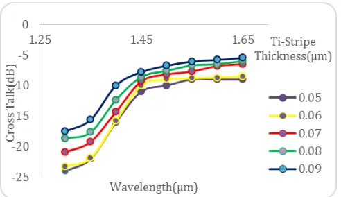
[image:5.595.301.549.50.209.2]We know that, P and Q are the power levels at the end of the MZI upper and lower arms respectively and they are given in equations 4 and 5 respectively. Here, the crosstalk measurement is carried out at the MZI1 output of our proposed device and the results are plotted in Fig.12. It depicts that the crosstalk levels at the end of the interferometer arms and it increases as the wavelength increases. The lowest crosstalk of -24 dB has been obtained at 0.05 μm Ti-Stripe thickness at 1.3 μm wavelength.
Fig.12. Cross Talk (dB) vs. Wavelength (µm) for various Ti stripe Thicknesses (µm)
Transmission loss is a metric that when light travels along a channel, its power decreases exponentially with distance. Fig.13 shows the Transmission loss versus the operational wavelength ranging from 1.3 μm to 1.65 μm. It reveals that the Transmission losses can be kept at low value by taking the value of Ti-stripe thicknessesat 0.09 μm over the wavelength range of 1.3-1.65 μm.
Fig. 13. Transmission Loss (dB) vs. Wavelength (µm) for various Ti-stripe thickness (µm)
V. SIMULATION USING OPTISYSTEM
The proposed model of Parity generator in OptiBPM simulation software is tested for its genuine operation in the optical networks using OptiSystem simulation software. The scripting data of proposed model was incorporated into the
OptiBPM component in OptiSystem. The system setup for the
[image:5.595.309.545.426.579.2]parity generator with OptiSystem is as shown in Fig.14. Here, optical gaussian pulse was given as input for the parity device in the range of 2 mW at the wavelength of 1.3μm. The given input sequence of X, Y, and Z is 0, 0, and 1 respectively. The output 1 was received at the upper arm of the parity device (Pe) and at the lower arm of the parity device (Po) it was 0.
Fig.14: Parity Device system Layout in OptiSystem
[image:5.595.47.293.505.647.2]Fig.15. The simulation result of parity device for the data (001). (A) Amount of power coupled to the upper arm for
an even parity generator (Pe = 1) and (B) Amount of
power coupled to the lower arm for an odd parity generator (Po=0)
VI. CONCLUSION
This paper has included the complete discussion of digital logic phenomena such as parity generator and checker circuit. It has presented the guideline to realize the parity device using MZIs. The performance of the proposed device has been examined in order to check the desired parameters for improving various factors such as cross talk, power imbalance, extinction ratio and transition losses. The device has exhibited the finest performance when the Ti-stripe thickness was 0.05 μm over the wavelength range from 1.3 μm to 1.65 μm. The optimum value of CT was obtained at -24 dB for Ti-stripe thickness of 0.05 μm. Parity device has also been verified with OptiSystem tool where the 99.50% of input optical power is coupled to the output arm to represent the parity bit. It has also proved that our design provides very low crosstalk. The outcome of this paper will be a stepping stone for designing digital optical components, such as optical flip-flops, optical counters and optical memories. All these devices can be helpful in the field of high speed optical communication and signal processing system
.
REFERENCES
1. M. Zhang, Y. Zhao, L. Wang, J. Wang, P. Ye, Opt. Commun. 223 (2003) 301.
2. Ajay Kumar, Santosh Kumar, Sanjeev Kumar Raghuwanshi, Implementation of full-adder and full-subtractor based on electro-optic effect in Mach–Zehnder interferometers, Optics Communications 324 (2014) 93–107.
3. Rahman M.S.A., Shaktur K.M., Mohammad R., Analytical and simulation of new electro-optic3×3 switch using a Ti:LiNbO3 waveguide medium, 2010 International Conference on Photonics (ICP),2010, pp. 1–5.
4. Wol-Yon Hwang, Min-Cheol Oh, Hyang-Mok Lee, Heuk Park, Jang-Joo Kim, Polymeric 2×2electrooptic switch consisting of asymmetric Y junctions and Mach–Zehnder interferometer, IEEE Photonics Technology Letters 9(6), 1997, pp. 761–763.
5. YAHYA E.H.M, Mach–Zehnder Interferometer, M. Tech. Thesis, Faculty of Electrical Engineering, University of Technology Malaysia, April 2007.
6. Zheng C.-T., Ma C.-S., Yan X., Zhang D.-M., Design of a spectrum-expanded polymer MZI electro-optic switch using two-phase generating couplers, Applied Physics B: Lasers and Optics,102(4), 2011, pp. 831–840.
7. MAAT D.H.P., InP-Based Integrated MZI Switches for Optical Communication, PhD Thesis, Department of Applied Physics, Delft University of Technology, Delft, The Netherlands, 9 April,2001.
8. Shaochun Cao, Liping Sun, Savoie M., 2×2 MMI–MZI GaAs–GaAlAs carrier-injection optical,switch, 2010 IEEE Photonics Society Summer Topical Meeting Series, 2010, pp. 207–208.
9. R. Kaler, R.S. Kaler, Implementation of optical encoder and multiplexer using Mach–Zehnder inferometer, Optik 122 (2011) 1399–1405. 10. S.K. Raghuwanshi, A. Kumar, S. Kumar, 1 × 4 signal router using
3Mach–Zehnder interferometers, Opt. Eng. 52 (03) (2013) 035002. 11. Ghanshyam Singh*, Vijay Janyani, R.P. Yadav, Modeling of a high
performance Mach–Zehnder interferometer all optical switch, optical applicata(2011).
12. V. Janyani Singh, R.P. Yadav, Opt. Appl. 42 (2012) 613. 13. G.L. Li, P.K.L. Yu, J. Lightwave Technol. 21 (2003) 2010.
14. Suzuki K., Yamada T., Moriwaki O., Takahashi H., Okuno M., Polarization-insensitive MZI switch composed of an LN phase shifter array and silica-based PLC-integrated polarization beam splitter,Conference on Optical Fiber communication/National Fiber Optic Engineers Conference, 2008,OFC/NFOEC 2008, pp. 1–3. 15. S. Kumar, S.K. Raghuwanshi, A. Kumar, Implementation of optical
switches by using Mach–Zehnder interferometer, Opt. Eng. 52 (9) (2013) 097106.
16. OptiBPM, Technical Background and Tutorials. Waveguide Optics Modeling Software System, Version 9.0, Second Edition, Optiwave Inc., 2009.M. R. E. Lamont, Y. Okawachi, and A. L. Gaeta, Opt. Lett.
38, 3478 (2013).
AUTHORSPROFILE
Arunya Revathi A received her B.E. degree in Electrical & Electronics Engineering from Madurai Kamaraj University, Madurai, India, in the year 1998, M.E. degree in Power System Engineering from Madurai Kamaraj University, Madurai, India,in the year 1999 and Ph.D., degree in Electrical Engineering from Anna University Chennai, India in 2009. She is currently working as an Associate Professor in the Department of EEE, Alagappa Chettiar Government College of Engineering & Technology, Karaikudi, India. She has published papers in International & National journals & Conferences. Her current research interests include power system, Power Electronics, Digital Electronics, Photonic Crystals and Metamaterial. She has 20 years of teaching as well as research experience in various fields.