Abstract: Electrostatic discharge (ESD) can extremely damage and affect the operation of the electronic devices which is mainly due to the discharge of static electricity through the human or an object contact to the electronic devices. Though ESD protection has been made in many ICs internally, it can only sustain a certain level of voltage surge. To withstand high voltage surge mainly above 4kV, external ESD protection devices such as ESD capacitor and TVS (Transient Voltage Suppressor) are used for signal integrity considerations. For automotive application using 12V battery, a circuit model which has the capability to explain the behaviour of the ESD protection device for 8kV is proposed. Comparison between simulation by LTspiceXVII and calculated results are shown and also presents the pros and cons of two different approaches. When comparing ESD capacitor to TVS diode, the result shows 32.8 percentage reduce in voltage, 1 percentage increase in current and 1.43 percentage reduce in power dissipation. In addition to the theoretically calculated capacitor value, other capacitors are used and its results were presented
Keywords : About four key words or phrases in alphabetical order, separated by commas.
I. INTRODUCTION
[image:1.595.323.490.209.373.2]Static electricity is discharged when two electrically charged objects come into contact with each other as shown in Fig. 1. The charged bodies in contact could be any electronic device with a human body. This occurrence is called ESD (Electrostatic Discharge). A human body can generate ESD of the order of several thousand volts. The IC circuit present inside the electronic device will tend to be damaged or might breakdown when this high voltage pulse enters. Hence it is necessary to use the components that suppresses or removes ESD so that the destruction of a product or system when touched can be eliminated. The harmful effects of ESD on sensitive assemblies and electronic devices are documented and receive significant attention, in handling and design procedures. Due to this factor, there is a strict packaging, handling and design requirements on suppliers by the Department of Defense and many other companies. The harmful effects that ESD has on sensitive electronic devices and assemblies are well documented and receive significant attention, both in design and in handling procedures. The
Revised Manuscript Received on November 06, 2019.
G.V.Ashwini, ECE Department, SNS College of Technology, Coimbatore, India . Email: [email protected]
Dr.S.Chenthur Pandian, ECE Department, SNS College of Technology, Coimbatore, India . Email: [email protected]
D.Ruth Anita Shirley, ECE Department, Sri Krishna College of Engineering and Technology, Coimbatore, India. Email: [email protected]
[image:1.595.336.529.480.655.2]Department of Defense and many companies place strict design, handling, and packaging requirements on suppliers.
Fig. 1.Example of ESD Sources
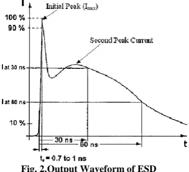
Conversely, till date, insufficient emphasis has been placed on correctly managing a comprehensive program to alleviate the effects of ESD and the success of ESD depends on its handling techniques. Fig. 2 shows the output waveform of ESD generator which is the standard (ISO 10605) waveform for describing a typical ESD event at the system level and is differentiated by its sub nanosecond rise time and high current level.
Fig. 2.Output Waveform of ESD
The ISO 10605 standard specifies four levels of ESD voltages and most of the products should pass the highest levels i.e. 8kV contact discharge or 15kV air discharge. As discussed earlier, ESD results in the high voltage spark which is indicated as initial peak (Imax) followed by second peak current as shown in Fig. 2. It is the duty of the designer to resist this peak current in entering the sensitive semiconductor device.
Mitigating the Effects of ESD using ESD
Capacitor and TVS Diode
Table- I: ESD level rating
Level
Test voltage (Contact discharge)
(kV)
First peak current (Amp)
Test voltage
(Air discharge)
(kV)
Peak current
at 60 ns (Amp)
Peak current
at 30 ns (Amp)
1 2 7.5 2 2 4
2 4 15 4 4 8
3 6 22.5 8 6 12
4 8 30 15 8 16
II. PROCEDUREFORPAPERSUBMISSION
A. Necessity for ESD protection
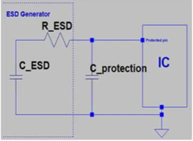
[image:2.595.76.268.320.460.2]ESD countermeasures are essential where electrical devices are likely to come into contact with an object or a person. An example include LAN, USB output terminals or any points where user connects or disconnects a connector, such as boards are connected to each other using a connector or an operation button of an electrical product is touched. ESD might also reflect when a person or a device touches a board during the production process.
Fig. 3.Decreased ESD sensitivity with a protection capacitor
B. ESD Test Method
Good ESD protection circuitry is included in all the semiconductor devices. As per JEDEC standards, in order to certify their efficiency and dependability requirements, ESD tests are required to meet the requirement parts. ESD tests has three main models: the machine model (MM), the charge device model (CDM), and the human body model (HBM). Out of these tests, HBM is considered as the most commonly used test method for ESD resistance of capacitors. ESD is simulated in HBM based on the assumption than static charge is discharged from human beings. Human beings are considered a prime source of ESD. In CDM the simulation is based on the assumption that static is discharged from a machine. MM represents a discharge from an electrified device. The thing could be any tool or production equipment.
III. ESDCAPACITORVALUECALCULATION
ESD capacitor is the very common method of protecting sensitive circuits by placing the capacitor between the exposed pin and ground. By doing so, the capacitor can bypass the ESD current to the ground and protect the sensitive device. From fig.3, we can see that between ESD generator
and the external (protection) capacitor, a capacitive voltage divider is formed. Here, R_ESD and C_ESD are the resistance and capacitance of the ESD generator. For HBM, charge is equal to capacitance times voltage (Q= CV) and the total charge is transferred from ESD generator to the external protection capacitor it follows that,
Where
CESD - ESD capacitance of the generator VESD - ESD voltage of the generator
Cprotection - ESD protection capacitor value
Vprotection - ESD protection voltage value
Knowing the ESD capacitance and voltage of the generator as well as the maximum voltage that can be allowed at the IC, the value of the protection capacitor can be calculated from the equation given below.
Where
Cgun - Capacitor value of the gun (150pF)
Vbr-ESD - ESD breakdown voltage which is considered
as 45V for automotive applications Vgun - Voltage of the gun
From equation 2, the value of Cprotection can be calculated and be used as an external capacitor to resist ESD entering into the IC.
TABLE- II: CPROTECTION VALUE
Vgun (kV)
C protection (nF)
Available C protection Value
(F)
2 6.6 6800p
4 13.2 0.013µ
6 20 0.02 µ
8 26.6 0.027µ
The Cprotection value has been calculated for different range of Vgun values in reference with Table 1 and is tabulated in Table2. The calculated Cprotection value may not be available in the market, so the available capacitor value equivalent to
Cprotection has been tabulated in Table 2.
IV. TVSDIODES
TVS diodes are semiconductor devices which act as fast response clamping diodes. TVS diodes are not normal PN diodes which are also used for clamping. TVS is similar to the operation of Zener diode. The operation of the device is such that, the device clamps when it reaches breakdown. Otherwise, it is an open circuit.
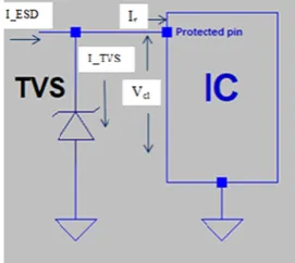
Fig.4 shows the TVS symbols. In the figure, A and B are bidirectional TVS whereas C is a unidirectional diode. ESD may be positive or negative pulse. Bidirectional TVS diode can able to block both positive and negative sharp rising ESD pulse. On the other hand, a unidirectional TVS can only suppress one directional spike. Fig. 5 shows the ESD protection system where TVS diode is used to protect the IC.
*
*
ESD ESD protection protection
C
V
C
V
*
gunprotection gun
br ESD
C
C
V
V
When ESD arrives at the protection line, the TVS diode conducts and clamps the voltage to its clamping voltage (Vcl) averts maximum of the current (I_ESD) to ground. Though, some amount of current still flows into the protected line which is called as residual current (Ir).
Fig. 4.TVS diode symbol with different types available
[image:3.595.324.540.245.371.2]Since TVS diodes respond to the ESD spikes quickly, it is widely used in automotive applications. While selecting TVS diodes, the following parameters such as, breakdown voltage (VBR), peak pulse current (Ipp), ESD rating, transient surge clamping voltage (Vcl) and the dynamic resistance (Rd) should be found.
Fig. 5.TVS diode protection circuit for arresting ESD effects
The clamping voltage (Vcl) is calculated by the breakdown voltage (VBR), peak pulse current (Ipp) and the dynamic resistance (Rd). Equation 3 gives the relationship between above said parameters such as
*
BR pp d
Vcl
V
I
R
(3) Where
Vcl - Clamping voltage
VBR - Reverse breakdown voltage Ipp - Peak pulse current
Rd - Dynamic resistance
The value of Vcl has high impact on the product of Ipp and Rd than VBR due to the high amplitudes associated with ESD currents. Depending upon the clamping voltage, the appropriate TVS diode can be selected for the particular application. TVS diode used in the simulation is SLD8S26A which is manufactured by Littlefuse.
According to the automotive standards, for selection of components (TVS) some parameters should be kept in mind which are clamping voltage, peak power dissipation and surge current.
The IC used for automotive application can‟t sustain if the input voltage is given more than 45V, for this reason 42.1V clamping voltage is selected. The component SLD8S26A is selected because it meets the requirement satisfying automotive standards and its parameters are:
clamping voltage is 42.1V, peak power dissipation of 500W and surge current of 100A.
V. RESULTSANDDISCUSSION
A. Simulation Results
[image:3.595.110.246.313.434.2]The ESD model has been simulated and the simulation is done using LTspiceXVII. The ESD input voltage of 8kV (Fig. 2)is applied to the capacitor and TVS diode separately. By applying the input voltage and its corresponding output voltage (at the capacitor and TVS diode), current (at the capacitor and TVS diode) and average power dissipated (for 30ns time interval) by the capacitor and TVS diode is analysed. Since the circuit is used for automotive applications, 12V battery is connected with ESD generator which indicates ESD is applied to the powered line.
Fig. 6.Simulation model of ESD generator
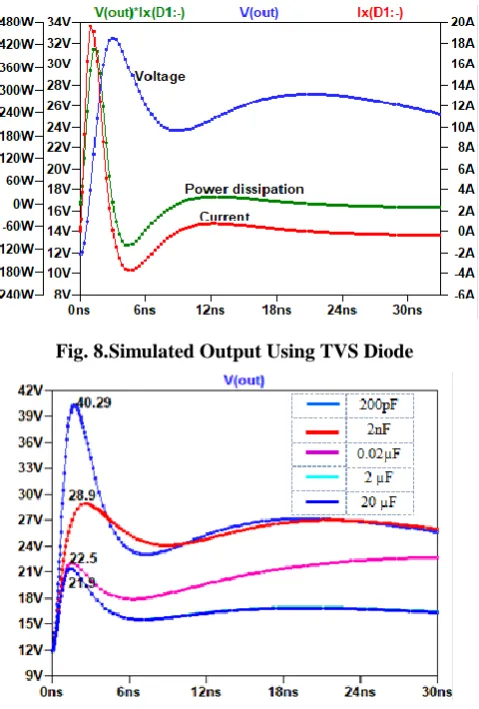
The simulation model of ESD generator is shown above in fig.6. Initially the ESD pulse is applied to a capacitor of 0.027µF as calculated from table 2. The output voltage, current and power dissipated by the capacitor was analysed.From the fig.7, it is evident that, the peak voltage, current and average power dissipated by capacitor due to 8kV ESD pulse was 22.5V, 19.5A and 127.3W (for 30 ns interval).Secondly, the ESD pulse is applied to a TVS diode and the above said parameters were analysed. From the fig. 8, the peak voltage, current and average power dissipated by TVS diode due to 8kV ESD pulse was 32.7V, 19.8A and 181.2W (for 4 ns interval).
[image:3.595.307.550.534.708.2]Fig. 8.Simulated Output Using TVS Diode
Fig. 9.Output Voltage Achieved Using Different Capacitors
[image:4.595.320.547.51.233.2]Finally the simulation is carried by selecting different capacitor values randomly (such as 200pF, 2nF, 0.02µF, 2µF and 20µF) in addition to the theoretically calculated capacitor value and its result was analyzed. From the result, it is seen that, selecting 0.02µF (Theoretical value) capacitor gives the optimal voltage, current and power dissipation when compared to other capacitor values. If capacitor is selected less than 0.02 µF then its ESD suppression capability is less and if selecting greater than 0.02 µF then the result remains almost constant.
Fig. 10.Output Current Achieved Using Different capacitors
Fig. 11.Power Dissipation Achieved
By using greater capacitor value has disadvantages like limiting the data speed. Hence it is better to go with the theoretically calculated capacitor value. Fig. 9, 10 and 11 shows the voltage, current and power dissipation of the capacitor used.
Table- III: Output of different capacitor selection
Capacitor (F)
Voltage (V)
Current (A)
Average power dissipation
(W)
200p 40.3 5.07 1.779
2n 29.04 15.6 15.17
0.02µ 22.5 19.5 127.3
2 µ 20.3 20.08 178.8
20 µ 20.3 20.08 178.6
From table III, using capacitor value low i.e., 200pF and 2nF, the average power dissipation (for 30ns time interval) and current is less but still the voltage is high when compared to other values. By selecting high capacitor value i.e., 2 µF and 20 µF, voltage is less when compared to 0.02 µ but current and average power dissipation becomes higher. Hence, it is better to go with the theoretical value calculated i.e., 0.02 µF for better results.
B. Comparison- ESD Capacitor and TVS Diode
The ESD electric charge is charged by the ESD capacitor by its capacitive components. Thus, when the capacitance is larger it provides high ESD suppression ability. Nevertheless, the accumulated charges are discharged after a few nanoseconds resulting in the generation of large voltage peak. This large voltage peak is a big disadvantage as it can destroy the component. The biggest advantage is its cost when compared to others. When such circuits are used in automotive applications for ESD protection the cost is less when compared to others.
A TVS diode is a protection device used for ESD suppression. The diode shows excellent ESD arresting properties when compared to the capacitor having higher capacitance. TVS diodes are very much useful in high- speed circuits where high capacitance cannot be used.
Hence, in high speed signal circuits TVS diodes are highly considered with the following properties such as uni/bi directional diode, high ESD voltage rating, low dynamic resistance and low clamping
[image:4.595.63.275.572.728.2]But the main drawback is the cost. When manufacturing in bulk, this leads to an increase in the component cost. On the other hand, ESD capacitors arebest suited for applications with signal lines speed less than 1Mbps.
VI. CONCLUSION
This paper has analysed a study of two ESD protection techniques which uses ESD capacitor and TVS diodes. The pros and cons of these two techniques were discussed. Selection of the capacitor value for different ESD voltages were calculated and tabulated. TVS diode was selected depending on the automotive application. The work conveys intriguing results that can help system designers select the apt ESD suppressor for different types of applications.
Among the two techniques studied, it has been identified that the ESD capacitor provides the most effective protection. With respect to their lower cost, ESD capacitors are often preferred to diodes in low speed signal applications. But, when it comes down to protection in high-speed lines, ESD capacitors fall short and TVS diodes are the right choice.
REFERENCES
1. T. Yoshida, "A Study on Transmission Line Modeling Method for s system-level ESD Stress Simulation", Proc. APEMC2015 SS13–1.2,
2015.
2. N. Kimura, T. Yoshida, "A Study on Response Characteristics Modeling
Method for ESD Protection Device by Vector Network Analyzer", Proc. of APEMC2017 WE-PM-4-2, 2017.
3. Takahiro Yoshida, Manabu Endo, “A study on ESD protection characteristics difference measurement of TVS diodes by VNA”, IEEE Symposium on Electromagnetic Compatibility, Beijing, China, 2017. 4. M. Honda, "A Review of EMI Problem Caused by ESD Phenomena",
13th RCJ Reliability Symposium, pp. 183-186, 2003.
5. J.R.Barnes, “Designing Electronic Systems for ESD”, Conformity Magazine, Vol. 8, pp. 18-27, Feb. 2003.H. Poor, An Introduction to
Signal Detection and Estimation. New York: Springer-Verlag, 1985, ch. 4.
6. Ram Chundru, “An Evaluation of TVS Devices for ESD Protection”, IEEE International Symposium on Electromagnetic Compatibility, Long Beach, CA, USA, pp. 62-67, 2011.
7. Che Hao Chuang, “System-Level ESD Protection for Automotive Electronics by Co-Design of TVS and CAN Transceiver Chips”, IEEE Transactions on Device and Materials Reliability,Volume: 17, Issue: 3,Sept. 2017.
8. IEC/TS 62228 ed1.0 “Integrated circuits - EMC evaluation of CANtransceivers”, 2007.
9. T. Maloney and N. Khurana, "Transmission line pulsing techniques forcircuit modelling of ESD Phenomena", EOS/ESD ymposiumProceedings (1985), pp. 49.
10. Kleveland.B., Maloney. TJ, Morgan.I.; Madden. L, Lee. T.H, Wong,S.S., "Distributed ESD protection for high-speed integrated circuits,"Electron Device Letters, IEEE, vol.21, no.8, pp.390-392, Aug. 2000.
11. „TVSDevicesandPrinciples‟,http://www.littelfuse.com/data/en/Applica tion_Notes/an9768.pdf
12. Ruth Anita Shirley.D and Dr..Sasipriya.S, “Electromagnetic interference and its effect on the printed circuit board”, in Jour of Adv Research in Dynamical & Control Systems, Vol. 10, 12-Special Issue, 2018.
13. IEC 61000-4-5 Ed.2.0, Electromagnetic Compatibility(EMC)– Part4-5:Testing and Measurement Techniques –SurgeImmunity Test, 2005.
14. IEC 61000-4-2 Ed.2.0, Electromagnetic Compatibility(EMC)– Part4-2:Testing and Measurement Techniques –ESD Immunity Test, 2008.
15. „System – level ESD protection guide‟, http://www.ti.com/lit/sg/sszb130c/sszb130c.pdf
AUTHORSPROFILE
G.V.Aswini, working as an Assistant Professor in Electronics andCommunication Department, SNS College of Technology, Anna University, Coimbatore, India, completed B.E degree in Electronics and Communication Engineering from Thiruvalluvar College of Engineering and Technology, and ME degree in Communication Systems from Crescent Engineering College, Chennai. Presently she is working as an Assistant Professor in SNS College of Technology, Coimbatore, India. Her areas of interest include signal integrity, electromagnetic compatibility, and antenna design.
S. Chenthur Pandian, working as a Principal in SNS College of Technology, Coimbatore, India, completed AMIE-„A‟: Electrical Engineering from Institution of Engineers (India), Calcutta,, AMIE-„B‟: Electrical Engineering from Institution of Engineers (India), Calcutta, Master of Engineering in Power Systems from Punjab University, Chandigarh and awarded Doctorate in Power Systems specialization from Periyar University, Salem, India. His areas of interest include power systems, fuzzy logic, Renewable Energy Sources and Neural Network.