International Journal of Innovative Technology and Exploring Engineering (IJITEE) ISSN: 2278-3075, Volume-8 Issue-9, July 2019
Abstract:In the current paper, common source Low Noise Amplifier using inductively degenerated technique is designed to meet Radio Frequency (RF) range 2.45 GHz-2.85 GHz. The designed LNA is implemented using single and multi-finger transistor logic. The transistor geometry greater than 300 μm has been split into multiple fingers using multi-finger technology. The schematic is captured using ADS. The performance of LNA for various technologies has been analyzed using PTM 180 nm, PTM 130 nm and PTM 90 nm models. The amplifier with single transistor achieves minimum noise figure of 0.178 dB noise figure and maximum gain of 20.045 dB using 130 nm model technology for Bluetooth applications. Similarly 0.288 dB of minimum noise figure and peak gain of 17.971 dB are obtained using multi-finger MOSFET of PTM 90 nm technologyrespectively.The reverse isolation (S12) below -50 dB is achieved.
Index Terms: Advanced Design System (ADS), Bluetooth, CMOS, Low Noise Amplifier, Multi-finger, RF frequency.
I. INTRODUCTION
During last two decades, wireless telecommunication systems have great development both in hardware and software aspects. Systems for wireless data communications are becoming smaller and less power consumption to minimizing the number of external components required. These transceivers have to include multi-standard concepts to create new to meet design challenges like high performance, low power consumption and low cost. The development of CMOS technology supported for the development of wireless RF transceivers. The Low-Noise Amplifier (LNA) is the most essential component in the receiving path of RF receiver. In recent RFLNA architectures, the multi-standard has been reported in many works and various implementations.The LNA is responsible for strengthening of poor received signals while minimizing the noise and non-linear distortions at output end of amplifier. The characteristics of LNA set the overall performance of RF transceiver systems [1-2]. Design of LNA for a given requirement need to meet all the parameters such as noise figure, gain, linearity, impedance matching, power
Revised Manuscript Received on July 05, 2019.
Kusuma M S, Research Scholar, Bangalore Institute of Technology, Bengaluru,India.
Dr. S Shanthala, Prof. & HOD, Bangalore Institute of Technology, Bengaluru, India.
Dr. Cyril Prasanna Raj P, Senior Member, IEEE, M. S Engineering College, Bengaluru, India
.
consumption and chip area. With the use of lumped components, in LNA design which are frequency dependent, the reactance of the LNA circuit changes with frequency [3]. LNA will increase the power of both the signal and the noise present at its input, the optimum design of LNA need to minimize the additional noise. LNA design and its behavior is characterized by five parameters such as Noise Figure (NF), gain, bandwidth, linearity and dynamic range. Designing an LNA that can meet all these parameters requiresan understanding of the active device, impedance matching, and details of fabrication and assembly to create an amplifier that achieves optimal performance with the fewest trade-offs. There are several LNA topologies such as distributed amplifier topology, Common Gate (CG), Common Source (CS), cascade and Current Reuse (CR) topology [4]. The most frequently used topology for LNA design is the common source amplifier with inductive source degeneration.
The basic Inductively Degenerated Common Source (IDCS) LNA has typically been the best choice for narrowband applications due to its low NF, high gain and low power consumption with good performance [2]. The input matching circuit consisting of the source inductors and the gate to source capacitance resonates at a single frequency [5]. The Bluetooth systems need to operate on low power signals in ISM (Industrial, Scientific and Medical) band. Therefore LNA that can minimize interference noise is required for the Bluetooth system. Interference is one of the major challenges addressed in ISM band [6-8].
II. THEORETICAL BACKGROUND
The LNA must provide good noise figure along with enough gain to overcome the noise in the successive stages of RF receiver. The design of critical component in LNA is the design of input impedance matching (50 Ω) circuit which provides source impedance for minimum noise figure (NFmin)
which leads to poor gain. There are many techniques for 50 Ω input impedance matching in which inductive source degeneration circuit exhibited NFmin [9]. The distributed
amplifier reported by Ren-Chieh Liu et al., in [10], employs multiple narrowband LNAs to realize wideband matching. The distributed amplifiers guarantees good matching performance and high power gain over wide bandwidth 0.6 GHz to 22 GHz. However, it consumes large power and results in high noise figure up to 6 dB due to multiple amplifiers. So there is still chance for existing CMOS LNAs.
Performance Analysis of Inductive Source
Degeneration Low Noise Amplifier using
Multi-finger Technique
James Wilson and Mohammed Ismail in [11] presented an inductive source degenerated LNA with independently tuning center frequency and quality of input matching network. Such that the circuit provides the fast calibration and low power consumption. This IDCS technique approaches the input match to the desired center frequency in the presence of process shifts and parasitic elements. But the same calibration loop is used to tune the desired center frequency of load tank. The authors Kuo-Liang Yeh and Jyh-ChyurnGuo have described new approach for layout dependent parasitic capacitance and mobility extraction in [12] using multi-finger technique. The optimization method is used in measuring the S-parameters associated with the intrinsic channel andeffective mobility in multifinger MOSFETs with narrow widths down to 0.125 μm. An LNA with two stage CS-CG configuration and forward body bias technology was developed by Gh.R.Karimiin [13] with NF of 2.202 dB at 2 GHz frequency of operation while consuming 0.96 mW dc power.
The design of the LNA in this work was concentrated at an operating frequency of 2.45 GHz to 2.85 GHz for Bluetooth applications. The design and simulation results of LNA using IDCS topology is developed using a Berkeley Short-channel Insulated gate field effect transistor Model 3 (BSIM). Designing a LNA for Bluetooth applications and its implementation in Advanced Design System (ADS) tool are presented in Section 3 and in Section 4. Simulation results and Results discussion are reported in section 5 and section 6 provides the conclusion.
III. LNA DESIGN METHODOLOGY
The LNA with IDCS technique is shown in Fig. 1 and the corresponding specifications of the design is given in Table 1. The 50 Ohm resistor Rs is connected across the input
terminal of LNA and hence provides the input matching. The bandwidth of the amplifier is determined by the input capacitance, Cgs of the transistor M1. The inductance Lg at the
gate of NMOS compensates the gate to source capacitance of M1 at the resonant frequency and hence making the
impedance at the input of NMOS to be real i.e., only input resistance Rin [14].
Vdd
RS Lg
Ls Lbias
Vbias
[image:2.595.327.524.218.312.2]M1
Fig. 1: Detailed circuit of CS LNA
Table 1: Narrow band LNA specifications
Parameters Specifications
Frequency (GHz) 2.45 - 2.85
Noise Figure (dB) < 2.5
Gain (dB) >10
Source/Load Impedance (Ohms)
50
[image:2.595.343.506.520.645.2]A step by step algorithmic design methodology is developed for a an IDCS LNA by considering PTM 180 nm, PTM 130 nm and PTM 90 nm models. The detailed design of LNA based on fundamental equations is presented in [15]. The circuit parameters of the proposed LNA are summarized in Table 2. The various process-dependent parameters for three different technologies such as 90 nm, 130 nm and 180 nm nodes were derived from the PTM model files [16].
Table 2:Circuit parameters for LNA design
Parameters PTM 180 PTM 130 PTM 90 Cox (pF/µm2) 8.6320E-3 10.463E-3 13.8122E-3
Lg (nH) 7.52 7.52 7.52
LS (nH) 0.5 0.5 0.5
W (μm) 434 496 489
gm (A/V) 0.045 0.045 0.045
Veff (V) 0.0618 0.0841 0.037
ID (mA) 1.39 1.894 0.832
IV. EXPERIMENTAL SETUP AND VALIDATION
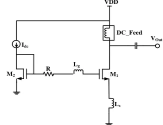
[image:2.595.83.253.545.735.2]The LNA design with circuit parameters summarized in Table 2 is modeled and simulated in ADS shown in Fig. 2. The current mirror based current reference circuit is designed to achieve constant load current flow for LNA circuit. The current mirror circuit is used to avoid extra voltage source in the circuit. The width of MOSFET M2 is times width of
M1, with M1 width set to 10M2, the power overhead of the
bias current is reduced.
A resistance R is selected so that its equivalent noise current can be ignored. This bias resistor isolates the current mirror from RF input. The capacitors connected between RF input and gate of M1 and that between drain and output
terminal of M1 are used as DC blocking capacitors. The
inductor between drain and supply isolates RF signal flowing into supply rail. The DC_feed inductor is adjusted to obtain optimum gain.
Lg
Ls
M2
VOut
VDD
Idc
M1
R
DC_Feed
Fig. 2:ADS Simulation setup to analyze the basic LNA design
Implementation
International Journal of Innovative Technology and Exploring Engineering (IJITEE) ISSN: 2278-3075, Volume-8 Issue-9, July 2019
This methodof implementation involves realizing a single transistor with larger width using multiple smaller width transistor connected in parallel. By having smaller transistor geometry, transistor matching is achieved meeting PVT corners and minimizing passive capacitance during layout design. This implementation is as shown in the Fig. 3. Multi-finger layout technique is extensively used in submicron CMOS circuit design due to increased circuit performance when compared to a single finger layout.In short channel MOSFETs, the gate resistance generates gate current noise which is significant to the thermal noise of the gate [17]. To overcome this, two methods are used to minimize the thermal noise. First method is silicide gate material which helps to reduce gate resistance (Rg) and second is multi-finger
technique where several devices (fingers) are connected parallel. Multi-finger technique allows lower gate resistance, less noise and improves the frequency performance [18]. The gate resistance is given in equation (1).
(1)
Rsh is the sheet resistance of the gate material, nf is the
number of fingers and the factor of 12 is due to the distributed nature of the gate resistance when it is contacted on both ends [9][19]. However, keep reducing the transistor finger width WF or increasing number of fingers NF can result in larger
[image:3.595.330.513.222.344.2]gate capacitance [20]. Increase in signal quality and reduce in signal reflection is achieved with good impedance matching network. The multi-finger effect on single transistor is analyzed in this work.
Fig. 3:Standard structure of multifingerMOSFET, WTot= WF X NF [12]
The sample sets used for multi-finger circuit are summarized in the Table 3. There are three samples (S1, S2, and S3) to observe the variations of gate width.
Table 3: Summary of geometric information for test circuit
S1 =200 S2 =300 S3 = 450
WF (µm) 66.66 100 150
NF 3 3 3
[image:3.595.96.238.403.494.2]The LNA design with circuit parameters summarized in Table 2 and sample sets used for multi-finger circuit in Table 3 is modeled and simulation environment is set in ADS software. The amplifying transistor M1 of Fig. 2 is divided
into three fingers M3, M4 and M5 of equal finger width and
their terminals are connected together as in Fig. 4.A detailed discussion on LNA results using single transistor and multi-finger technique is presented in next section.
V. GAIN AND NF SIMULATION RESULTS DISCUSSION
The optimized design of LNA in terms of maximizing gain and minimizing NF is considered in this section. Plots of gain and NF with the typical frequency and transistor width with different PTM models are captured with all the
process corners for single transistor shown in Fig. 5 to Fig. 14 and multiple-finger technique shown in Fig. 15 and Fig. 16.
A. Gain and NF Effects on Single Transistor Design The ADS simulations of IDCS LNA of frequency versus width and NF versus width under different PTM technology with power gain greater than 14 dB are shown in Fig. 5 and Fig. 6 respectively. The transistor with narrow width has higher frequency of operation and lower noise figure values are achieved. Similar readings are obtained for power gain less than 14 dB, shown in Fig. 7 and Fig. 8 where lower noise figure values are reported for smaller transistor width with three different PTM models.
VDD
R M2
Idc
M3 M4 M5 DC_feed
Vout
Lg
Ls
[image:3.595.330.521.460.574.2] [image:3.595.85.248.571.615.2]Fig. 4: Simulation setup to analyze themulti-finger LNA design The simulation results of Fig. 5 to Fig. 8 indicate that there is an increase in noise figure of 11.78% for 180 nm model, 15.51% for 130 nm model and for 90 nm model technology 21.03% improvement in the noise figure with 85.11% of transistor geometry. The simulation results indicate that there is a frequency improvement of 79.51% for 180 nm model, 81.92% for 130 nm model and 69.66% for 90 nm model technology with 85.11% of transistor geometry.
Fig. 5: Frequency versus width plot underdifferent technologies (gain>14dB)
Fig. 6:Noise Figure versus width plot under different technologies (gain>14dB)
0 1 2 3 4
450 300 225 200 150 100
Fr
eq
u
en
cy
(
GH
z)
width (μm)
180 130 90
0 0.2 0.4 0.6 0.8 1 1.2
450 300 225 200 150 100
N
o
ise
Fi
g
u
re
(
d
B
)
Width (μm)
180
130
[image:3.595.325.527.610.717.2]Fig. 7:Frequency versus width plot under different technologies (gain<14dB)
[image:4.595.329.531.70.223.2]Fig. 8: Noise Figure versus width plot under different technologies (gain<14dB)
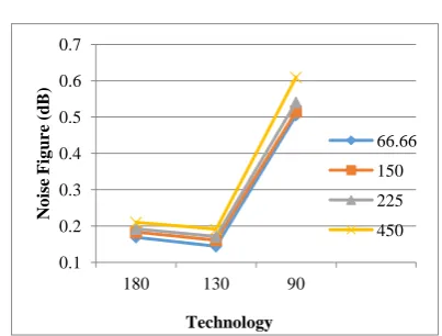
Fig. 9 and Fig. 11 are the plots of minimum noise figure of 0.169 dB for 66.66 μm transistor width with operating frequency of 5.15 GHz using 180 nm model and Fig. 10 indicates gain of 12.056 dB. The 130 nm model simulation results indicate 0.144 dB minimum noise figure at 5.45 GHz frequency of operation and gain of 12.439 dB with 66.66 μm transistor width. Similarly for 90 nm technology 0.505 dB of NFminis obtained at 5.75 GHz frequency and gain of 11.179
[image:4.595.332.520.421.539.2]dB for transistor geometry of 66.66 μm width.
Fig. 9: Frequency versus technology plot under different widths W (μm), minimum NF
Fig. 10: Gain versus technology plot underDifferent widths W (μm), minimum NF
Fig. 11: Noise Figure versus technology plot underdifferent widths, W (μm), minimum NF
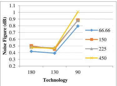
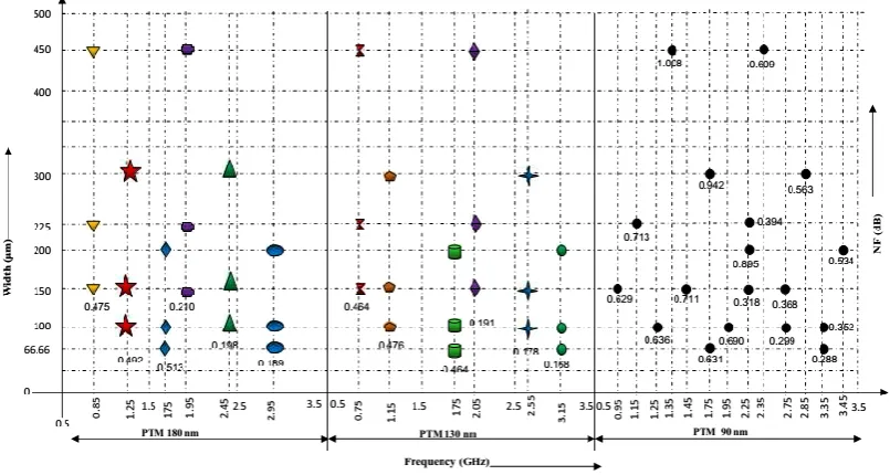
Fig. 12 and Fig. 13 indicate the maximum gain of 18.746 dB for 450 μm width with operating frequency of 0.85 GHz using 180 nm technology and Fig. 14 shows NF of 0.475 dB. The 130 nm model simulation results indicate 20.045 dB maximum gain at 0.75 GHz operating frequency and noise figure of 0.464 dB with 450 μm transistor geometry. Similarly the maximum gain of 14.646 dB is obtained with operating frequency 1.35 GHz using 90 nm technology and NF of 1.008 dB. Therefore the LNA to operate at minimum noise figure the recommended technology is 130 nm and transistor width of 66.66 μm. Similarly the LNA to operate at maximum gain the 130 nm technology is preferred with transistor geometry of 450 μm width.
Fig. 12: Frequency versus technology under different widths, W (μm), minimum NF
Fig. 13: Gain versus technology plot under different widths, W (μm)
1 1.5 2 2.5 3 3.5 4 4.5 5
450 300 225 200 150 100
Fr eq u en cy ( GH z) Width (μm) 180 130 90 0 0.2 0.4 0.6 0.8
450 300 225 200 150 100
N o ise Fi g u re ( d B ) Width (μm)
180 130 90
0 1 2 3 4 5 6 7
180 130 90
Fr eq u en cy ( GH z) Technology 66.66 150 225 450 10 10.5 11 11.5 12 12.5 13 13.5 14 14.5
180 130 90
G a in ( d B) Technology 66.66 150 225 450 0.1 0.2 0.3 0.4 0.5 0.6 0.7
180 130 90
N o ise Fi g u re ( d B ) Technology 66.66 150 225 450 0 1 2 3 4 5
180 130 90
Fr eq u en cy ( GH z) Technology 66.66 150 225 450 12 13 14 15 16 17 18 19 20 21
180 130 90
[image:4.595.74.262.474.586.2] [image:4.595.327.524.576.725.2] [image:4.595.75.264.642.770.2]International Journal of Innovative Technology and Exploring Engineering (IJITEE) ISSN: 2278-3075, Volume-8 Issue-9, July 2019
Fig. 14: Noise Figure versus technology plot underdifferent widths, W
(μm)
The LNA circuit to operate for Bluetooth applications, the required NFmin of 0.192 dB and gain of 13.166 dB using 180
nm technology are obtained with a transistor width of 225 μm. TheNFmin of 0.178 dB and power gain of 13.941 dB
using 130 nm model technology are obtained with 300 μm transistor geometry.Similarly the NFmin of 0.563 dB and gain
of 11.132 dB are obtained using 90 nm model technology with a transistor geometry of 300 μm width. The maximum gain of 14.646 dB is obtained for 150 μm width and noise figure of 0.884 dB using 90 nm technology for Bluetooth applications of LNA circuit.
B. Power Report for Single Transistor Technique The 90 nm length design consumes less average power of 5 mW when compared with 180 nm design average power consumption of 10 mW and 7 mW for 130 nm length design with 1.5 V input supply voltage. The 450 μm width transistor design under 90 nm technology consumes less power of 4 mW whereas 66.66 μm width design consumes 6 mW power. The 450 μm width design consumes 11 mw power in 180 nm technology, 7 mW in 30 nm technology and 4 mW power consumption in 90 nm Technology. Similarly 66.66 μm width design consumes 11mW power in 180 nm Technology, 9 mW in 130 nm and 6 mW power consumption in 90 nm technology. Therefore 90 nm process design can save more power when compare with the 180 nm and 130 nm length under 450 μm width.
C. Gain and NF Effects on Multi-finger TransistorDesign
The performance of LNA with gain and NF effects by multi-finger technique is tested with PTM 180 nm, PTM 130 nm and PTM 90 nm models. The NF and gain values are
remains unchanged with the number of fingers under the transistor width of 200 μm, 300 μm and 450 μm for PTM 180 nm and PTM 130 nm models. But in PTM 90 nm model NF and gain values are varied with the number of fingers for a particular transistor width which are captured in Fig. 15 and Fig. 16.Multi-finger technique is the most effective method to build a large size transistor because of lower RF noise and higher frequency of operation. When the number of fingers become smaller the frequency of operation of the circuit increases with decreasing the total transistor width for all the three different PTM models. The gain and NF simulation results for PTM 90 nm model are discussed in the following sections.
D. Minimum NF Analysis of Multi-FingerTechnique
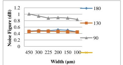
Fig. 15 is the plot of NFmin of 0.534 dB for 200 μm
transistor width and single finger with operating frequency of 3.45 GHz and gain of 11.428 dB as in Fig. 16. The two finger simulation results indicate 0.352 dB NFmin at 3.35 GHz and
gain of 12.201 dB and three finger results indicate 0.288 dB of NFmin and gain of 12.270 dB at 3.35 GHz operating
frequency for total transistor width of 200 μm. Similar results are captured for 300 μm and 450 μm total transistor width.
E. Maximum Gain Analysis of Multi-Finger Technique Fig. 16 indicates the maximum gain of 14.646 dB for 450 μm total transistor width and one finger with 1.35 GHz frequency of operation and noise figure of 1.008 dB. Two finger simulation results indicate 16.926 dB maximum gain at 1.15 GHz and 0.713 dB noise figure. Similarly 450 μm total transistor width with 3 fingers simulation results indicate 17.971 dB maximum gain at 0.95 GHz and 0.629 dB noise figure at this frequency of operation.
F. Power Report for Multi-Finger Technique
The 90 nm simulation results under 200 μm width indicate 5 mW power consumption with single finger and 8 mW power consumption for 3 finger width. Similar results are obtained for 300 μm and 450 μm transistor width under different fingers.To improve NF and gain of common source amplifier with cascodetopology can be considered. In addition the device characteristics such as carrier mobility and diffusivity can be considered for design analysis.
0.2 0.3 0.4 0.5 0.6 0.7 0.8 0.9 1 1.1
180 130 90
N
o
ise
Fi
g
u
re
(
d
B
)
Technology
66.66
150
225
Fig. 15:Noise Figure performance of LNA with different fingers NF under 200 μm, 300 μm and 450μm with three PTM models
Fig. 16:Power gain performance of LNA with different fingers NF under 200 μm, 300 μm and 450 μmwith three PTM models
IV. CONCLUSION
In this paper, the design of CS LNA with source degeneration is implemented in three different technologies such as PTM 180 nm, PTM 130 nm and PTM 90 nm models. The transistor geometry has been arrived for circuit schematic design and captured in ADS software. The simulation results obtained demonstrated that the designed LNA is suitable for Bluetooth applications of 2.45 GHz to 2.85 GHz with maximum power gain of 14.646 dB with 150 μm transistor width using PTM 90 nm technology and minimum noise figure of 0.178 dB with 300 μm transistor geometry using PTM 130 nm model technology.
REFERENCES
1. Parssinen J. Jussila, J.Ryynanen, L. Sumanenand K. Halonen, “AWide-Band Direct Conversion Receiver for WCDMA Applications,” IEEE int. Solid-State Circuits Conf., 1999, pp. 220–221. 2. M. Niroue, S. Ziabakhsh, H. Alavi-Rad and S. Ziabakhsh, “A High Conversion gain, Low Noise figure RF-CMOS receiver front-end IC for 2.4 GHz applications,” IEEE Asia Pacific Conf., on circuits and Systems, 2010, pp. 839-842.
3. Shafqat Hameed, AsimJavaid Butt, Umar Khan and Atta Badii, “Performance analysis, design and assessment of broadband Low Noise Amplifier (LNA) for radiometer,” InternationalJournal of Physical Sciences, Vol. 7, 2012, pp.2181 – 2195.
International Journal of Innovative Technology and Exploring Engineering (IJITEE) ISSN: 2278-3075, Volume-8 Issue-9, July 2019
5. Sheng Chen, Runxi Zhang ChunqSh, Yanlin Shi and Zongsheng La, “A Q-Band CMOS LNA with Common Source Topology Based onAlgorithmic Design, Methodologies,” IEEEconference ICSICT, 2014, pp. 1-3.
6. C. Lung Hsiao, Ro-Min Weng and Kun-Yi Lin, “A 0.6 V CMOS Low Noise Amplifier for 2.4 GHz application,” Proceedings of IEEE Asia Pacific Conference on Circuits and Systems, Vol. 1, 2004, pp. 277-280. 7. M.K. Salma and A.M. Soliman, “Low Voltage Low Power CMOS RF Low Noise Amplifier,” Int. J. Electron. Commun. (AEU), Vol. 63, 2009, pp. 478–482.
8. T. Sasilatha and J. Raja, “A 1 V, 2.4 GHz Low Power CMOS Common Source LNA for WSN Applications,” Int. J.Electron. Commun.(AEU).
Vol. 64, 2010, pp. 940–946.
9. D.K. Shaefferand T. H. Lee, “A 1.5-V, 1.5-GHz CMOS Low Noise Amplifier,” IEEE J. Solid-State Circuits, Vol. 32,1997, pp.745-759. 10. Ren-Chieh Liu, Kuo-Liang Deng and Huei Wang, “A
0.6-22-GHzBroadband CMOS Distributed Amplifier,” IEEE Radio Frequency Integrated Circuits Symposium,2003, pp. 103-106. 11. James Wilson and Mohammed Ismail, “Input Match and LoadTank
Digital Calibration of an Inductively DegeneratedCMOS LNA,”
Integration, the VLSIJournal. Vol. 42, 2009, pp. 3-9.
12. Kuo-Liang Yeh and Jyh-ChyurnGuo, “A New Method for Layout-De pendent Parasitic Capacitance Analysis and Effective Mobility Extraction in NanoscaleMultifinger MOSFETs,” IEEE Transactions on Electronic Devices, Vol. 58, 2011, pp. 2838-2846.
13. Gh.R.Karimi and S.BabaeiSedaghat, “Ultra Low Voltage, Ultra LowPower Low Noise Amplifier for2 GHz Applications,”
Int.J.ElectronCommun (AEU),Vol. 66, 2012, pp. 18–22.
14. S. T. Nicolson, S. P. Voinigescu, “Methodology for SimultaneousNoise and Impedance Matching in W-band LNAs,” Proc. IEEE Compound Semiconductor Integrated Circuits Symp, 2006, pp. 279-282.
15. Kusuma M.S, S. Shanthala and Cyril Prasanna RajP, “Design of Common Source Low Noise Amplifier with Inductive Source Degeneration in Deep Submicron CMOS Processes,” International Journalof Applied Engineering and Research (IJAER), Vol. 13,2018, pp. 4118-4123.
16. Predictive Technology Model, http://ptm.asu.edu
17. J.Scholten, L. F. Tiemeijer, R. Van Langevelde, R. J. Havens and A. TZegers-van Duijnhoven, “V. C. Venezia, Noise Modelling for RF CMOS Circuit Simulation,” IEEE transactions on Electronic Devices,
Vol. 50, 2003, pp. 618–632.
18. M. J. Deen, C. H. Chen, S. Asgaran, G.A.Rezvani, J. Tao and Y. Kiyota,“High-Frequency Noise ofModern MOSFETS: Compact ModelingandMeasurement Issues,” IEEE Transactions on Electronic Devices, Vol. 53, 2006, pp. 2062–2081.
19. Razavi, R.H., Yan and K. F. Lee, “Impact of Distributed Gate Resistanceon the Performance of MOS Devices,” IEEE Transactions on Circuits and Systems I: Fundamental Theory and Applications, Vol. 41, 1994, pp. 750-754.
20. Kuo-Liang and Jyh-ChyurnGuo, “Narrow-Width Effect on High-FreFrequency Performance and RF Noise of Sub-40-nm MultifingernMOSFETs and PMOSFETs,” IEEE Transactions on
Electronic Device, Vol. 60, 2013, pp. 109-106.
21. Xiaomeng Zhang, Shuo Li, Tylor Moody, HaoXue and Saiyu Ren, “Multi-finger MOSFET Low Noise Amplifier Performance Analysis,IEEE, 2014, pp. 343-345.
AUTHORSPROFILE
Mrs. Kusuma M. S. received her M.Tech degree in Digital Electronics from Visveswaraya Technological University, Karnataka, India and B.E. degree in Electronics & Communication Engineering from Kuvempu University, Karnataka, India. She is currently working as Assistant Professor at Govt. SKSJTI, Bengaluru and pursuing Ph.D in Electronics and Communication Engineering under Visveswaraya Technological University. Prior to this she worked in WIPRO Technologies as a Project Engineer where she was responsible for verification of ASIC design. She has 4 years of industry experience and more than 10 years of teaching experience. Her research interests include low power VLSI, Wireless sensor networks, Analog and Digital system design.
Dr. S. Shanthala, is working as a Professor and Head, Dept. of Telecommunication, B.I.T, Bengaluru. She has a teaching experience of about 27 years. She has presented & published many papers in several International and National Conferences &Journals. She is a life member of MISTE and MIMAPS. Her area of interest includes Low power VLSI design, Embedded systems and Digital Signal processing.
Dr. Cyril Prasanna Raj P obtained his PhD from Coventry University, UK, M. Tech from KREC Su-rathkal and BE from SJCE Mysore. He is also senior member of IEEE, and Council Member(Treasurer) IEEE Sensors Council (Bangalore Chapter).
He is working as Dean (R&D) at MS Engineering College, Bangalore. Prior to this he was at MS Ramaiah School of Advanced Studies, Bangalore as HOD-EEE Department for 12 years. He has more than 16 years of experience in teaching and research. At MSEC, Banga-lore he is also the Director for Innovation and Entrepre-neurship Development Cell funded by DST.