ISSN: 2278-3075, Volume-8, Issue-9S, July 2019
Published By:
Performance Improvement of DVFS Based 16 Bit
SAR ADC
Rinkesh Mittal, Navneet Kaur, Parveen Singla
ABSTRACT-Analog-to-digital converters (ADCs) at elevated efficiency are vital components for elevated quality image sensors growth. In order to achieve the necessary resolution at a specific velocity, these systems need a large amount of ADCs. In addition, energy dissipation has now become a main output for analog models, especially for mobile equipment. Such a circuit design is a difficult job, requiring a mixture of sophisticated digital circuit design, analog expertise and iterative design. The sharing of amplifiers was frequently employed for reducing dissipation of energy in ADC pipelines. In this paper we present the topology of a 16-bit ADC pipeline, developed in 45 nm CMOS. Its efficiency is likened to a standard Scaling configuration for amplifier and a completely shared amplifier.
Key Words— Analog-digital converters (ADC), data conversion, low power, successive approximation register architecture (SAR), digital to analog converter (DAC).
I. INTRODUCTION
The processor core, memory and programmable input and/or
output peripherals is a microcontroller or MCU. It is
easier, but more embedded than the microprocessor
(CPU). This makes it inexpensive to use and grow and
increases the amount of MCUs per human. Many MCUs
can be used in other equipment, such as automobiles,
telephones, equipment etc. The worldwide industry for
MCU is enormous and has a significant complete
importance, even though one MCU is inexpensive. The
later MCUs use more power. Therefore it becomes
increasingly essential to create energy-efficient MCUs
in order to get as long as necessary for the battery life.
We would like them to use as little energy as possible.
Revised Manuscript Received on June 15, 2019.
Dr. Rinkesh Mittal, Electronics and communication Engineering, Chandigarh Engineering College, Landran, Mohali, Punjab
Navneet Kaur, Electronics and Communication Engineering, Chandigarh Engineering College, Landran, Mohali, Punjab.
Dr. Parveen Singla, Electronics and communication Engineering Chandigarh Engineering College Landran, Mohali, Punjab
A MCU must often communicate with analog signal
detectors. The inbound data is transformed into the
MCU by an analog to digital converter (ADC) which is
recognizable by the processor.
The goal of this master thesis is a bigger concept for an
ULT microcontroller to create an energy-effective ADC.
The job was built on an earlier master dissertation,
which develops the digital construction required for a
MCU.
High sample rate and medium resolution
analog-to-digital converters are significant components of
instrumentation (oscilloscopes, spectrum analyzers,
medical
imaging),
video
apps
and
wireless
communication where pipelined ADCs are frequently
used [4] .The static power consumption of amplifiers
between converter phases is a significant disadvantage
of the pipeline architecture. ADC architectures are a
compact option with efficacy and usually intended for
fewer frequencies and are the basis for successive
approximation registers (SAR).
II. ADC COMPARATOR
To determine which of the two condenser array has the
largest voltage, a differential comparator is used. If the
favorable entry has more voltage than the adverse input,
the comparator will have an elevated voltage supply
(V
dd). The comparator yield is small if the adverse input
is greater (V
ss). A latch is used to do that. The
conventional clocked latch consists of two stages, one
monitoring stage and one lock. The first thing is to lock
the clock, but to lock it in one direction or the other.
Normally, the locking stage is started by a heavy clock.
The lock is tightened to an input and does not change
before the clock modifications and the lock is reset to
monitoring mode.
The first model of the fundamental simulations was the
comparator in Verilog A. This module was designed to
ensure that the layout functioned in its entirety and to
show how everything would be done. Features such as
setup time should be used to ensure coherence in
moment for all modules. We prevent adding noise, but
instead maintain it as an optimal
830
Published By:of this module. A fresh module was produced at the
transistor level in the second layout phase. To ensure
correct behavior, everything is simulated by cadence.
Design options parameters are most often sought and
also feasible For example, the low bias current has been
reduced from the outset and the design has been realized
to meet the needs. For beginning the concept was to
maintain all as easy as feasible, more transistors
essentially mean more stuff that can unwantedly alter
the conduct.
PMOS transistors can be used as reference transistors to
further minimize noise [6] .That is because p-channel
MOSFET Electron are less to the transistor channel than
n-channel MOSFET [6] .Fig.1: Noise summation through gain stages [4]
III. SAR BASED ADC
The subsequent ADC approval architecture uses an 1-bit binary search algorithm to draw a digital value from an analog signal [6], as shown in fig.2 ADC approximation (SAR ADC) design. The most common SAR ADC, the SAR ADC recharge, utilizes condensers to store and edit the input signal [6]. This technique discharges the condensers and allows the voltage to be split in the DAC array by a power-of-two. A sample and hold (S/H) circuit is the general architecture of the SAR ADC architecture comparative system and digital logic and it is managed by the clock, with N+1 times the sampling frequency where N is the bit resolution and additional time for the input signal sampling [ 6]. The various sections are illustrated.
In general, significant ADC parameters are split into two wide classifications: DC Input to provide a logical bit 1, 0 operation and AC Input provide (0-5v) discrete form of operation. The following requirements are detailed in this document.
fig.2: SAR Overview [3]
IV. ADC PARAMETERS
A. Dc (or static) input specifications: (a) Offset Error and drift
(b) Gain Error and drift
(c) Differential Non Linearity (DNL)
(d) Integral Non Linearity (INL)
(e) Total Unadjusted Error (TUE)
B. AC (or Dynamic) Input Specifications:
(a) Total Harmonic Distortion (THD)
(b) Signal to Noise Ratio (SNR)
(c) Signal to Noise and Distortion (SINAD)
(d) Spurious Free Dynamic Range (SFDR)
V. PROPOSED DESIGN RULE
The guidelines shall be applied to verify if the layout is right. The layout
Voltage reference
regulator (analog
model using capacitors
& resistor)
Differential
capacitor DAC
array
Comparator
(pre-amplifier,
latch & signal
rectifier
Digital control
logic (VHDL
coded arbiter)
Asynchronou
s clock
i/p
I/P
Gain stage 2 Gain
stage 1
Input
Noise
[……]
Noise stage1
ISSN: 2278-3075, Volume-8, Issue-9S, July 2019
Published By: comes to the manufacturing facility for the production after
complete checking of each rule. This method is known as the automation of electronic construction. Basically, these guidelines do not control the design of the schematic [5]. Lambda-based laws are the most common among them. Three fundamentals width, size and mask regulations are applicable. Certain laws of lambda are the following-
● Well to well spacing should be 2 χ ● Well to poly spacing should be 2 χ ● Well to metal spacing should be 3 χ ● Poly-active minimum spacing should be 1 χ ● Poly overlap spacing should be 2 χ
VI.PROPOSED ADC DESIGN ALGORITHM DYNAMIC VOLTAGE SCALING (DVFS)
Dynamic tensile scaling is a computer architecture energy management technology where the tension used in an element according to conditions, is enhanced or reduced. Overvoltage is known as dynamic voltage scaling, dynamic voltage scaling is considered under current to decrease the voltage Under voltage, power is saved, notably on portable computers and mobile devices[4], where battery-powered energy is generated and
therefore restricted, or uncommon, to improve
efficiency. Over
voltage is performed to improve the efficiency of the machine.VIII. RESULT AND SIMULATION
The trans-impedance amplifier is shown in Fig.3 in two phase push-pull converters. It is made up of two serial-connected inverters. Each inverter includes an NMOS with a diode load, which will boost the bandwidth and reduce the miller effect. A feedback resistor that is substituted by NMOS transistor was also used in the suggested ADC system as an effective resistor based on the gate voltage bias. In addition to improved controllability, implementing the feedback resistor with NMOS greatly saves chip region. In equation 1 of the following, the value of feedback resistor can be determined.
Where W =width, L = length, Vgs = gate-to-source voltage, Vt = threshold voltage and μCox= Transconductance parameter (is it the correct definition of the parameter).
Each PMOS transistor has a 1.6V voltage source Vdd implemented. Input-to-output signal amplification takes place. ADC output is provided on Vout terminal and feedback on the amplifier input is provided for part of the production.
Fig.3 Circuit diagram Of Proposed cell of ADC.
The above figure shows two case cade connected MOS circuit with also work as a similar to current amplification technique and that is enhancement of all circuit Tran’s impedance.
Two-Stage Trans impedance Amplifier consists of three identical stadiums with 7 NMOS transistors and 3 PMOS. The circuit uses a photocurrent of 3μA. The feedback transistor is biased by a dc voltage of 1.3V. To make them work as amplifiers, the transistors should be located in the saturation region with the exception of the feedback transistor, which is used as a resistor in a linear region.
The simulation is conducted using the DSCH Spectrum Simulator. The simulator uses CMOS technology of 45 nm. ADC calculations: the profit from the Trans impedance amplifier is indicated by the voltage proportional to the input current, as described previously. The single phase ADC increase is achieved,
A= gm13 + gm 20 + gm 15... (3)
The cube of the single phase ADC is made to calculate the profit from three phase ADC. The reason is that the ADC phases are linked in sequence,
which multiplies the profits for all phases. Since all phases are the
)
1
..(
...
) (Vgs Vt C W
L
832
Published By: remains the same and the overall gains in ADC. The increasein the suggested ADC is shown in Fig 6.
Calculation of the ADC capacity: The ADC range of 3 dB shall be calculated at the 3 dB decrease point. One of the most significant factors in the design of an ADC is the bandwidth improvement. The improvement of bandwidth is performed through the correct choice of the value of the MOS attached to the diode. The bandwidth can be calculated mathematically with a form-
[image:4.612.333.548.52.271.2] [image:4.612.62.245.412.579.2])
4
..(
...
2
1
RfC
A
Bandwidth
Where A is the gain, Rf is the feedback resistance and C is the capacitance. The bandwidth thus calculated is obtained as 371.32 MHz Fig. 4 shows the bandwidth of proposed ADC. Calculation of ADC noise and power: The input noise referred to here is calculated are generally by input sources. The resulting waves will not indicate the effects of the input sources on the machine (with open circuits for the present sources, and with brief circuits for voltage controls). This noise will therefore not indicate the impact of the input sources on the machine. The calculated noise can be achieved as 0.827 dramatic noise / total Hz. The noise of the ADC suggested is shown in Fig 3. The device's energy dissipation should be as small as feasible. The wasted DC power here is 0.871mW.
Fig.4 Circuit diagram Of Proposed case cade ADC.
Figure 4 Proposed ADC design: the design of the suggested ADC is produced with the DSCH Software after assessment and calculations are completed. The suggested ADC is presented in Figure 4.
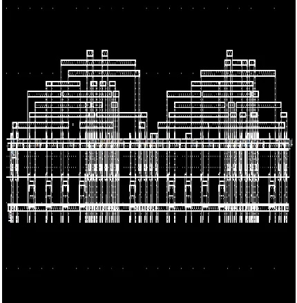
Fig.5 Layout of Proposed ADC circuit
In the above figure, MICROWIND output to design of layout of use of design rule nanometer technology. This is also improving of frequency and reduction of all circuit power and reverse current.
Fig.6 shows the gain margin (10.02 dB) and phase margin (1.4 deg), displayed in the title, are marked with solid vertical lines. The dashed vertical lines indicate the locations of Wcg, the frequency where the gain margin is measured, and Wcp, the frequency where the phase margin is measured.
ISSN: 2278-3075, Volume-8, Issue-9S, July 2019
Published By: Fig.6 Gain of Proposed ADC
834
Published By:
In 45 nm CMOS technology, the pipeline SAR
ADC can be applied using EDA tools. The
simulation findings show that a 16-bit monotonic
high-speed
transformation
is
possible.
This
instrument is suited for the conventional VLSI
application of CMOS technology. This ADC is
particularly used in biomedical apps with small
frequency.
REFERENCES
[1] T.Sowmya, SK. Muneer Nihal, “IMPLEMENTATION OF 16-BIT PIPELINED ADC USING 180nm CMOS TECHNOLOGY”, International Research Journal of Engineering and Technology (IRJET) e-ISSN: 2395-0056 Volume: 05 Issue: 03 | Mar-2018 www.irjet.net p-ISSN: 2395-0072.
[2] Saima Bashir, Samiya Ali, Suhaib Ahmed, “Analog-to-Digital Converters: A Comparative Study and Performance Analysis”, International Conference on Computing, Communication and Automation (ICCCA2016),2016.
[3] T. Moody, "Design of a 10-bit 1.2 GS/s Digital-to-Analog Converter in 90 nm CMOS," Ohio LINK Electronic Theses and Dissertations Center., 2015.
[4] Abhishek Rai, B Ananda Venkatesan,“Analysis and design of High Speed and Low Power Comparator in ADC”, International Journal of Engineering Development and Research (IJEDR), 2014.
[5] S. Ren and J. Emmert, "Successive approximation pipelined ADC with one clock cycle conversion rate," The Institute of Engineering and Technology 2012 ELECTRONIC LETTERS, vol. 48, no. 20, 27th September 2012.
[6] Baker, R. Jacob. CMOS: circuit design, layout, and simulation. Vol. 18. John Wiley & Sons, 2011.
[7] M. a. A. Zeki, "Current-steering digital-to-analog converters: functional specifications, design basics, and behavioral modeling," Antennas and Propagation Magazine, p. 197– 208, 2010.
[8] I. -H. Wang, J. -L. Lin and S. -I. Liu, “5-bit, 10 G Samples/s track-and-hold circuit with input feed through cancellation," Electronics Letters, vol. 42, no. 8, pp. 457 - 459, 2006.
[9] Oskuii, SaeeidTahmasbi. "Comparative study on low power high performance flip-flops." (2004).
[10] P. E. Allen and D. R. Holberg, CMOS analog circuit design., Oxford Univ. Press, 2002.
[11] Rossi, A., and G. Fucili. "Non redundant successive approximation register for A/D converters." Electronics letters 32.12 (1996): 1055- 1057.
[12] F. Kuttner, "A 1.2v 10b 20MSample/s non-binary successive approximation ADC in0.13um CMOS," in IEEE International Solid-State Circuits Conference, 2002. [9] B.Razavi, Principles of Data Conversion System Design, IEEE Press, 1995.
[13] Yee, Y. S., L. M. Terman, and L. G. Heller. "A two- stage weighted capacitor network for D/AA/D conversion." SolidState Circuits, IEEE Journal of 14.4 (1979): 778-781.
[14] J. McCreary, "Successive Approximation Analog to Digital Conversion Techniques in MOS Integrated Circuits," University of California, Berkeley, 1975.
[15] Ian Beavers contributing technical expert, "Understanding Spurious-Free Dynamic Range in Wideband GSPS ADCs by Ian Beavers,," Analog Devices, Inc. Technical Article MS-2660.
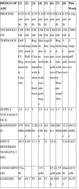
DESIGN OF
ADC
[1] [2] [3] [4] [5] [6] [7] [8] This
Work
PROCESS 0.25
μm Si 0.35 μm Si 0.35 μm Si 0.18 μm Si 0.35 μm Si 0.35 μm 0.18 μm Si 0.35 μm Si 0.16μ m TECHNOLO GY CM OS CM OS CM OS CM OS CM OS CM OS CM OS CM OS CMO S
TOPOLOGY Diff
erent AD CI Reg ulate d Casc ode 1 stage push Pull inver ter Reg ulate d Casc ade input with shun t feed back Shu nt-shu nt feed bac k with casc ode gain stag e regu late d casc ode 5-stag e pus h pull inve rters Reg ulate d casc ode with Cher ry- Hoo per ampl ifier 3-stag e push pull inve rters 2-stage push pull invert ers SUPPLY VOLTAGE(V OLT)
2.5 3.3 3 3.5 3.3 3.3 1.5 3.3 1.2
BANDWIDT H 670 MHz 910. 5MH z 2.2G Hz 1.8 GH z 6G Hz 10G b/s 280 MHz 12.5 MH z 401.0 0MH z INPUT REFERRED NOISE(PA/√ HZ)
20.9 6.03 17.1 9 21 25.8 - 3.54 0.827
CONSUMPTI
ON
27m
W
- - 115
mW
- 87.4
mW 1.57 mW 60m W 0.871 mW
GAIN(DB) 80 69.7 55 64 51 36.5
6
99 107.
3
[image:6.612.73.334.80.697.2]ISSN: 2278-3075, Volume-8, Issue-9S, July 2019
Published By:
AUTHOR”S PROFILE
Navneet Kaur was born in Punjab, on 13th september, 1992.
She persuade her diploma in electronics and communication from Kurukshetra University, India in year 2011 and B.tech in Electronics and Communication engineering in 2104 from himachal university, 2014. Currently, she is persuing Mtech in VLSI Design from PTU University. The research interest of her includes DVFS based ADC.
Dr. Rinkesh Mittal is Professor in Electronics and Communication Department .He has 15+ years of vast teaching experience. He has completed B.Tech, M.Tech. M.B.A. and PhD. His research areas include Wireless Communication,VLSI & Antenna .He has filed patents & published 50 +International Journal papers.
Dr. Parveen Singla did B.Tech in Electronics and Communication Engg. from Hindu college of Engineering, Sonepat affiliated to Maharishi Dayanand University, Rohtak in 2003 and M.Tech in Electronics and Communication Engg from N.C College of engineering, Panipat affiliated to Kurukshetra University, Kurukshetra in 2008. He did PhD in ECE from IKGPTU in 2016. His total teaching & research experience is 10 years. Now he is working as Assoct.. Prof. in Electronics & Communication department in Chandigarh engineering college. He has more than 20 publications in various reputed journal/conferences. His research area includes wireless communication and soft computing.