City, University of London Institutional Repository
Citation
:
Fréchette, M. F., Vijh, A., Utracki, L., Trudeau, M. L., Sami, A., Laurent, C., Morshuis, P., Andritsch, T., Kochetov, R., Vaughan, A., David, E., Castellon, J., Fabiani, D., Gubanski, S., Kindersberger, J., Reed, C., Krivda, A., Fothergill, J., Dodd, S. J., Guastavino, F. and Alamdari, H. (2010). Nanodielectrics: A panacea for solving all electrical insulation problems? In: 2010 10th IEEE International Conference on Solid Dielectrics (ICSD). (pp. 1-29). IEEE. ISBN 978-1-4244-7945-0This is the accepted version of the paper.
This version of the publication may differ from the final published
version.
Permanent repository link:
http://openaccess.city.ac.uk/7094/Link to published version
:
http://dx.doi.org/10.1109/ICSD.2010.5568067Copyright and reuse:
City Research Online aims to make research
outputs of City, University of London available to a wider audience.
Copyright and Moral Rights remain with the author(s) and/or copyright
holders. URLs from City Research Online may be freely distributed and
linked to.
City Research Online: http://openaccess.city.ac.uk/ [email protected]
Nanodielectrics
A Universal Panacea for Solving All Electrical Insulation Problems ?
by an international collective of scientists*
Prologue
At times new paradigms are observed to emerge. One example of this concerns the introduction of the concept of “Nanodielectrics” in 2001. It is often demeaned that with new concepts must come new ways of thinking, opened-minded consideration and un-bounded exploration. In this spirit, an activity of high-creative in-tensity was organized at Hydro-Québec’s research institute (IREQ) on October 31st, 2008. A very diversified crowd of international scientists gathered at IREQ to exchange and reflect on the topic. An opportunity to be seized to break the established precincts and, to question and imagine the potentialities.
Provocative at times, the comments and views were only meant to elicit the progress of our thinking. The present paper does not summarize the proceedings of the event that came to be known as the “Brainstorm at the institute”. This paper offers a broad and diverse view of the topic, with many remaining questions of impor-tance and feeded by recent progress and further reflection. Al-though long, the paper gives a vivid picture of the situation allow-ing criticism and stressallow-ing the many unanswered questions. Multid-isciplinary zest is obvious.
Most of the participants joined in this new adventure. The list of authors is given at the end with an indication of their respective contribution. In view of the great number of authors, no effort was undertaken to reconcile the styles. The end product is a result of a participatory effort, and every bit does not need to be guarantied and accepted by all.
The paper benefited particularly from the contributions of some scientists stranger to the usual field, namely A. Vijh, L. Utracki and H. Alamdari. AshokVijh joined us with his background in electro-chemistry and has enlightened us with analogies of other fields concepts and applications (Chapter II). Leszek Utracki, a polymer scientist of many talents, has taught us by linking the polymeric context of nanocomposites to the dielectric properties. He has pro-duced Chapter III. This would have been a logical determining cobblestone just after the introduction of the concept in 2001. This somewhat warranted a welcomed longer contribution. Finally, Houshang Alamdari is back in the mist of academic research. He was associated with the nanodielectrics from the beginning. For this paper, he introduced a non-electrotechnical application based on a nanodielectric material (Chapter VIII, section B).
Michel F. Fréchette, Varennes, March 2010
IREQ - 40 ans de savoir et d’énergie
Nanodielectrics; polymer nanocomposites; electrical insulation; solid dielectrics
I. NANODIELECTRICS
When the nanodielectric concept was introduced [1] in 2001, it stemmed from a reaction to the great stir surrounding the nanostructuration of crystalline materials. What was in it for the insulation arena? Was there an equation of the sort “Nanotechnology + Dielectrics” equals something like a nano-material with affected dielectric properties?
Already, towards the end of the 90s, we had identified the aerogel and variants as 3-dimensional nanodielectrics. Also, some works pointed at nanoceramics exhibiting peculiar behav-iours. Despite the fact that upon sintering, nanometric-size grains grow in dimensions, particular effects if not benefits from initial mixtures into ceramics of nanocomponents and additives had emerged. The major step taken in 2001 was pro-posing special dielectricity for polymer nanocomposites. A dielectric behaviour shaped, dictated or affected from a nano-scale manipulation. An account of the development of the cept was published last year [2]. In the emergence of the con-cept, the seminal work by John Lewis was recognized. Dielec-tricity at the nanoscale is thought to play a major role in deter-mining the macroscopic upscale of the phenomena.
Although so far a major research effort has taken shape on nanodielectrics, it was dominated by the influence of polymer nanocomposites. In this framework, interfaces (as well ex-plained by Lewis [3]) are dominant. However, the concept of nanodielectric [4] is more general than this. Eventually, when the degree of self-assembly will be mastered, insulating solids of revolution including polymers shall be constructed in which interfaces as well as building blocks will interplay.
A nanodielectric is by definition “a multi-component di-electric possessing nanostructures, the presence of which lead to changes in one of several of its dielectric properties”. The novelty is still in its infancy. Potentiality has been blurred for instances by the quality control of the polymer nanocomposites and/or the effects of sintering involving nanoceramics. But the future is ahead. Despite the difficulties, partial nanostructura-tion of polymer nanocomposites were found to improve partial-discharge resistance, to suppress space charge formation and affect charge relaxation, and to prolong the treeing lifetime [5, 6]. Many times, it remains a mystery how to change many properties at the same time. Especially considering that for an electrotechnical application, the material must satisfy a matrix of properties. Many of these properties are not dielectric.
scrutiny, there is evidence for an electrical microstructure con-sisting of semiconducting grains and insulating grain bounda-ries. It would seem that the low-achieved degree of self-assembly [8] for now precludes the observation of more novel-ties. In this direction, progress in the design and use of den-drimers [9] and, for instance, new techniques of sintering at low temperature (see for instance in [10]) will be instrumental in the near future.
For the next steps of development, force is to mention that nanofillers exhibiting extraordinary properties will draw some more attention. It is one of the approaches in order to provoke real emergence of novelty and/or marked deviations from ex-trapolated property improvement. To mention a few, carbon nanotubes [11] with or without encapsulation, silica flakes or graphene planes [12], insulating nanotubes like Boron Nitride [13] fall into this category. It is an area of research that shows promises.
The future lies ahead. The wealth of information on so many aspects presented in the following sections points indeed at the existence of a future for the field involving the nanostruc-turation of dielectrics.
[1] M.F. Fréchette, M. Trudeau, H.D. Alamdari and S. Boily, “Introductory remarks on nanodielectrics,” Proc. IEEE Conf. on Elect. Insul. and Di-elec. Pheno., Kitchener, Ontario, Canada, Oct. 14-17, 2001.
[2] M.F. Fréchette, “Innovation in dielectric materials : from macro to nano-scales”, Invited talk, Electr. Insul. Conf., Montréal, Juin 2009.
[3] T. J. Lewis, “Interfaces are the dominant feature of dielectrics at the nanometric level”, IEEE Trans. Dielectr. Insul., Vol. 11, pp. 739-753, 2004.
[4] M. F. Fréchette, M. L. Trudeau, H.D. Alamdari, and S. Boily, “Introduc-tory remarks on nanodielectrics”, IEEE Trans. Dielectr. Electr. Insul., Vol. 11, pp. 808-818, 2004.
[5] M.F. Fréchette, C.W. Reed, and H. Sedding, “Progress, understanding and challenges in the field of nanodielectrics”, IEEJ Trans. Fundamentals and Materials, Vol. 126, No. 11, pp. 1031-1043, 2006.
[6] T. Tanaka and M. Fréchette, Eds., “ Emerging nanocomposite dielec-trics”, CIGRÉ, TF D1.16.03 Task force report, Electra, 2006.
[7] M.C. Ferrarelli, D.C. Sinclair, A. R. West, et al. “Comment on the ori-gin(s) of the giant permittivity effect in CaCu3Ti4O12 single crystals and ceramics”, J. Mat. Chem. , 19, 5916-5919, 2009.
[8] M.F. Fréchette and C.W. Reed, “On molecular dielectrics in their role of shaping and controlling nanodielectrics”, IEEE Conference on Electrical Insulation and Dielectric Phenomena, to be held in Kansas City, USA, October 15-18, 2006.
[9] Jean M.J. Frechet and Donald A. Tomalia, “Dendrimers and Other Den-dritic Polymers ” , J. Wiley & Sons, 2001.
[10] M.F. Fréchette, R.Y. Larocque, M. Blouin, and S. Boily, “Nanophase semi-conductive ceramics: Dielectric surface performance when exposed to charges“, Conference on Electrical Insulation and Dielectric Phenom-ena, Boulder, Co USA, October 17-20 2004.
[11] Xiao-Lin Xie, Yiu-Wing Mai, Xing-Ping Zhou, “Dispersion and align-ment of carbon nanotubes in polymer matrix: A review”, Materials Sci-ence and Engineering R 49, 89–112, 2005.
[12] M. I. Katsnelson, “Graphene : carbon in two dimensions”, Materials Today, , Vol. 10, No. 1-2, pp. 20-27, Jan-Feb 2007.
[13] M. Ishigami, Shaul Aloni, A. Zettl, “Properties of Boron Nitride Nano-tubes”, in Proceedings of 12th International conference on scanning tun-neling microscopy /spectroscopy and related techniques, vol. 696 of AIP Conference Proceedings (American Institute of Physics, Melville, NY), p. 94, 2003.
II. SOME PHYSICOCHEMICAL CONSIDERATIONS ON NANOMATERIALS INCLUDING NANODIELECTRICS
Nanotechnology is the new growing frontier involving most areas of science and engineering. Almost every country has some sort of national nanotechnology initiative.
Nanotechnology is the research and development at the atomic, molecular or macromolecular levels in the sub-100 nm range ( 0,1 - 100 nm) to create structures, devices and sys-tems that have novel functional properties. Other definitions of nanotechnology have also been proposed but they all focus more or less on the 0,1 - 100 nm range with some variations which are not central to the present discussion.
Nanomaterials are thus defined as the substances and con-stituents, invariably solids, which are used to make the devices and structures in the 0,1-100 nm range. Such nanomaterials possessing interesting and useful dielectric properties are called nanodielectrics, which are the focus of the present re-view. These are invariably solid materials and are usually used as composites in which a small quantity of nanoparticles of one material (e.g. an oxide) is embedded within the main body of another dielectric material, e.g. a polymer.
A. Basic Physicochemical Nature of a Nanomaterial and its
Consequences
A nanomaterial is dominated by the presence of grain boundaries over grains, i.e. over fifty percent of the solid is constituted by line defects (i.e. grain boundaries) and these interphasial regions (between the grains) are constituted by atoms having bonding (lower coordination number) that leads to high surface energy, high reactivity, low stability (e.g. ten-dency to sinter under high-field or temperature conditions), easy precipitation of impurities, strong chemisorption, and higher ionic conduction, etc. than the grains.
Importantly, novel functional properties arise in such mate-rials owing to their nanosize; such properties usually have their origins in quantum mechanical effects which exhibit themselves at such levels of miniaturization. Thus “nano” does not just denote “miniaturization” – such miniaturization must lead to novel functions and properties. For example, when a nanomaterial particle approaches lower size limit of around 40 Å, quantum mechanical effects dominate creating totally new material properties, e.g. Pt particles of that size exhibit a pseudo band-gap and thus reduced electron density and cata-lytic properties. Gold particles of that size, on the other hand, show higher catalytic activities for reasons not altogether clear at the present time, although it may have to do with the spd hybridization under quantized conditions. In semiconductor quantum dots and quantum wells, the quantum confinement of electrons and holes arises at the nano-level which gives rise to novel device properties.
cur-rents pass; this, of course, is a quantum effect. A more spec-tacular example which is extremely speculative, is the basis of consciousness: how a piece of meat (i.e. brain) thinks? At the microtubules level in the neurons and other brain tissues, there are quantum transfer events at the nano and sub-nano scales, e.g. work of Roger Penrose [1] at Oxford University and Stu-art Hameroff [2] at the University of Arizona (Tucson) and that of Litt [3].
B. Nanomaterials as Nanodielectrics: Problems and Promise
The reactive grain boundaries that dominate a nanomate-rial including a nanodielectric would be expected to lead to pronounced heterogeneity of the material with the following consequences (as dielectric materials) : i) high frequency dis-persion; ii) high leakage currents; iii) high dielectric loss; iv) accelerated « ageing », i.e. deterioration of dielectric proper-ties with time owing to temperature, field or current induced sintering; v) tendency to adsorb impurities and their precipita-tion at the reactive sites.
On the other hand, high reactivity of these materials would herald their use in: sensors; catalysts (gas phase reactions); electrocatalysts as in fuel cells, batteries, photoelectrochemical cells, super capacitors; pollution control devices, etc.
However, their use as dielectric materials as such would be limited because of expected high leakage currents and dielec-tric losses.
Notwithstanding these limitations, a great deal of work is being carried out in formulating composite insulating materi-als of commercial interest in which particles of nanodielctrics are embedded within a commonly used dielectric material such as polyethylene. For example, the group of L.S. Schadler at RPI in the USA has found that such a procedure yields insu-lating materials having improved breakdown strength, both at room temperature and at elevated temperatures. Other workers have also made similar observations [4,5]. What is the origin of this improved breakdown strength?
To understand the conceptual foundations of such an im-provement, it is important to observe first that the percentage of embedded nanoparticles must be quite low (1%). This is because of the low nanoparticle percolation threshold [4], par-ticularly for the commonly-used particles. If the nanoparticle content increases beyond the percolation threshold, the nanoparticle tends to loose its beneficial effects. This arises because the nanoparticles act as a sort of hindrance to the propagation of electron avalanches found during dielectric breakdown, below the percolation threshold limit; this hin-drance tends to be short-circuited above the threshold limit.
That the nanoparticles behave as barriers for electron propagation can be looked at from different conceptual angles as follows:
1) Nanoparticles because of their extended surface area change the very nature of the polymer, alter the depth and den-sity of trap sites in the language of solid state physics, thus reducing charge carrier mobility and energy.
2) The structure between the polymer and the nanoparticle is the key to the trapping mechanism; this is where the charge
layer (the “double layer” – see below) develops and nanoparti-cles present an elongated scattering path to the charge carriers. 3) Since the area of interfaces between the nanoparticles and the polymer is very large, the whole polymer matrix may be essentially treated as the interfacial region. The outcome is a set of strengthened nanometric double layer interfaces [5]. These are electrochemical interfaces within which the highest fields can be sustained [5].
Finally, the most fundamental issue is that nanoparticles embedded (distributed) in a dielectric matrix create an enor-mous number of nanoscopic electrochemical interfaces and the interphasic regions thus created determine most, if not all, the features of nanodielectrics. The most notable feature thus de-veloped is the enhancement of dielectric strength (or break-down voltage in engineering jargon). However, one would also expect other concomitant effects such as higher dielectric losses, leakage currents, ageing effects associated with “elec-trolytic” migration of charged particles and other effects from a system in which heterogeneity has been deliberately intro-duced and electrochemical double layers have been purpose-fully developed.
[1] R. Penrose, “Shadows of mind”, Oxford University press, 1994. [2] S.R. Hameroff, “Is the brain a quantum computer”, Cognitive science,
Vol. 31, pp. 1035-45, 2007.
[3] A. Litt et al., “The brain is both neurocomputer and quantum computer”, Cognitive science, Vol. 30, pp. 593-603, 2006.
[4] M. G. Danikas and T. Tanaka, “Nanocomposites – A review of electrical treeing and breakdown”, IEEE Electrical Insulation Magazine, 25 (#4), pp. 19-25, July-August 2009.
[5] T.J. Lewis, “Interfaces: Nanometric dielectrics”, J. Phys. D : Appl. Phys., Vol. 38, pp. 202-212, 2005.
III. DIELECTRIC PROPERTIES OF POLYMERIC NANOCOMPOSITES
This section describes the components of polymeric nano-composites (PNC), how these are prepared and what elements of their structure impact on dielectric properties. There are three principal PNC ingredients: polymeric matrix, nanoparti-cles and intermediary components, labelled as intercalants, surfactants, compatibilizers, etc.
A. PNC Components
1) Polymeric matrix.
From the growing concern for the environment comes a need for polymer recycling, what leads to a progressive re-placement of thermosets by thermoplastics. This tendency first affected the classical composites (e.g., epoxy/glass fiber), then polymer blends and now the PNC [1, 2]. Accordingly, this text will emphasize the PNCs based on thermoplastics, especially on polyolefins (PO) such as the commodity polyethylenes (PE) and isotactic polypropylene (PP). These polymers are semi-crystalline with relatively low melting point and may be processed at temperatures, T ≤ 250oC. PO’s are inexpensive,
2) Nanoparticles.
In the IUPAC nomenclature, the nano-sized particles must have at least one dimension in the nano-meter range≤ 2 nm. The nanoparticles may be one-, two-, or three-dimensional, but the industrial interest focuses on one-dimensional thin plates with much larger lateral dimensions [3]. These are mainly clays with platelets 0.7 – 2.5 nm thick [4]. Recently, layered double hydroxides (LDH) have been introduced [5].
The most frequently used are natural phyllosilicate clays. These are made of one octahedral layer (Oc) sandwiched be-tween two tetrahedral (Tc) ones, e.g., montmorillonite (MMT), hectorite (HT), or saponite (ST). Neither the chemical compo-sition nor the crystalline structure of clay is constant. Con-taminating atoms enter into the layers modifying clay proper-ties. For example, in MMT substitution of Al+3 in Oc by Mg+2
introduces 0.25 to 1.2 negative charges per unit cell (the cation exchange capacity, CEC ≈ 0.5 to 2 meq/g) and a commensu-rate number of exchangeable cations, which are essential for the clay ability to fully disperse (exfoliate). If Al+3 are
re-placed by Fe+3 there is no change of electron balance, but the
clay color changes what in turn results in brownish PNC. In addition to natural clays, a variety of synthetic and semi-synthetic clays have been used. The prime advantage of these materials is control of purity and stability of their chemi-cal composition. They also can be in situ interchemi-calated, avoid-ing a cumbersome step. The PNC containavoid-ing synthetic clay are white and can be dyed to any color and its intensity [4].
Little is known about the size, shape of individual clay platelet, their distribution, variability of chemical composition and impurities. Next, a short summary of results obtained by the VAMAS TWA-33 summarizes the present knowledge.
a) Shape, size and size distribution of clay platelets.
The three orthogonal dimensions of clay platelet are thick-ness (t ≈ 1 nm), length (L) = the longest platelet dimension and perpendicular to it width (W). For the tested clays the ratio:
L/W≈ 1.5 ± 0.2, thus one may discuss only L. In natural clays
L follows the Gaussian distribution with mean value ≈ 290 nm. For synthetic and semi-synthetic clays this dimension is significantly larger, viz. 1200 and 870 nm, respectively [6].
b) Chemical composition of clays.
The chemical composition of clay particles was measured using the energy-dispersive X-ray spectroscopy (SEM-EDS). Because clay may have locally-diverse composition, it is im-portant that the measurements are repeated at least 30 times per specimens. The statistical error of the chemical composi-tion in natural and synthetic clay was found to range from10 to 5% of the mean value [7].
c) Impurities.
Natural clays are contaminated by organic (humic) sub-stances, non-expandable clays (e.g., amorphous clay, vermicu-lite, kaolin) and diverse particulate minerals [1]. For the use in PNC they are laboriously purified in about 300 steps. How-ever, according to the pertinent patent, the resulting sodium clay still contains up to 5 wt% of impurities (amorphous sili-cates, stacks of welded platelets and the residual solid particles
with diameter > 300 nm) [1, 8]. The commercial, purified clay has 7 wt% of organics, hygroscopic and bound water, carbonic acid, etc.
Two clays have been analyzed for impurities; the natural sodium-MMT (Cloisite®-Na, or C-Na for short) and
semi-synthetic fluoromica (Somasif ME100). In C-Na 13 mineral contaminants were found: Vermiculite, Quartz, Cristobalite, Rutile, Albite, Microcline, Aragonite, Vaterite, Dolomite, Gypsum, Anhydrite, Alunite, Sylvite. Production of ME100 starts with natural talc and sodium fluoro silicates. In the semi-synthetic fluoromica small quantities of Vermiculite and Gyp-sum were found, probably brought in with talc [9].
3) Intercalants and Compatibilizers [1].
After purification the clay sodium salt is highly hydro-philic and as such it may be exfoliated in water, forming ther-modynamically miscible PNC with such water-soluble poly-mers, as polyethylene oxide, polyvinyl alcohol or polyvinyl pyridine; unsuitable for dielectric applications. As already mentioned, the preferred polymers for such use are hydropho-bic PO’s, PE or PP, which are thermodynamically immiscible with clay. The problem may be resolved by converting sodium clays into hydrophobic organoclays by reacting it with suitable intercalant. When this modification is insufficient for miscibil-ity, the system may be compatibilized.
Most commercial intercalants are ammonium salts, Ri4N+Cl- where Ri are organic groups, some of which should
be miscible with the polymer. For PNC with PO-type matrix, the clay may be intercalated with di-methyl di- hydrogenated tallow ammonium chloride (2M2HT) such as Cloisite® 20A
(C20A). The tallow radicals (from beef fat) are long paraffinic and olefinic chains. After hydrogenation, the saturated chains (~65% C18, ~30% C16 and ~5% C14) are expected to be
misci-ble with low molecular weight PO.
In addition to making the clay hydrophobic, intercalation also expands the interlayer spacing (from about 1.2 up to ca. 3 nm) facilitating inter-diffusion of macromolecular chains, which results in enhanced platelets dispersion. For maximiza-tion of the interlayer spacing, one may use stoichiometric quantity of intercalant having large Ri groups. However, since
these may block access to polymer molecules, the prefer strat-egy is the use of excess of intercalant. This stratstrat-egy also has negative aspects as it increases PNC degradability and con-ductivity, decreasing modulus.
Since the PNC ingredients are polydispersed, the polymer-organoclay interactions are influenced by many factors. Only using molecular simulation one may determine the effects of a single factor. Thus, simulation indicates that the ionic charges are not located in specific points of clay platelet surface, but rather they are delocalized, smeared over large areas. Conse-quently, the intercalant is also spread on the surface at thick-ness dependent on its quality and quantity [10].
of PO as that forming the matrix. Molecular simulation shows that efficiency of the process depends on the concentration, molecular weight and \compatibilizer type [11, 12].
B. Preparation of PNC Samples for Dielectric
Mea-surements
1)Compounding.
The clay-containing PNC have been prepared by the fol-lowing methods (in chronological order):
• Reactive (in situ polymerization by polymer manu- facturers)
• Solution (dispersing the organoclay in a polymer so- lution)
• Melt compounding (by compounders and part- makers).
Melt compounding is the preferred method that was used for the preparation of PNC samples for dielectric tests.
The three PNC ingredients are listed in Table I. PP has been used frequently in power capacitors, cable insulation, and in layer and phase separators for rotating electrical equipment and in transformers [13]. Polybond 3150 (PP-MA), was the compatibilizer. The organoclay C-20A is Wyoming MMT intercalated with 2M2HT.
The master batch (MB) method of compounding has been selected [14]. Accordingly, PP with 20 wt% PP-MA compati-bilizer was dry-blended with Ciba antioxidant, Irganox B-225. The composition was fed from the main hopper to a co-rotating twin-screw extruder (TSE) while 10 wt% of organo-clay was supplied from a side feeder. The materials were compounded under blanket of dry N2 at T = 200oC, screw
speed N = 200 rpm and throughput Q = 5kg/h. The MB was palletized for the use in the subsequent dilution step, which reduced the organoclay concentration to 0, 1, 2 and 4 wt%. The weight ratio of the compatibilizer-to-organoclay content was kept constant at 2:1.
2)Formation.
The PNC samples for dielectric test need to have uniform thickness of 135 ± 5 m and smooth surface. The following two-step forming method was selected. First, diluted PNC compositions were extruded at T = 180 – 230oC into blown
films. Next, these were flattened in a 3-rolls calender at 115oC.
Table I. PNC ingredients
Component Trade name Mw
(kg/mol)
Density
(g/mL) (T°C) m Supplier
PP ProFax
HL-451H (PP) 250 0.902 ~161 Polyolefins Basell
Maleated-PP Polybond 3150 (0.5%
MAH)
330 0.91 ~164 Chemtura Corp.
Organoclay Cloisite® 20A,
C-20 --- --- --- Southern Products Clay
3) Clay dispersion.
Three methods were used for assessing the degree of clay dispersion in the PNC films: the X-ray diffraction method (XRD), the Field Emission Gun Scanning Electron Micros-copy (FEGSEM) and the transmission electron microscope (TEM). XRD measures d001 – the interlayer spacing in
regu-larly spaced clay stacks. However, it does not “see” the indi-vidual clay platelets or those in twisted or deformed stacks. For this reason the additional electron micrographs of different magnification are essential.
For PNC with isotactic PP as the matrix, the interlayer spacings is small, d001 = 3.00 – 3.72 nm, decreasing with
con-centration. The micrographs show that most clay is in short stacks of intercalated platelets, thus the desired random disper-sion of exfoliated platelets was not achieved. However, it is noteworthy that PP is highly crystalline polymer in which the clay platelets are concentrated in the non-crystalline regions, where high concentration decreases the interlayer spacing. It was shown that the interlayer spacing linearly decreases with increasing organoclay content (C15) and crystallinity, (X), both in wt%, viz.:
d001 (nm) = 10.5 – 0.392 C15 – 0.111 X (1)
Accordingly, the interlayer spacing in amorphous PP ex-trapolated to infinite dilution should be fully exfoliated [15].
C. Example of the PNC Dielectric Properties
Various electric and dielectric test methods have been used in the preliminary studies of the clay effects in the PP-based PNC conducted within the VAMAS TWA-33 research pro-gram. These included space charge distribution measurements using the Pulsed Electro-Acoustic (PEA) method, the short-term electrical aging effects on breakdown strength (EBD) by
applying a ramp AC or DC voltage of 400-500 V/s to the specimen placed in silicon oil, DC polarizability and conduc-tivity measurements at -10 kV/mm for detecting the charging and discharging currents, dielectric loss at power frequency using several types of ultra precision capacitive bridges for wide frequency (0.01 mHz – 20kHz), electroluminescence emission (EL), partial discharge resistance measurements, electrical erosion tests, etc. [16-22].
1) Space charge vs. clay content and aging time.
The total quantity of charge as function of aging time, ta =
0 – 500 hrs is displayed in Figure 1.
In the case of neat PP, the homocharge injected from both electrodes accumulated in the central area, increasing with aging. In the case of PNC with 2 or 6 wt% organoclay, the heterocharges formed in the vicinity of both electrodes, ini-tially increasing with aging time and then stabilizing.
Figure 1. Charge vs. aging time for PNC containing 0, 2 and 6 wt% organo-clay [17, 20].
2 wt% organoclay. However, after aging for 360 hrs its value became similar to that in PNC with 2 wt%. Thus, PNC might be advantageous for the use in high voltage capacitors and transformers, which operate at high electric fields [17, 20].
2)Breakdown (BD) tests.
Immersed in oil film specimens were placed between a large circular, grounded electrode and a small high voltage one. For dc tests the positive voltage was increased at a rate of 90 V/s, while for ac tests the voltage was increased at a rate of 70 Vrms/s until breakdown [16, 18, 21]. Incorporation of clay
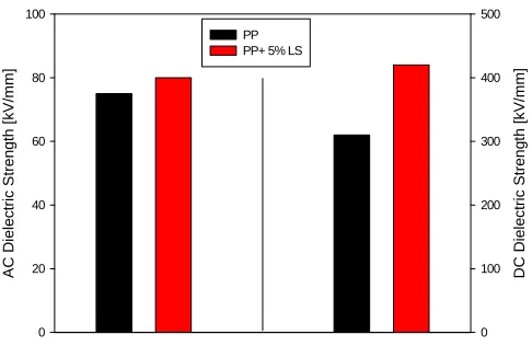
platelets in PP increased the ac and dc breakdown strength. The effect could be due to the reduction of spherulites size, caused by clay nucleation. Charges could be trapped at the interfaces reducing the probability of breakdown. Taking into account the experimental error, the incorporation of 2 or 4 wt% organoclay increased the BD strength by the same amount. However, while in ac BD increased from 116 for PP to 134 (± 10) kVrms/mm for PNC’s; in dc the change was more
substantial (from 354 ± 85 to 488 ± 130 kV/mm). Thus incor-poration of nanoparticles increased the breakdown strength by 15 and 38% in ac and dc field, respectively.
Bulinski et al. studied PP-based PNCs containing 0, 2, 4 and 8 wt% of synthetic organoclay [20, 21]. The other ingre-dients of these PNCs were the same as listed in Table I and the method of compounding, forming and testing was as de-scribed. The synthetic organoclay was the tetrasilicic fluoromica 4CD-Ts from Topy Ind., intercalated with di -methyl di-stearyl ammonium chloride [4]. The synthetic clay is more hydrophobic, has platelet with large aspect ratio: platelet width/thickness p < 6000 and it is free of contami-nants.
3)Electroluminescence emission (EL).
EL originates in the space charge injected into the mate-rial. PP and PNC comprising 2 and 4 wt% organoclay were tested in ac field in steps from 2 to 24 kVrms/mm, in the
pho-ton-counting mode. These tests were paralleled with the dissi-pation current measurement (DCM). EL was observed only
200 220 240 260 280
0 200 500
BD strength (kV/mm)
Ag
in
g ti
m
e
,
t
a(h
)
PNC-4
PNC-2
PNC-4
PNC-2
PP
PNC-4
PNC-2
PP
PP
. Figure 2. Breakdown strength vs. aging time for PNC with 0, 2 and 4 wt% synthetic organoclay [21].
above 12 kVrms/mm; above this value EL for neat PP increased
rapidly, whereas for PNC with 2 and 4 wt% organoclay the in-crease was much slower and similar for both compositions. Thus, addition of organoclay to PP dramatically reduced the EL change with voltage, for example, while at 24 kVrms/mm
the EL for PP was 4.8 kp (thousand pulses) for PNC with 2 and 4 wt% it was 1.6 kp [20].
4) Capacitance and loss measurements.
It is to be expected that conductivity vs. clay content will show a percolation threshold near the clay content where ionic layers of dispersed clay platelets or stacks start overlapping.
Incorporation of 2 and 4 wt% organoclay increased PP ca-pacitance (Cp) by 13 and 19%, respectively. Stronger effect was obtained for the loss tangent (tan δ) viz. by a factor of 10.7 and 22.8, respectively. It is the presence of polar species (clay, intercalant, and compatibilizer) that so substantially increases the PNC loss factor. For the same reason, the dc conductivity of PNC is higher than that of non-polar PP. How-ever, aging PNC in dc fields increases its dc conductivity far less than that of neat PP.
[image:7.612.320.541.70.273.2]5)Partial discharge erosion tests.
The partial ac discharge erosion test was performed for up to 6 h at 2 and 5 kVrms, 600 Hz with a tungsten rod electrode
[22]. The raw data are shown in Figure 3. The difference in behaviour is striking – while in neat PP the depth linearly in-creases with time (for up to 40 h) in the presence of clay the erosion shows a plateau. The level of plateau depends on clay content. One expects that at the bottom of the eroded well there is a layer of clay blocking further erosion. For lower concentration one needs to degrade more PNC to reach the erosion blocking clay concentration, thus the well must be deeper. A similar mechanism has been noted for the thermal degradation of PNC [23].
D. Effect of PNC Composition and Preparation on
Properties
1)PNC components and composition.
There is a large chemical difference between the polymeric matrix and clay platelets. The polymer of interest is a hydro-phobic hydrocarbon, thermodynamically immiscible with the hydrophilic silicate. The two-step compatibilization creates a diffused ionic layer around the clay platelet, with additional ion clusters dispersed in the matrix. The interface between clay and matrix is further complicated by the physico-sorption of organic molecules (e.g., the matrix polymer) and its solidi-fication, increasing the effective solid content (this explains the large increase of modulus and barrier properties caused by addition of small amount of well-dispersed clay). Clay is an efficient nucleating agent that increases the crystallinity. However, depending on the type and amount of intercalant and compatibilizer, these components may shield the clay and prevent nucleation.
0 20 40 60
0 2 4 6
PP
PNC-2 PNC-6
E
ros
ion de
p
th
(
m)
Voltage application time (h)
[image:8.612.64.299.432.668.2]error bars = ± 3 m
Figure 3. AC erosion depth vs. voltage application time for PNC with 0, 2 and 6 wt% C15A [22].
2) Preparation of PNCs.
Preparation of PNCs is widespread around the world, in laboratories and in plastics industry. The methods of com-pounding are known. However, they rarely lead to exfoliation in semi-crystalline, hydrophobic matrices such as PP or PE. The specimens used in this study were formed using standard processing equipments in a general pilot plant. The com-pounding and forming was carried out without special precau-tions usually taken for the production of high purity dielectric films. However, since such a facility and procedures are known, production of high quality PNC films for dielectric application should not cause problems.
3) Properties of PNCs.
The effects of clay incorporation increase with the degree of clay dispersion. For most commercial clays with aspect ratio of about p = 280, full exfoliation of clay platelets is fea-sible only at low concentration, w ≤ 1.14 wt% of inorganic clay. Above this limit the crowding of platelets causes them to locally align, forming oriented stacks of decreasing interlayer spacing. The high energy clay surface causes solidification of the organic phase up to 6 nm thick. At about 3.6 wt% of clay the stacks with solidified polymer layer around them will oc-cupy the full space and additional organoclay will remain non-dispersed. Thus, the often cited upper limit of inorganic clay content of 5 wt% is over-optimistic. Most PNC show the best performance within the concentration range of 2 – 4 wt% or-ganoclay, i.e., about 1.2 – 2.4 wt% inorganic content.
Depending on the presence of the contaminating transition metal ions (e.g., Cr, Mn, Fe, Co, Ni), clay may catalytically accelerate degradation. The Wyoming clay is known to con-tain large quantity of Fe+3, which increases the thermal
degra-dation. However, recent studies showed that metal scavengers may eliminate the catalytic activity of clay and stabilize PNC [24]. There is no simple answer regarding the PNC outdoor performance – there is a large variety of clay compositions as well as that of weathering influences. However, clay has a beneficial influence on UV degradation as this process in-creases clay content in the surface layer, what effectively stops the UV effect. It is noteworthy that clays suppress polymer flammability by limiting access of oxygen through formation of a crust [23, 25, 26].
Incorporation of a small amount of organoclay has large effects on the mechanical and barrier properties, but moderate one on the dielectric behaviour. The brief summary of the electrical and dielectric test results shows the importance of the ionic layer surrounding the nano-particles. By contrast, it seems that the intrinsic properties of the clay platelets (e.g., chemical composition or aspect ratio) have smaller effect on the dielectric behaviour of PNCs.
Several improvements of dielectric performance have been reported, for example that ac breakdown strength (BD) of PP increased after addition of 6 wt% organoclay from 131 to 160 kVrms/mm. Furthermore, it is noteworthy that this modest
positive effect of nanofiller addition is in sharp contrasts with large negative produced by incorporation of micro-fillers.
Clay addition caused virtual arrest of PP aging effects in several tests. This was evident in the space charge effects – the accumulated charge in PNCs with 2 wt% organoclay started decreasing after 240 h of aging, while that in PP continued to increase with aging time t ≤ 500 hrs reaching the charge value 2.5 times larger than that in PNC. Similar effect was observed in dielectric tests and breakdown strength measurements.
The clay effect on the PD erosion is also worth attention. Since the effect seems originating in the formation of concen-trated clay layer that stops erosion, even coating the prone to erosion part may offer a simple, economic solution.
[1] L. A. Utracki, Clay-containing Polymeric Nanocomposites, Two vol-umes monograph, 786 pg., RAPRA, Shawbury, Shrewsbury, Shropshire UK (2004).
[2] L. A. Utracki, Ed., Polymer Blends Handbook, Kluwer Academic Pub., Dordrecht (2002).
[3] B. K. G. Theng, The Chemistry of Clay - Organic Reactions, J. Wiley & Sons, New York (1974).
[4] L. A. Utracki, M. Sepehr, and E. Boccaleri, Synthetic, layered nano-particles for polymeric nanocomposites (PNC’s), Polym. Adv. Technol., 18, 1–37 (2007).
[5] Perkalite, © 2010 Akzo Nobel N.V.; http://www-new.akzonobel.com/ brands_products/product_search/.
[6] F. Perrin-Sarazin, M. Sepehr, Determination of shape size and size dis-tribution of nano-filler particles, Test procedure for VAMAS TWA-33, Project #1, Montreal, 11.06.2007.
[7] W. Broughton, Chemical analysis of clay by EDX, NPL Report, Ted-dington, UK, 16.09.2009.
[8] M. Clarey, J. Edwards, S. J. Tsipursky, G. W. Beall, and D. Eisenhour, Method of manufacturing polymer - grade clay for use in nanocompo-sites, US Pat., 6,050,509, 18.04.2000, to AMCOL International Corp. [9] J. L. Cabrera-Torres, F. Rosas-Gutierrez, E. Ramirez-Maldonado, J. M.
Juarez-Garcia, N. Gonzalez-Rojano, Report on the determination of shape size and size distribution of nano-filler particles, Centro Nacional de Metrologia, Mexico, 28.08.2009.
[10] G. Tanaka and L.A. Goettler, “Predicting the binding energy for nylon 6,6/clay nanocomposites by molecular modeling”, Polymer, 43, 541-553 (2002).
[11] A.C. Balazs, C. Singh. and E. Zhulina, “Modeling the interactions be-tween polymers and clay surfaces through self - consistent field theory”, Macromolecules, 31, 8370 – 8381 (1998).
[12] K. Kim, L. A. Utracki, M. R. Kamal, “Numerical simulation of polymer nanocomposites using a self-consistent mean-field model”, J. Chem. Phys., 121, 10766 - 10777 (2004).
[13] E. Ildstad and T. Haave, “Conduction and partial discharge activity in HVDC cable insulation of lapped polypropylene films”, IEEE 7th Intl. Conference on Solid Dielectrics, June 25-29, 2001, pp. 137-140. [14] J. Li, M.-T. Ton-That, W. Leelapornpisit and L.A. Utracki, “Melt
com-pounding of polypropylene-based clay nanocomposites”, Polym. Eng. Sci., 47, 1447 – 1458 (2007).
[15] M.-T. Ton-That, W. Leelapornpisit, L.A. Utracki, F. Perrin-Sarazin, J. Denault J., K.C. Cole, M.N. Bureau, “Effect of crystallization on interca-lation in clay-polyolefin nanocomposites and their Performance”, Polym. Eng. Sci., 46, 1085–1093 (2006).
[16] S.S. Bamji, M. Abou-Dakka, A.T. Bulinski, L.A. Utracki, K. Cole, “Di-electric Properties of Propylene Containing Nano-Particles”, Proc. 74th IEEE Conference on Electrical Insulation and Dielectric Phenomena (CEIDP), Nashville TN, October 16-19, pp 166–170, 2005.
[17] S. Bamji, M. Abou-Dakka, A. Bulinski and L. Utracki, “Electrolumines-cence and Space Charge in Nanodielectrics subjected to AC Voltage”, J. Central Power Res. Inst., Bengaluru, India, Vol. 4(2), pp. 185-194, Sep. 2008.
[18] A. Bulinski, S.S. Bamji, M. Abou Dakka, VAMAS TWA-33, Project #2 report, Second annual meeting, Rome, 30.08.2009.
[19] Schönhals A., Dielectric Relaxation of Nanocomposites of Polypropyl-ene and Clay Nanofillers, 2thAnnual Meeting of VAMAS TWA-33, Rome, 30.08.2009.
[20] S. Bamji, A. Bulinski, M. Abou-Dakka, Y. Chen, “Space Charge in Polypropylene Containing Synthetic Nanoparticles”, Proceedings 2009 IEEE Conference on Electrical Insulation and Dielectric Phenomena, Virginia Beach, VA, USA, 18-21.10.2009.
[21] A. Bulinski, S. Bamji, M. Abou Dakka, Y. Chen, Dielectric Properties of Polypropylene Loaded with Synthetic Organoclay, Proceedings 2009 IEEE Conference on Electrical Insulation and Dielectric Phenomena, Virginia Beach, VA, USA, 18-21.10.2009.
[22] N. Fuse, T. Tanaka and Y. Ohki, “Evaluation of dielectric properties in polypropylene/clay nanocomposites”, Proceedings 2009 IEEE Confer-ence on Electrical Insulation and Dielectric Phenomena, Virginia Beach, VA, USA, 18-21.10.2009.
[23] S.M. Lomakin, I.L. Dubnikova, S.M. Berezina, G.E. Zaikov, “Thermal degradation and combustion of a polypropylene nanocomposite based on organically modified layered aluminosilicates”, Polym. Sci., Series A, 48(1), 72 – 84 (2006).
[24] N. Tz. Dintcheva, S. Al-Malaika, F.P. La Mantia, “Effect of extrusion and photo-oxidation on polyethylene/clay nanocomposites”, Polym. De-grad. Stabil., 94, 1571–1588 (2009).
[25] A. Y. Goldman, J.A. Montes, A. Barajas, G. Beall, D.D. Eisenhour, “Effect of aging on mineral-filled nanocomposites”, SPE Techn. Pap., 44, 2415 – 25 (1998).
[26] J.K. Pandey, K.R. Reddy, A.P. Kumar and R.P. Singh, “An overview on the degradability of polymer nanocomposites”, Polym. Degrad. Stab., 88(2), 234-250 (2005).
IV. VIEWS AND STATE OF THE KNOWLEDGE
A. On imaging and microstructures
1) Structure and composition.
micro-graphs the large amount of different structures with various dimensions down to the nanometer level.
Such high resolution observations are critical for under-standing the properties of nanodielectrics. However, in materi-als where the structure is designed at the nanometer level, with the addition of nanodispersoids, what are even more critical are the properties of grain boundaries. It is well known that as we decrease the average crystalline or structure size in materi-als, the amount of atoms that found their place at the surfaces of grains increase drastically, especially below 10 nm. For instance, for an average 5-nm grain size, nearly half of the atoms are present at the surface of crystals [1]. Such large amount of atoms present at various interfaces results in mate-rials having most of their properties determine or partly con-trolled by the properties and composition of these interfaces.
This critical influence of grain boundaries and interfaces has a number of important consequences for nanodielectrics:
The composition and structure of the grain boundaries need to be known and carefully understood. This means that we need to develop the tools, principally in high reso-lution transmission microscopy, to probe these bounda-ries. Today, for some particular crystalline structure, it is possible to identify a single doping atom in a very regular structure [2]; however, direct observation of atoms at boundaries or analysis of chemical variation at interfaces, is a much more difficult proposition.
The presence of light elements such as hydrogen or other gaseous impurities like oxygen, nitrogen, carbon or sulfur, that diffuse naturally to grain boundaries, can be extremely difficult to observe or control but can have a major influence on the overall properties of nanomateri-als.
Even if such impurities do not have a direct impact on
the property of interest for a particular nanomaterial sys-tem, they still can have a crucial impact on other proper-ties, such as formability or life expectancy. Because of this, the synthesis processes of nanomaterials, such as nanodielectrics, need to be extremely well controlled.
[1] U. Erb, K.T. Aust and G. Palumbo, “Electrodeposited Nanocrystalline Metals, Alloys, and Composites”, in Nanostructured Materials : Process ing, Properties and Applications, William Andrew Publishing, edited by Carl C. Koch, p. 235-283, 2006.
[2] K. Kimoto, R.J. Xie, Y. Matsui, K. Ishizuka and N. Hirosaki, Appl. Phys. Lett. 94, 041908, 2009.
2) Phase morphology.
The goal of this section is to show how to characterize the rate of crystallinity in nanocomposite HDPE/SiO2 by X-rays
diffraction and to compare it with that measured by DSC. X-ray diffraction (XRD) is a definitive technique for esti-mating the degree of crystallinity in polymers. Many methods have been devised to calculate the crystallinity of XRD. All other methods require that the intensity due to the amorphous scattering be separated before one begins to evaluate the crys-tallinity. In this report we discuss how such parameters in X-ray diffraction can be obtained by profile fitting a highly crys-talline sample available for that particular nanocomposite, and illustrate this idea by using the data from our materials.
[image:10.612.317.568.54.260.2]The profiles of peaks could be described by a modified Lorentzian. The XRD patterns of HDPE and its nanocompo-sites show two distinct (110) and (200) reflection peaks asso-ciated with the orthorhombic structure of HDPE. The (110) and the (200) peaks are observed at 25.35° and 28°, respec-tively. The crystalline peaks of polyethylene can be discerned from the amorphous region by the deconvolution profile fit-ting. From Fig. 1, some parameters such as full width at half
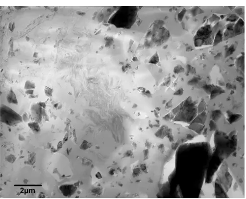
[image:10.612.46.297.486.689.2]Figure 1. Low resolution transmission electron micrographs of nanocompo-site materials showing the components having variable size and structure down to the nanometer level.
maximum (FWHM) and the degree of crystallinity can be ob-tained. The FWHM of the polyethylene crystalline peaks, i.e., FWHM (110) and FWHM (200), can be employed to describe the crystallization rate of HDPE/SiO2 nanocomposites.
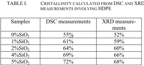
Table I shows the cristallinity as a function of load content obtained from the DSC and XRD measurements. It was found that as the content of nanocharges increased, the crystallinity of the nanocomposites also increased. A possible explanation is that the nanoparticles act as an agent of nucleation for the crys-tal growth.
B. Do chemical effects take over the nano-effects?
Dispersing nanoparticles into polymers lead to enhance-ment of thermal and mechanical properties of the composite with respect to the conventional material and it is hoped that similar effects could be observed on electrical performances. Improvement of electrical behaviour has indeed been reported on different types of PNC. Such modifications are attributed, besides to the presence of the filler, to the much higher surface area to volume ratio associated with the presence of nano-particles with respect to micrometric-size fillers. We would like to emphasize here that it is most of the time highly chal-lenging to relate changes of electrical properties with the nanometric size of the dispersion. This is so mainly because nano-particles dispersion into polymers involves complex preparation steps which can be highly influential on the elec-trical properties.
The case of one of the oldest polymer based nano-composite, layered silicate dispersed in polypropylene matrix, which has been characterized in details, is a perfect example. First, starting from isotactic polypropylene, a compatibiliza-tion process is needed since the matrix must be rendered polar to enhance PP chains entrance into clay galleries. To achieve this, maleïc anhydride (a polar species) is grafted on the PP chain using peroxide; this first step already involves several chemical by-products. The clay is also modified in terms of interlayer distance and organophilic capacity by exchange of intergallery sodium cations by protonated octadecylamine, a process that generates ionic moieties. This complex synthesis route [1] allows controlling the interactions between the host material and nanograins.
What is generally observed is that the PNC properties are different from those of the polymer alone [2, 3]. However, taking into account the complexity of the PNC, it becomes a difficult task to assign a given property evolution to a nano-size effect. All the involved chemical processes are not neutral when dealing with optical and electrical properties of the PNC. For example, it has been shown [3] that the optical properties in silicate PP based NC are mainly controlled by the compati-bilization process of the PP matrix and that the active recom-bination centers are those of the matrix. Space charge behav-iour has been shown to depend more on the matrix (isotactic vs. syndiotactic PP) than on the clay concentration. The di-electric losses are increased by the grafting and the clay con-centration and this is linked with the ionic species resulting from the manufacturing processes [4].
It is well established that dielectric properties and charge transport is highly sensitive to chemical/physical features of the matrix. Keeping in mind the example of PP based silicate NC, compatibilization and silicates dispersion change both the microstructure of the NC and its chemical nature. Through microstructure, the distribution of energy levels assisting elec-tronic charge transport is changed. Through chemistry, the density and depth of deep trapping centers giving rise to space charge phenomenon are also altered. The presence of ions would also change the electric and dielectric behaviour. This is to say that the attribution of a change in electrical properties to increase of the surface area to volume ratio should be done on the basis of experiments where every step in the preparation of the NCP is under control. This is very demanding from the point of view of material preparation but we believe it is the only way to go forward in the understanding of a specific ef-fect of the increased surface area to volume ratio.
[1] P. Reichert, H. Nitz, S. Klinke, R. Brandsch, R. Thomann, R. Multhaupt, “Polypropylene/organoclay nanocomposite formation: influence of com-patibilizer functionality and organoclay modification”, Macromol. Ma-ter. Eng. Vol. 275, pp. 8-17, 2000.
[2] G.C. Montanari, D. Fabiani, F. Palmieri, DK Kaempfer, R. Thomann, R. Multhaupt, “Modification of electrical properties and performance of EVA and PP insulation through nanostructure by organophilic silicates”, IEEE TDEI 11 5 pp. 754-762, 2004.
[3] M. Ambid, D. Mary, G. Teyssedre, C. Laurent, G.C. Montanari, "Optical properties and luminescence behaviour of PP/clay nanocomposites", Trans. Institute of Electrical Engineers of Japan, Vol. 126A, N°11, pp.1-8, 2006.
0 10 20 30 40 50 60 70 80
12 17 22 27 32 37 42 47 2θ (degree)
Re
la
ti
ve
in
te
n
sit
y
(a
.u
.)
Intensity 0 (%) Intensity 1 (%) Intensity 2 (%) Intensity 4 (%) Intensity 5 (%) ( 110)
Amorphous
( 200) FWHM
(a)
Figure 1. XRD patterns of HDPE/SiO2; Intensity versus angle diffraction for
0%, 1%, 2%, 4% and 5% nano-SiO2.
Samples DSC measurements XRD
measure-ments
0%SiO2 55% 52%
1%SiO2 61% 59%
2%SiO2 64% 60%
4%SiO2 69% 66%
5%SiO2 72% 68%
TABLE I. CRISTALLINITY CALCULATED FROM DSC AND XRD
[image:11.612.50.280.405.511.2][4] N. Fuse, T. Tanaka, Y. Ohki, “Evaluation of dielectric properties in polypropylene/clay nanocomposites”, CEIDP 2009.
C. Blurrs of the nano-effect in presence of inorganic oxide
nanoparticles in a polymers
The first successful nanocomposites incorporated nanoscale clay into a polymer host material [1]. The subsequent handling of these composites is well understood but the dielectric prop-erties are difficult to predict, due to the chemistry involved in introducing the clay into the polymer. An alternative to clay are nanoscale inorganic oxides, of which there is a wide range to choose from. Examples are Aluminum oxide (Al2O3),
alumi-num nitride (AlN), boron nitride (BN), magnesium oxide (MgO), silicon dioxide (SiO2) or titanium dioxide (TiO2) to
name a few. At the zeta potential where their agglomerates become unstable [2], these particles can be dispersed in a solu-tion by means of e.g. ultrasonificasolu-tion and consequently modi-fied with silane coupling agents (SCA) in order to keep them separated [3]. The SCA consists of a hydrolyzable and an or-ganofunctional group, which needs to be chosen according to the used host and filler material. Via the SCA the nanoparticles connect with the polymer host, forming strong bonds. It is agreed upon that the interfacial region between particle and host affects the dielectric properties [4, 5]. However, the exact nature of this interface region is still unclear.
Initial results regarding the permittivity of polymer-based nanocomposites were astounding since they defied conven-tional wisdom. Introducing a small fraction of nanoscale filler material into a polymer host reduces the relative permittivity. Traditional theories would suggest that a composite of two ma-terials would have a relative permittivity with a value between the values of the constituent elements, instead of being lower than either of them. The reason for this unique behaviour turned out to be an immobilization of polymer chains surround-ing the nanoparticles. This effect might very well occur in composites with conventional filler material, which is in the micrometer range, but was not perceived as a pivotal point for dielectrics. Due to the increased importance of the interfaces in nanodielectrics, this effect is of great importance. It leads to an important question: to what extent does the filler material in-fluence our composites? The previously often ignored struc-tural changes on a molecular level are now of high importance, as the aforementioned example illustrates.
The main parameters affecting the properties of a nano-composite can be identified as follows:
Filler size, material and aspect ratio
Surface functionalization
Fillgrade
Host material
Type of synthesis (in-situ, ex-situ, mixing process, po-lymerization, etc.)
These parameters consequently are reflected in the quality of dispersion of particles within the host material. Until re-cently the tendency was to assume that the host material does not change due to the introduction of fillers. Now we think that this is not the case and the presence of a filler material does
change the host itself. Polymer chains usually align according to intermolecular forces. The chains that bond to a particle sur-face via SCA are therefore forced to align according to their neighboring molecules. This leads to a restructuring of the host material due to the presence of the particle and its ability to interact with the host material. Question is now if the presence of the particle and its shape or aspect ratio is more significant than the material the respective particle consists of?
Looking at dielectric spectroscopy results on nanocompo-sites we notice a trend for the permittivity depending on the filler fraction. The real part of the permittivity is decreasing with decreasing nanoscale filler content, until it reaches a minimum which usually lies at filler contents lower than 2 % by weight or 0.35 % by volume [6, 7]. After this local mini-mum the permittivity increases, surpassing the value for the base material eventually. Here the properties of the filler mate-rial become more dominant compared to the changes in the host material. Where this point lies seems to be dependent on the particle properties (material, surface modification, size and fill grade). It is safe to say that none of the aforementioned in-fluences alone leads to the property changes. It is the combina-tion of all these factors that lead to the results and it is impor-tant for engineers dealing with nanocomposites to be aware.
The aspect ratio of the filler material is also of concern. Spherical particles lead to different properties than platelets or rods. Alignment of the filler within the matrix could also lead to differing results. If the filler distribution is random or if it is aligned to form chains throughout the composite, anisotropic behaviour may be the result. Future applications can exploit this anisotropy in various ways.
[1] A. Okada, Y. Fukushima, M. Kawasumi, S. Inagaki, A. Usuki, S. Sugiyama, T. Kurauchi, and O. Kamigaito, “Composite material and process for manufacturing same”, US patent no. 4.739.007, 1988 [2] M.J. Cromp, D.A. Oppermann, and K. Krehbiel, “Suspension properties
of hexagonal BN powders: effect of pH and oxygen content”, Journal of Materials Science, vol. 34, pp. 2621-2625, 1999.
[3] R. Kochetov, T. Andritsch, U. Lafont, P.H.F. Morshuis, and J.J. Smit, “Thermal Conductivity of Nano-filled Epoxy Systems”, Conference on electrical insulation and dielectric phenomena, Virginia Beach, VA, October 2009
[4] S. Rätzke, “Zur Wirkungsweise von nanoskaligen Füllstoffpartikeln in polymeren Isolierwerkstoffen der Hochspannungstechnik”, VDI Fortschritt-Bericht, Reihe 21, Nr. 387, VDI Verlag 2009
[5] T. Tanaka, M. Kozako, N. Fuse, and Y. Ohki, “Proposal of a Multi-core Model for Polymer Nanocomposite Dielectrics”, IEEE Transactions on Dielectrics and Electrical Insulation, Vol. 12, No. 4, pp. 669-681, 2005 [6] T. Andritsch, R. Kochetov, P.H.F. Morshuis, and J.J. Smit, “Dielectric
Properties and Space Charge Behavior of MgO-Epoxy Nanocomposites”, unpublished
[7] S. Singha, and M. Joy Thomas, “Reduction of Permittivity in Epoxy Nanocomposites at Low Nano-filler Loadings”, Conference on electrical insulation and dielectric phenomena, Quebec City, pp. 726-729, October 2009
D. Glass transition phenomenology
1) The nature of the glass transition.
amorphous linear polymers, for example, the glass transition corresponds to a change in modulus of several orders of mag-nitude, from a brittle solid well below the so-called glass tran-sition temperature (Tg) to a viscoelastic solid or viscous liquid
at higher temperatures. However, if mechanical properties are measured under an oscillatory strain, then the resultant marked decrease in modulus described above is seen to occur at a tem-perature that is dependent upon frequency; a lightly cross-linked rubber may appear elastomeric at 1 Hz but behave as a glassy solid at ultrasonic frequencies. If isochronal measure-ments of sample volume are made at constant pressure, the glass transition manifests itself as a change in the gradient of a plot of specific volume against temperature. The temperature at which this occurs is, however, dependent upon the length of time at which the specimen is held at each temperature prior to measuring its volume; the longer the time, the lower the ap-parent Tg.
The physical state of a glass is dependent upon many fac-tors, but it is rarely if ever, in thermodynamic equilibrium. For example, if a polymer is quenched from a temperature T1
to another temperature T2, where T1 > Tg > T2, then the initial
glassy state will depend upon both T1 and T2; thereafter, it will
tend to relax towards thermodynamic equilibrium, a process termed physical ageing. The origin of such effects is well il-lustrated by the Gibbs-DiMarzio theory, which builds on Flory’s earlier work on polymer solutions. Put simply, this envisages a polymer molecule as an array of contiguous cells within a lattice; adding more polymer molecules to the lattice increases the number of occupied cells and reduces the number and sizes of the “holes” between the polymer molecules (that is, the number of unoccupied lattice sites or the free volume of the system decreases). While the above has been stated in terms of adding more molecules to the lattice, equivalent proc-esses occur when a polymer is cooled. At some temperature, the distribution of free volume in the system is such that mo-lecular motion is no longer possible within the time scale of the measurement; free volume is envisaged as being dynami-cally created and destroyed lodynami-cally through the cooperative motion of chain segments. Although theory predicts a finite non-zero temperature at which the configurational entropy becomes zero, which would correspond to the thermodynamic
Tg, practically, the concept of Tg is best viewed in terms of free
volume and molecular mobility. As such, it is dependent upon molar mass, crosslinking, additives, interfaces, etc. For further details on the nature of the glass transition, reference to the excellent overview of McKenna [1] is recommended.
2) The glass transition in nanocomposites.
A key feature in the topic of nanocomposites concerns the role of interfaces and, as such, this area has received consider-able attention. In his 2004 paper, Lewis [2] considers the frac-tion of material adjacent to an interface within a nanocompo-site and points out that, in the case of an interphase region of thickness 10 nm, this component will dominate for particles less than about 100 nm in diameter. Numerous studies of nanocomposite interfaces have therefore been undertaken. For example, the application of X-ray photoelectron spectroscopy to PMMA/kaolinite [3] revealed an increase of 0.6 eV in the energy of the oxygen 1s orbital, which was ascribed to hydro-gen bonding between the carbonyl groups of the polymer and hydroxyl group in the kaolinite sheets. Electron spin resonance
studies of poly(methyl acrylate) (PMA) and synthetic fluoro-mica demonstrated that, in exfoliated systems, the local mobil-ity of PMA chains is reduced due to the interactions with the nanofiller. The thickness of the rigid interface region was es-timated to be in the range 5-15 nm [4].
Interactions such as those described above can have a marked influence on material confined near an interface and this is well illustrated by considering the case of ultrathin polymer films, where both the film thickness and specific in-teractions with any substrate can affect the glass transition.
Most results indicate that thickness effects begin to manifest themselves in the range 50–80 nm [5]; in the case of free standing ultrathin films of polystyrene, a large and molar mass dependent decreases in Tg has been observed [6]. In contrast,
in the case of poly(methyl methacrylate), much smaller effects have been reported [7] while, for poly(vinyl acetate), no change was seen [8]; in extremely thin films, the disappear-ance of a glass transition has been reported [9]. Such effects are generally attributed to reduced restrictions on molecular mobility with decreasing thickness. Where the film is sup-ported upon a substrate smaller decreases and even increases in Tg have been reported [9, 10]. Evidently, both geometric
and interaction effects are important.
Another area that has attracted considerable attention con-cerns the behaviour of confinement within pores. In the case of the small molecular system ortho-terphenyl (o-TP), a de-crease in Tg has been reported with decreasing pore size [11]
as a result of the material in the nanopores being constrained and vitrifying under conditions of constant volume (isochoric conditions); modelling of such systems [12] indicates that this is an intrinsic size effect related to the influence of a negative hydrostatic pressure on glass formation. Replacing the o-TP with a solution of polystyrene in the same solvent has been shown to result in a more complex form of behaviour involv-ing two glass transitions [13], one below and one above the Tg
measured for the equivalent bulk system. The lower of these, which decreases with decreasing pore size, relates to the phe-nomenon described above, while the higher is associated with molecular interactions at the pore surface. A more complex three layer model has also been proposed, based upon dielec-tric studies of the dynamic properties of low molar mass hy-drogen-bonded organic small molecules within porous sol–gel glasses [14]. Dielectric studies of propylene glycol and two poly(propylene glycol)s (PPGs) of different molecular weight confined in controlled pore glasses [15] have revealed a retar-dation and broadening of the α relaxation process associated with Tg, and the existence of an additional relaxation attributed
to the interaction of a few layers (hydrogen bonding effect) of the confined liquid with the surface of the pore. Elsewhere, Tg
has been found to vary in a non-monotonic manner [16], where Tg first decreases and then increases as the pore size is
![Figure 2. Breakdown strength vs. aging time for PNC with 0, 2 and 4 wt% synthetic organoclay [21]](https://thumb-us.123doks.com/thumbv2/123dok_us/1608611.113805/7.612.44.261.60.225/figure-breakdown-strength-aging-time-pnc-synthetic-organoclay.webp)
![Figure 3. AC erosion depth vs. voltage application time for PNC with 0, 2 and 6 wt% C15A [22]](https://thumb-us.123doks.com/thumbv2/123dok_us/1608611.113805/8.612.64.299.432.668/figure-ac-erosion-depth-voltage-application-time-pnc.webp)
![Figure 1. Real (a) and imaginary (b) part of the complex permittivity of ep-oxy/SiCp – 50 m composite as function of frequency (from [7])](https://thumb-us.123doks.com/thumbv2/123dok_us/1608611.113805/15.612.326.527.342.685/figure-real-imaginary-complex-permittivity-composite-function-frequency.webp)