City, University of London Institutional Repository
Citation
:
Themistos, C., Kalli, K., Komodromos, M., Markides, C., Quadir, A., Rahman, B. M. & Grattan, K. T. V. (2012). Low-loss multimode interference couplers for terahertz waves. Proceedings of SPIE, 8426, doi: 10.1117/12.925655This is the accepted version of the paper.
This version of the publication may differ from the final published
version.
Permanent repository link:
http://openaccess.city.ac.uk/12231/Link to published version
:
http://dx.doi.org/10.1117/12.925655Copyright and reuse:
City Research Online aims to make research
outputs of City, University of London available to a wider audience.
Copyright and Moral Rights remain with the author(s) and/or copyright
holders. URLs from City Research Online may be freely distributed and
linked to.
Low-loss multimode interference couplers for terahertz waves
Christos Themistos*
a, Kyriacos Kalli
b, Michael Komodromos
a, Christos Markides
a, Anita Quadir
c,
B. M. Azizur Rahman
c, Kenneth T. V. Grattan
ca
Frederick University, 7, Y. Frederickou Str., 1036 Nicosia, Cyprus;
bCyprus University of
Technology, 30 Archbishop Kyprianos Str. 3036 Lemesos, Cyprus;
cSchool of Engineering and
Mathematical Sciences, City University London, Northampton Square, EC1 0HB London, UK
ABSTRACT
The terahertz (THz) frequency region of the electromagnetic spectrum is located between the traditional microwave spectrum and the optical frequencies, and offers a significant scientific and technological potential in many fields, such as in sensing, in imaging and in spectroscopy. Waveguiding in this intermediate spectral region is a major challenge. Amongst the various THz waveguides suggested, metal-clad plasmonic waveguides and specifically hollow core structures, coated with insulating material are the most promising low-loss waveguides used in both active and passive devices. Optical power splitters are important components in the design of optoelectronic systems and optical communication networks such as Mach-Zehnder Interferometric switches, polarization splitter and polarization scramblers. Several designs for the implementation of the 3dB power splitters have been proposed in the past, such as the directional coupler-based approach, the Y-junction-based devices and the MMI-based approach. In the present paper a novel MMI-based 3dB THz wave splitter is implemented using Gold/polystyrene (PS) coated hollow glass rectangular waveguides. The H-field FEM based full-vector formulation is used here to calculate the complex propagation characteristics of the waveguide structure and the finite element beam propagation method (FE-BPM) and finite difference time domain (FDTD) approach to demonstrate the performance of the proposed 3dB splitter.
Keywords: Finite-element method (FEM), finite-difference time-domain method (FDTD), multimode interference (MMI) devices, terahertz (THz) waveguides, metal-clad dielectric-coated hollow glass rectangular waveguides.
1.
INTRODUCTION
In recent years extensive research has been carried out in the terahertz portion of the electromagnetic spectrum, which is loosely defined as the frequencies from 0.3 THz to 10 THz (wavelengths from 30 μm to 1,000 μm). Traditionally Terahertz science and technology has been applied in space spectroscopy, examining far-infrared radiation, molecular spectroscopy and in the diagnostics of plasma. Recent progress has witnessed a remarkable expansion of Terahertz technology to a wide range of components, instruments and applications1. These advances in Terahertz applications
depend on the transmission properties of Terahertz sources, the penetration of Terahertz radiation through dielectric materials and the high sensitivity of Terahertz sensors. Due to the absorption of THz radiation of dielectrics and metals, extensive research has been carried out in the development of efficient waveguide structures with minimal transmission losses as low as 1dB/m and minimal dispersion. Several waveguide designs have been proposed, including photonic crystal fibres, dielectric-lined2 and cylindrical hollow waveguides3 with dielectric coating4, on-chip terahertz circuits,
metallic slit, and microstrip circuits5.
Multimode interference (MMI) couplers have been widely used in the design of optoelectronic systems and optical communication networks, as well as building blocks for cascaded integration6. The unique characteristics of MMI
coupler devices make them an attractive choice for several wavelength-division multiplexing (WDM) systems.
MMI devices have been used to replace directional couplers due to the ease of fabrication, their advantages of compactness, large fabrication tolerance, wide bandwidth, excellent splitting ratio, as well as low-loss and polarization independence. The properties of MMI coupler devices are based on the self-imaging principle, where the input field profile is reproduced at periodic intervals7. These properties spawned a wide range of applications for WDM systems
using MMI devices. Among a few are power splitters8, arrayed waveguide filters (AWG)9, MMI-AWG-based
multiwavelength lasers10 and Mach-Zehnder Interferometric switches11.
2.
THEORY
The principle of self-imaging in MMI devices in which guided modes of a multimode waveguide (typically ≥ 3) are excited and interfere constructively to reproduce single or multiple images of the input field is central to the waveguide design. Selective excitation of the modes in an MMI structure and consequently the position of the images in the direction of propagation are subject to a set of self-imaging mechanisms7. Under the self-imaging mechanism the
periodicity of single or multiple images is based on a set of interference mechanisms. The effects of the width and the in the input field can yield to 1 × N or N × M beam splitters. The Symmetric Interference (SI) mechanism is the result of combining the even (symmetric) modes. Based on the SI mechanism single images of the input field launched inside the waveguide can be obtained at a self image length, Li, defined by:
)
(
4
3
4
3
1 0β
β
π
π−
=
=
L
L
i (1)where,
L
πis the is the coupling length and β0 and β1, the propagation constant of the fundamental and the first higherorder mode.
Earlier work12 on the General (GI) and Restrictive (RI) interference mechanisms has shown that the power loss, and the
loss imbalance of an MMI-based 3dB splitter is depended on the width and the wavelength variation. Furthermore the effects of the fabrication parameters and a comparison of the SI, GI and RI have been presented elsewhere13. In this
paper a detailed study of a novel MMI-based 3dB THz wave splitter implemented using Gold/polystyrene (PS) coated hollow glass rectangular waveguides and is presented, including the performance and the effects of the SI scheme.
3.
NUMERICAL ANALYSIS
The Finite Element method has emerged as one of the most powerful and successful numerical methods. A wide range of devices can be modeled from the formulations used in the FEM. The FEM offers accurate, versatile and flexible numerical analysis of optical waveguides14 and structures with arbitrary shapes, index profiles and anisotropies. In the
present study a full vectorial H-field formulation utilizing the perturbation technique15 including a penalty function has
been successfully applied for the modal analysis of the waveguide structure in order to determine the propagation constants of the fundamental and the first higher order modes and to estimate the MMI coupling length given in (1). The full vectorial formulation, in terms of the nodal values of the full H-field vector, is based on the minimization of the of the following functional14
(
)
* 1(
)
(
) (
*)
2*
p
dx dy
dx dy
ε
ω
μ
−⎡
∇×
⋅
∇×
+
∇ ⋅
∇×
⎤
⎣
⎦
=
⋅
∫
∫
Η
Η
Η
Η
Η
Η
(2)where
ω
2is the eigenvalue andω
is the angular frequency of the wave, H is the full vectorial magnetic field, *(asterisk) is the complex conjugate and its transpose,ε
andμ
are the permittivity and permeability respectively, andp
is the dimensionless penalty function16.The Beam Propagation Method is considered one of the most popular numerical analysis techniques for the design and modeling of optical devices. The Finite-Element Beam Propagation method17 (FE-BPM) is a full-vectorial method based
on the Crank-Nickolson scheme using Perfectly Matched Layer18 (PML) as absorbing boundary conditions (ABCs) to
truncate the computational domain. The FEM is applied to the BPM for the discretization of the computational domain, thus providing an effective numerical tool. The FE-BPM permits the propagation of an initial field and simulates the electromagnetic wave propagation. The FE-BPM has been used in the present work to obtain information regarding the optical properties calculated for any transverse cross section of the structure at any position along the axial direction. The Finite Difference Time Domain method (FDTD) has been regarded as versatile, useful and widely used electromagnetic tool. The performance of the FDTD is embellished with the development of new algorithms to cope with a wide variety of EM problems as well as ABCs19. The 2D FDTD has been widely used as a highly efficient method for
field using the coupled form of Maxwell’s equations. The Yee algorithm requires an upper bound on the time step
Δ
t
for numerical stability. The Courant-Friedrich-Levy (CFL) stability condition for the two-dimensional formulation is given by2 2
1
1
S c
t
x
y
= ⋅ Δ
+
Δ
Δ
(3)where
S
<
1
and c is the wave propagation speed for the two-dimensional FDTD case. The stability factor ensures its robustness when applied to a wider range of electromagnetic problems. In simulating the MMI device using the 2D FDTD method PML ABCs are applied to terminate the problem space and simulate the structure in the time domain.4.
RESULTS
A hollow core rectangular metallic waveguide with silica cladding was considered as the waveguide structure of the MMI device, where the interior of the metal-cladding is coated with dielectric material to reduce the modal loss. The cross section of the structure is presented in Fig. 1(a), where the complex refractive indices of the gold metal layer and the silica cladding are 281.55 419.74+ jand1.96 0.0061+ j, respectively at an operating frequency of 2.5 THz. The refractive index of Polystyrene, which was used as the coating material, was taken to be 1.58 0.0036 + j at the same frequency. Further, a complex refractive index of 6
1.0 1 10+ × − j
has been taken into account for the air core, to take into consideration the loss at the above frequency.
(a) (b) Figure 1. (a) Cross section of the metallic hollow core polystyrene coated waveguide, (b) MMI device layout.
The MMI height, HMMI was considered to be 1 mm, to ensure single mode variation along in the vertical direction, and
the metal thickness, tm, to be 0.5 μm. The core width and the polystyrene thickness were varied to achieve optimum
MMI width and minimum loss, respectively. The symmetric interference scheme has been considered for the MMI device, as presented in the structure layout in Fig. 1(b), where the input field is launched at the centre of the structure along the x-axis, at half the MMI height, HMMI. According to the self-imaging principle, the self-image length, Li, under
the symmetric interference scheme, is located at a distance of 3Lπ 4 along the direction of propagation, and therefore the two images of the launched field (half-power splitting) are expected to be at a distance of half the self-image length and spaced by a distance equal to the half of the MMI width, WMMI, as it is also shown in Fig. 1(b).
Initially, an MMI width of 3 mm has been considered and from the effective index and attenuation constant of the fundamental TM mode (named as TM0) obtained with the variation of the polystyrene thickness (not presented here) a
minimum loss of about 3 dB/m has been achieved for a polystyrene thickness of 20 μm, and therefore, the above thickness has been used throughout this work. For a square structure with a side width of 1.8 mm the modal loss for a polystyrene thickness 15 μm was found to yield to a value of about 1.1 dB. It should be noted that for a circular structure composed of the same material (where Ag was used for the metal-layer) and a core radius of 1.8 mm, a transmission loss of about 1 dB/m has been reported2 and this value is found to be in fine agreement with the modal loss obtained in the
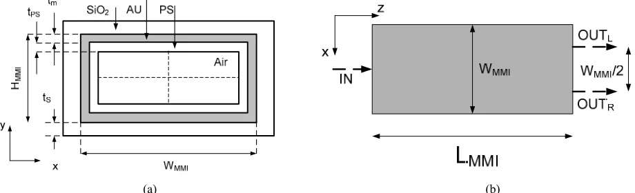
[image:4.612.82.542.333.473.2]Figure 2. Propagation characteristics of the fundamental, TM0 and the first higher order, TM1 mode, with the variation of the
MMI width, where he field profiles of the modes are shown as insets.
The propagation constant of the fundamental and the first higher order modes, named as TM0 and TM1, respectively,
with the variation of the MMI width, using the FEM, has then been examined. From the propagation characteristics, presented in Fig. 2, it can be seen that the propagation constants for the two modes increase with the increase of the polystyrene thickness. However, the propagation constant difference of the above decreases with the increase of the dielectric material thickness, thus giving rise to the coupling length of the device, according to (1) and consequently the length of the MMI.
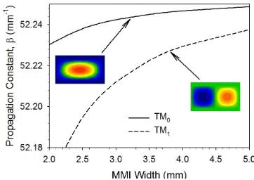
Figure 3. Half-power MMI length, LMMI and modal loss for the fundamental mode, with the variation of MMI width, WMMI.
The half-power MMI length, LMMI and the modal loss of the fundamental mode, for a polystyrene thickness of 20 μm
and an MMI height, WMMI, of 1mm, with the variation of the MMI width, has then been examined and presented in Fig.
3. As can be seen from the above characteristics the device length increases with the increase of the MMI width, while the attenuation decreases with the increase of the above dimension. As the MMI width increases above 3.0 mm the reduction of the loss starts converging to a value between 2.7 and 2.8 dB/m. The selection of the MMI width is a tradeoff of the device length and the attenuation. Therefore since the attenuation does not decrease significantly for an MMI width greater than 3 mm, the above dimension has been selected as the optimum width for the device examined. The propagation constants for the TM0 and the TM1 modes were calculated using the full vectorial H-field FEM and found to
be β0 = 52.2424 mm-1 and β1 = 52.2120 mm-1, respectively, thus giving a self image length, Li of 77.51 mm and
consequently a half power length corresponding to the length of the MMI of LMMI = 38.76 mm.
[image:5.612.205.406.328.456.2]0
1
2
3
0 5 10 15 20 25 30 35
x (mm)
z (mm)
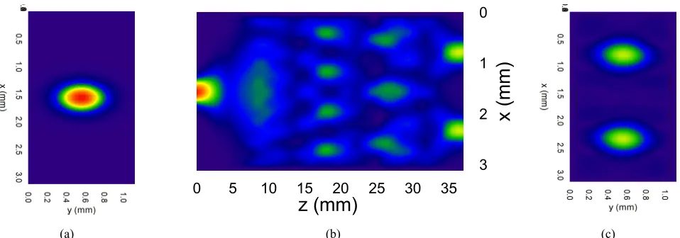
(a) (b) (c)
Figure 4. (a) Input Gaussian beam profile (b) H-field evolution along the direction of propagation and (c) profile of the
output half power images, from BPM simulation.
The two half-power images are formed at a device length, LMMI, between 37 and 39 mm, which is found to be in
agreement with the device length calculated using the FEM approach. It should be noted that it has been estimated (but not presented here) that the position of the maximum field intensity of the half-power images is dependent on the spot size diameter of the Gaussian beam. The optical field profiles obtained at the input and the output cross sections of the MMI device are also presented in Fig. 4(a) and Fig. 4(c), respectively.
Electric Field at 2.5 THz
0 0.005 0.01 0.015 0.02 0.025 0.03 0.035
-1.5 -1 -0.5 0 0.5 1 1.5
x 10-3
0 0.2 0.4 0.6 0.8 1
(a) (b)
Figure 5. (a) H-field evolution along the direction of propagation using FDTD and (b) output field at the left output port.
Further, the performance of the MMI device in the time domain has been examined using the FDTD approach. A Gaussian beam of spot-size diameter of 0.76 mm, launched the input of the MMI device has been simulated using the FDTD approach and the field evolution from a horizontal plane at the centre of the device, along the direction of propagation is presented in Fig. 5(a). The length of the device for the above spot-size diameter was found to be about 38.82 mm, in fine agreement with the length obtained from the FEM modal solution.Finally, the Electric field, obtained from the left port output of the MMI device, from the Gaussian input beam of spot size diameter of 0.76 mm, shown in Fig. 5(a), is presented in Fig. 5(b). The waveguide dispersion parameter, D, of the device at 2.5 THz was estimated to be about 0.1 ps/(μm-m). This corresponds to pulse broadening of about 0.85 ps for a 0.038 m long waveguide and a bandwidth of 1.4 THz. The dispersion level is also found to be in good agreement with the dispersion presented in previous work21 for a structure with circular geometry.
5.
CONCLUSION
[image:6.612.65.544.73.241.2] [image:6.612.63.541.333.482.2]1.1 dB/m and 0.1 ps/(μm-m), respectively and the reported transmission losses and dispersion levels of the waveguide structure are found to be in good agreement with previously published work.
REFERENCES
[1] P. H. Siegel, "Terahertz technology," Microwave Theory and Techniques, IEEE Transactions on, 50(3), 910-928 (2002).
[2] O. Mitrofanov, R. James, F. A. Fernandez et al., "Reducing Transmission Losses in Hollow THz Waveguides," Terahertz Science and Technology, IEEE Transactions on, 1(1), 124-132 (2011).
[3] C. Themistos, B. M. A. Rahman, M. Rajarajan et al., "Characterization of Silver/Polystyrene (PS)-Coated Hollow Glass Waveguides at THz Frequency," Lightwave Technology, Journal of, 25(9), 2456-2462 (2007). [4] B. M. A. Rahman, A. Quadir, H. Tanvir et al., "Characterization of Plasmonic Modes in a Low-Loss
Dielectric-Coated Hollow Core Rectangular Waveguide at Terahertz Frequency," Photonics Journal, IEEE, 3(6), 1054-1066 (2011).
[5] J. Cunningham, M. Byrne, P. Upadhya et al., "Terahertz evanescent field microscopy of dielectric materials using on-chip waveguides," Applied Physics Letters, 92(3), 032903-3 (2008).
[6] T. Trung Le, and L. W. Cahill, "The modeling of MMI structures for signal processing applications," Proc. SPIE, 6896, 68961G-7 (2008).
[7] L. B. Soldano, and E. C. M. Pennings, "Optical multi-mode interference devices based on self-imaging: principles and applications," Lightwave Technology, Journal of, 13(4), 615-627 (1995).
[8] T. Rasmussen, J. K. Rasmussen, and J. H. Povlsen, "Design and performance evaluation of 1-by-64 multimode interference power splitter for optical communications," Lightwave Technology, Journal of, 13(10), 2069-2074 (1995).
[9] M. R. Amersfoort, J. B. D. Soole, H. P. LeBlanc et al., "Passband broadening of integrated arrayed waveguide filters using multimode interference couplers," Electronics Letters, 32(5), 449 (1996).
[10] C. G. P. Herben, C. G. M. Vreeburg, X. J. M. Leijtens et al., "Chirping of an MMI-PHASAR demultiplexer for application in multiwavelength lasers," Photonics Technology Letters, IEEE, 9(8), 1116-1118 (1997).
[11] N. Yoshimoto, Y. Shibata, S. Oku et al., "High-input-power saturation properties of a polarization-insensitive semiconductor Mach-Zehnder interferometer gate switch for WDM applications," Photonics Technology Letters, IEEE, 10(4), 531-533 (1998).
[12] C. Themistos, M. Rajarajan, B. M. A. Rahman et al., "Rigorous Comparison of Parabolically Tapered and Conventional Multimode-Interference-Based 3-dB Power Splitters in InGaAsP/InP Waveguides," Appl. Opt.,
43(27), 5228-5235 (2004).
[13] C. Themistos, and B. M. A. Rahman, "Design issues of a multimode interference-based 3-dB splitter," Appl. Opt., 41(33), 7037-7044 (2002).
[14] B. Rahman, and J. Davies, "Finite-element solution of integrated optical waveguides," Lightwave Technology, Journal of, 2(5), 682-688 (1984).
[15] C. Themistos, B. M. A. Rahman, and K. T. V. Grattan, "Finite element analysis for lossy optical waveguides by using perturbation techniques," Photonics Technology Letters, IEEE, 6(4), 537-539 (1994).
[16] B. M. A. Rahman, and J. B. Davies, "Penalty Function Improvement of Waveguide Solution by Finite Elements," Microwave Theory and Techniques, IEEE Transactions on, 32(8), 922-928 (1984).
[17] S. Obayya, [Assessment of the Full-Vectorial Beam Propagation Method] John Wiley & Sons, Ltd, (2010). [18] J.-P. Berenger, "A perfectly matched layer for the absorption of electromagnetic waves," J. Comput. Phys.,
114(2), 185-200 (1994).
[19] A. Taflove, and S. C. Hagness, [Computational electrodynamics : the finite-difference time-domain method] Artech House, Boston, (2005).
[20] Y. Kane, "Numerical solution of initial boundary value problems involving maxwell's equations in isotropic media," Antennas and Propagation, IEEE Transactions on, 14(3), 302-307 (1966).