Leakage Read Fault in Nanoscale SRAM: Analysis, Test and Diagnosis
Luigi Dilillo
†Bashir M. Al-Hashimi
†Paul Rosinger
†Patrick Girard
†† † University of Southampton - Electronics and Computer Science (ECS) DepartmentMountbatten Building, Highfield, Southampton, SO17 1BJ, United Kingdom
††Laboratoire d’Informatique, de Robotique et de Microélectronique de Montpellier – LIRMM
161, rue Ada – 34392 Montpellier Cedex 5, France
Contact author Luigi DILILLO ld3@ecs.soton.ac.uk
Abstract
In this paper we study the impact of leakage currents on the operation of SRAM memories fabricated using nanoscale technologies. We show how the leakage currents, flowing through the pass transistors of unselected cells, may affect the read operation causing Leakage Read Faults (LRFs). The results of extensive Spice simulation on a 65nm SRAM are analyzed to evaluate the occurrence of the LRF for different operating conditions including supply voltage, temperature and frequency. Furthermore, the test requirements to cover LRFs are given and a low complexity (∼2N) March test is proposed for diagnostic purposes.
1.
Introduction
Embedded memories will continue to dominate future SoCs as predicted by the ITRS Roadmap that forecast for such devices a density of approximately 94% in ten years [1]. As a result, the SoCs yield will depend largely on memories and the development of efficient test solutions and repair schemes for memories will be essential.
Most of memory tests rely on classic fault models such as stuck at fault, coupling fault and transition fault. Although these fault models are still valid, there is a new class of faults, called dynamic, that is emerging in nanoscale memories. Such faults need complex patterns to be sensitized. Some works have been presented on this subject [2, 3] and they are mainly focused on test of dynamic faults caused by resistive defects. In this paper we focus on the faulty behavior of SRAM memories due to leakage currents in particular configurations. The presence of important leakage currents in deep submicron technologies (<90nm) is generally considered as a main concern especially in terms of power consumption and more recently in terms of fault modeling [4]. In SRAM memories, the leakage currents that flow through the two pass transistors of unselected cells interfere with the read operation. The read operation in SRAM memories relies on the detection of differential voltage level between the bit lines generated by the selected cell. In the same column
where the cell to be read is placed, leakage currents of unselected cells generate another differential effect that may be opposite to the one useful for the read function. The consequent “mask effect” is generally considered the cause of performance reduction in SRAM [4, 5], especially in terms of operating frequency reduction. In [5] the authors provide possible architectural modifications to compensate the leakage current on the bit lines. This methodology deals with the leakage problem, but it does it at expenses of an increased area overhead. In this paper we propose a detailed study on the read faults generated by leakage currents in SRAMs which do not employ the leakage compensation scheme proposed in [5], and propose a test procedure for covering these faults.
In this paper, we show how the mask effect due to leakage currents may induce the sense amplifier to be unable to detect properly the correct value for the memory output with the occurrence of Leakage Read Faults (LRFs). This theme, introduced in [6], is here treated in detail. In particular, the effect of the leakage currents on the read function is analyzed for various operating conditions in terms of supply voltage, temperature and frequency. This analysis is useful to evaluate the conditions that are most likely to present LRFs. We also formalize the requirements useful for the sensitization and observation of the LRF and we propose a low complexity (∼2N, where N is the number of cells) test for its coverage and diagnosis.
The rest of the paper is organized as follows. In Section 2, we describe the read operation in common SRAMs. In Section 3, we present the new fault model LRF, with the analysis for different conditions of voltage, temperature and frequency. The test approach is presented in Section 4. Conclusions and future work are given in Section 5.
2.
Background: SRAM read operation
In this section we describe the read operation in SRAM memories in order to explain the mechanism that involves Leakage Read Faults. In the SRAM memory array (see Figure 1), there is a pre-charge circuit (Pr) for each column, which is used to set the voltage level of the two
bit lines of the column (BL and BLB) at a fixed value - VDD for most SRAM memories. This action is necessary for a correct read operation.
Ci,0 Ci,1 Ci,2 Ci,3 Ci,4 Ci,5
WLi-1
WLi+1
BL0 BLB0 BL1 BLB1 BL2 BLB2BL3 BLB3 BL4 BLB4BL5 BLB
WLi
[image:2.595.53.287.126.238.2]Pr0 Pr1 Pr2 Pr3 Pr4 Pr5
Figure 1- A portion of an SRAM cell array with pre-charge circuits
When a read operation is acted on a certain cell, the pre-charge circuit is turned OFF on the two bit lines belonging to the cell. At this point, these bit lines are floating and charged to VDD and the read operation can start. Figure 2 shows a memory column with two cells, the pre-charge circuit and the sense amplifier. As an example, we perform a read operation on the top cell that stores a ‘1’. The read operation begins when the Word Line enable signal ( ) allows the connection of the cell with the two bit lines.
1 n WL −
Core-cell n-1
Pre-charge Circuit
PrecB WLn
Core-cell n
1
0
VDD VDD-∆BL
Sense Amplifier
1
0 1
1 00
BLB BL
Unselected cell
(cell not connected with BL and BLB) Selected cell
(cell connected with BL and BLB)
WL signal OFF WL signal on
WLn-1
Core-cell n-1
Pre-charge Circuit
PrecB WLn
Core-cell n
1
0
VDD VDD-∆BL
Sense Amplifier
1
0 1
1 00
BLB BL
Unselected cell
(cell not connected with BL and BLB) Selected cell
(cell connected with BL and BLB)
WL signal OFF WL signal on
WLn-1
Core-cell n-1
Pre-charge Circuit
PrecB WLn
Core-cell n
1
0
VDD VDD-∆BL
Sense Amplifier
1
0 1
1 00
BLB BL
Unselected cell
(cell not connected with BL and BLB) Selected cell
(cell connected with BL and BLB)
WL signal OFF WL signal on
WLn-1
Figure 2- Read operation in SRAMs
The cell stores a ‘1’, thus the left node is at ‘1’, i.e. VDD, while the right node is at ‘0’, i.e. 0V. During the read operation, the bit line on the left side remains at VDD because it is connected with the node of the cell at VDD, while the bit line on the right side, BLB, is connected with the node of the cell at ‘0’ and is partially discharged, reaching the voltage level VDD-∆BL. A sense amplifier detects this different voltage level (∆BL= VBL-VBLB) between the two bit lines and gives the output value, ‘1’. For a correct read operation ∆BL is about VDD/10 or
more. The read value would be ‘0’ in the opposite case when a cell storing a ‘0’ is selected, BL is partially
discharged at VDD-∆BL and BLB stays at VDD. The
above description shows that, for a correct read operation, the two bit lines connected to the selected cell need to be fully charged and equalized at VDD, otherwise erroneous values may be obtained during the read operation. In the next section, we show in detail how the leakage currents, significant in nanoscale technologies, can lead failing in the read operation of SRAMs.
3.
Leakage Read Fault
The read operation is based on the detection of ∆BL generated by the selected cell. Thus, any further voltage difference between the two bit lines and not generated by the selected cell may be the cause of an incorrect output value. Referring to Figure 2, we consider the cell storing a ‘0’, and placed in the lower position in the diagram. Although this cell is not selected for the read operation, it does interact with the bit lines BL and BLB, because of the leakage currents. In Figure 3, we show these interactions with some detail.
Tn3 Tn2
Tn1 Tp2
Tp1
S SB
Tn4 WLn= 0V
BLB BL
0 1
VDD VDD
UNSELECTED CELL
UNSELECTED CELL
Tn3 Tn2
Tn1 Tp2
Tp1
S SB
Tn4 WLn= 0V
BLB BL
0 1
VDD VDD
UNSELECTED CELL
UNSELECTED CELL
Tn3 Tn2
Tn1 Tp2
Tp1
S SB
Tn4 WLn= 0V
BLB BL
0 1
VDD VDD
UNSELECTED CELL
UNSELECTED CELL
Tn3 Tn2
Tn1 Tp2
Tp1
S SB
Tn4 WLn= 0V
BLB BL
0 1
VDD VDD
UNSELECTED CELL
[image:2.595.343.514.338.484.2]UNSELECTED CELL
Figure 3- Leakage currents through the pass transistors in an unselected cell
A typical SRAM cell has six transistors, organized as two inverters connected in a loop (Tn1+Tp1 and Tn2+Tp2) and two pass transistors (Tn3 and Tn4) that connect the cell with the two bit lines. When the cell is unselected, the Word Line selection signal is low (WLn=0) and the two pass transistors are OFF. Although the pass transistors are OFF, there is a certain amount of current that leaks through these two transistors discharging the bit lines. In particular, the leakage current that concerns transistor Tn3 has three components:
1. Subthreshold leakage current that flows from bit line BL, charged at VDD, to transistor Tn3 substrate that is polarised at 0V;
2. Gate leakage current that flows from bit line BL, charged at VDD, through the gate oxide, to the gate of transistor Tn3 that is at 0V (cell not selected). This current has been demonstrated to be significant for technologies <90nm [4].
[image:2.595.54.281.410.596.2]3. Junction leakage current that flows from bit line BL, charged at VDD, to node S of the cell that is at 0V. In nanoscale technologies the three components that compose the total leakage current are becoming more important with the reduction of the transistor size and the thickness of the gate oxide [7]. On the right side of the cell the leakage current that concerns transistor Tn4 has two components, i.e. the subthreshold and the gate leakage currents (1. and 2.), while the junction leakage current (3.) is not present because the cell node SB has the same voltage level (VSB=VDD) of bit line BLB.
The fact that the two nodes of the cell are at different logic levels has the consequence that in an unselected cell the leakage currents from the bit lines through the two pass transistors are not symmetric. In particular the leakage is higher on the side with the cell node at ‘0’, e.g. on the left side as in Figure 3. In practice, an SRAM memory column has hundreds of cells and only one cell at a time can be selected for the read operation. Each unselected cell of the column interacts with the bit lines BL and BLB, because of the leakage currents. The leakage currents drawn by each unselected cell affect the voltage difference observed by the sense amplifier.
1
1 0
0
0 1
1
1 0
0
0 1
0
0 1
0
0 1
0
0 1
0
0 1
1
1 0
S A VDD
VDD VDDVDD
Pre-charge
Selected cell
Unselected cells
BL BLB
1
1 0
0
0 1
1
1 0
0
0 1
0
0 1
0
0 1
0
0 1
0
0 1
1
1 0
S A VDD
VDD VDDVDD
Pre-charge
Selected cell
Unselected cells
BL BLB
1
1 0
0
0 1
1
1 0
0
0 1
0
0 1
0
0 1
0
0 1
0
0 1
1
1 0
S A VDD
VDD VDDVDD
Pre-charge
Selected cell
Unselected cells
[image:3.595.79.265.353.640.2]BL BLB
Figure 4 - The leakage effect in a memory column
Figure 4 shows a memory column where one cell, storing ‘1’, is selected for the read operation and the other cells are not selected and store various values. During the read operation, as explained in Section 2, the selected cell discharges partially one of the two bit lines and the sense amplifier detects the consequent voltage
difference and amplifies it for the output. In this case, the selected cell (on the top in Figure 4) partially discharges bit line BLB. Due to the leakage currents, also the unselected cells in the column give their contribution to the discharge of both bit lines BL and BLB in a different way, depending on the stored values. In particular, when the number of unselected cells storing a ‘0’ is higher than the number of unselected cells storing a ‘1’, the overall effect is that BL is more discharged than BLB. This effect of leakage currents is opposite to the effect of bit line discharge due to the r1 (read ‘1’) operation on the selected cell. In other words, the sum of the effects of the asymmetric leakage currents changes the voltage difference between the two bit lines. A significant reduction of ∆BL increases the noise sensibility of the device and may lead to faulty read operation. The importance of this mask effect is proportional to the number of cells storing ‘0’. At this point we can define the new fault model for SRAM memories as follows:
LRF: Leakage Read Fault – When in a memory column most cells store the same value X∈{0,1}, the leakage currents, through the pass transistors of the unselected cells may affect the read operation in the cells storing the value X , where X is the opposite of X: X is expected and X is read.
In order to identify the relation between the values stored in the cells of the column and the LRF occurrence, we have performed Spice simulation on a 1024x1024 SRAM memory using the 65nm Berkley Predictive Technology models [8], with a supply voltage of 0.7V, a temperature 125°C and a cycle time 3 ns. We have chosen to run the simulations at T= 125°C because at higher temperature the leakage currents increase. In these simulations, we consider the variation of the differential value ∆BL between the two bit lines, useful for the read operation, for different distribution of ‘0’ and ‘1’ in the cells of the column. The results of these simulations are given in Figures 5 and 6.
80 90 100 110 120 130 140 150 160 170 180
∆
BL
, m
V
50% ‘0’ &
50% ‘1’
40% ‘0’ &
60% ‘1’
30% ‘0’ &
70% ‘1’
20% ‘0’ &
80% ‘1’
10% ‘0’ &
90% ‘1’
1 ‘0’ & 102
3 ‘1 ’ 80
90 100 110 120 130 140 150 160 170 180
∆
BL
, m
V
50% ‘0’ &
50% ‘1’
40% ‘0’ &
60% ‘1’
30% ‘0’ &
70% ‘1’
20% ‘0’ &
80% ‘1’
10% ‘0’ &
90% ‘1’
1 ‘0’ & 102
3 ‘1 ’
50% ‘0’ &
50% ‘1’
40% ‘0’ &
60% ‘1’
30% ‘0’ &
70% ‘1’
20% ‘0’ &
80% ‘1’
10% ‘0’ &
90% ‘1’
1 ‘0’ & 102
3 ‘1 ’
Figure 5 – ∆BL reduction during the read operation, due to leakage currents
[image:3.595.315.521.562.716.2]The graph in Figure 5 shows the variation of the useful ∆BL in relation with the distribution of ‘0’ and ‘1’ stored in the column. The analysis of the graphs shows that the increase of the number of cells storing a ‘0’ reduces linearly the value of the useful ∆BL. We can identify two main situations:
- The average case is when in the column there are 50% of cells storing ‘0’ and 50% of cells storing ‘1’. In this configuration, the global leakage currents, through the cell pass transistors, are symmetric, thus they have no effect on the read operation: the useful ∆BL is the highest (160 mV).
- The worst case is when 1023 cells store a certain value, e.g. ‘0’, and only one stores the opposite value, ‘1’. During the reading of the cell storing a ‘1’, the leakage currents of all the unselected cells, storing a ‘0’,
contribute to reduce the ∆BL useful for the read
operation.
The graph in Figure 6, shows the percentage of reduction of the ∆BL, useful for the read operation, in relation with the average case (50% of cells storing ‘0’ and 50% of cells storing ‘1’) for different distributions of stored values.
0% 5% 10% 15% 20% 25% 30% 35% 40% 45% 50%
%
∆
BL
r
ed
u
ct
io
n
50%
‘0’ &
50%
‘1’
40%
‘0’ &
60%
‘1’
30%
‘0’ &
70%
‘1’
20%
‘0’ &
80%
‘1’
10%
‘0’ &
90%
‘1’
1 ‘0
’ & 1
023 ‘
1’
0% 5% 10% 15% 20% 25% 30% 35% 40% 45% 50%
%
∆
BL
r
ed
u
ct
io
n
50%
‘0’ &
50%
‘1’
40%
‘0’ &
60%
‘1’
30%
‘0’ &
70%
‘1’
20%
‘0’ &
80%
‘1’
10%
‘0’ &
90%
‘1’
1 ‘0
’ & 1
023 ‘
1’
50%
‘0’ &
50%
‘1’
40%
‘0’ &
60%
‘1’
30%
‘0’ &
70%
‘1’
20%
‘0’ &
80%
‘1’
10%
‘0’ &
90%
‘1’
1 ‘0
’ & 1
023 ‘
[image:4.595.313.548.221.394.2]1’
Figure 6 – %∆BL reduction during the read operation, due to leakage currents
In the worst case, there is a reduction of ∆BL of about 45%, in relation with the average case, with a value of
∆BL very close to safety value (VDD/10). The
consequence is that the memory in this condition is very sensitive to the noise and more prone to faults during the read operation. When ∆BL is close to the minimum safety value (VDD/10), any perturbation, such as VDD bounce, ground bounce and VDD droop, may potentially lead to a faulty read, i.e. an output value different from the expected one.
In the next three subsections, the results of further simulations are given to investigate the relevance of the
reduction of the read ∆BL with variation of important operational parameters.
3.1 Supply voltage analysis
Here, we consider the variation of the ∆BL, useful for the read operation, with the supply voltage. Figures 7 and 8 show the results of Spice simulations on the 65nm SRAM memory considered earlier, with supply voltage in the range from 0.5V to 0.8V, a temperature of 125°C and a cycle time of 3 ns.
0 50 100 150 200 250
0.50 V 0.55 V 0.60 V 0.65 V
0.70 V 0.75 V
0.80 V
0.00E+00 1.00E-06 2.00E-06 3.00E-06 4.00E-06 5.00E-06 6.00E-06 7.00E-06 8.00E-06 DBL Average Case, mV
'0' Leakage, A '1' Leakage, A
(a)
(b) (c)
0 50 100 150 200 250
0.50 V 0.55 V 0.60 V 0.65 V
0.70 V 0.75 V
0.80 V
0.00E+00 1.00E-06 2.00E-06 3.00E-06 4.00E-06 5.00E-06 6.00E-06 7.00E-06 8.00E-06 DBL Average Case, mV
'0' Leakage, A '1' Leakage, A
(a)
[image:4.595.52.290.376.532.2](b) (c)
Figure 7 – Average Case read DBL(=∆BL) and leakage currents through the pass transistors of unselected
cells in relation with VDD variation
In Figure 7, The curves at the top (a) and the bottom (b) are referred to the equivalent global (1023 cells at ‘0’, in the column) leakage currents (the scale is on the right, A) through the pass transistors on cell nodes at ‘0’, and through the pass transistors on cell nodes at ‘1’ respectively. The curve marked (c) shows the variation of ∆BL (the scale is on the left, mV) with supply voltage in the range from 0.5V to 0.8V. The analysis of curve (a) demonstrates that the intensity of leakage currents on the node at ‘0’ increases with the supply voltage, amplifying the mask effect on the read operation. Conversely, despite the larger leakage currents, the value of the useful ∆BL increases for higher supply voltage, see curve (c). The worst case is for lower values of VDD. In particular, for
VDD=0.5 the value of ∆BL is clearly inferior than
VDD/10. This unexpected result is due to the fact that the
augmentation of the read ∆BL is higher than the
augmentation of leakage currents. The consequent result is that for higher supply voltage the incidence of the LRFs is lower. This is also demonstrated by the graph in Figure 8 that gives the reduction percentage of read ∆BL for different VDD levels.
0% 20% 40% 60% 80% 100% 120%
0.50 V 0.55 V 0.60 V 0.65 V 0.70 V 0.75 V 0.80 V
%
∆
BL
r
ed
u
ct
io
n
Supply voltage 0%
20% 40% 60% 80% 100% 120%
0.50 V 0.55 V 0.60 V 0.65 V 0.70 V 0.75 V 0.80 V
%
∆
BL
r
ed
u
ct
io
n
0% 20% 40% 60% 80% 100% 120%
0.50 V 0.55 V 0.60 V 0.65 V 0.70 V 0.75 V 0.80 V
%
∆
BL
r
ed
u
ct
io
n
[image:5.595.62.296.82.211.2]Supply voltage
Figure 8 – %∆BL reduction, due to leakage currents, in relation with the supply voltage
The curve shows how the reduction of ∆BL is more
evident for lower supply voltage, regardless of the lower leakage currents.
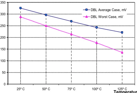
3.2 Temperature analysis
The variation of ∆BL with the temperature is considered here. The graphs in Figures 9 and 10 show the results of Spice simulations on the 65nm SRAM memory considered earlier, with supply a voltage of 0.8V, a temperature in the range from 25°C to 125°C and a cycle time of 3 ns.
0 50 100 150 200 250 300 350
25º C 50º C 75º C 100º C 125º C
DBL Average Case, mV DBL Worst Case, mV
Temperature
0 50 100 150 200 250 300 350
25º C 50º C 75º C 100º C 125º C
DBL Average Case, mV DBL Worst Case, mV
Temperature
Figure 9 – Average Case read DBL(=∆BL) and Worst Case DBL in relation with temperature variation
In Figure 9, the two curves show the variation of ∆BL in the Average Case and Worst Case, with the temperature in the range from 25°C to 125°C. The analysis of these two curves demonstrates that the read ∆BL decreases when the temperature increases. The influence of the leakage current in the reduction of the read ∆BL is more evident for higher temperature, because the distance between the two curves in the graph is larger for higher temperature. This result is more evident in the graph in Figure 10, which shows the reduction percentage of read ∆BL with the temperature: the reduction is more than linear.
0% 5% 10% 15% 20% 25% 30% 35% 40% 45%
25º C 50º C 75º C 100º C 125º C Temperature
%
∆
BL
r
e
d
u
c
ti
o
n
0% 5% 10% 15% 20% 25% 30% 35% 40% 45%
25º C 50º C 75º C 100º C 125º C 0%
5% 10% 15% 20% 25% 30% 35% 40% 45%
25º C 50º C 75º C 100º C 125º C Temperature
%
∆
BL
r
e
d
u
c
ti
o
[image:5.595.313.550.85.237.2]n
Figure 10 – %∆BL reduction, due to leakage currents, in relation with the temperature
3.3 Frequency analysis
In this subsection we study the variation of ∆BL, useful for the read function, in relation with the operation frequency. The graphs in Figures 11 and 12 show the results of Spice simulations on the 65nm SRAM memory considered earlier, with a supply voltage of 0.8V, a temperature of 125°C and a cycle time of in the range from 2ns to 3 ns.
The intensity of the leakage currents is independent to the frequency, because it is determined by technological parameters and other factors like supply voltage and temperature. This is confirmed by the graph in Figure 11 that shows that percentage of ∆BL reduction is almost constant in the observed range of frequencies.
0% 5% 10% 15% 20% 25% 30% 35% 40% 45% 50%
2ns 2.25ns 2.5ns 2.75ns 3ns
Cycle Time
%
∆
BL
r
ed
u
ct
io
n
0% 5% 10% 15% 20% 25% 30% 35% 40% 45% 50%
2ns 2.25ns 2.5ns 2.75ns 3ns
Cycle Time
%
∆
BL
r
ed
u
ct
io
n
0% 5% 10% 15% 20% 25% 30% 35% 40% 45% 50%
2ns 2.25ns 2.5ns 2.75ns 3ns
Cycle Time
%
∆
BL
r
ed
u
ct
io
n
Figure 11 – %∆BL reduction, due to leakage currents, in relation with the temperature
On the other hand, at higher frequencies the leakage currents have a larger impact on ∆BL reduction, because at higher frequency the read ∆BL is already reduced because the time useful to generate ∆BL is shorter. The further ∆BL reduction due to the leakage currents can be determinant for the manifestation of LRFs. This is confirmed by the graph in Figure 12, which shows that the
[image:5.595.56.293.407.569.2] [image:5.595.323.533.476.619.2]∆BL in the Worst Case is very close to 80mV=VDD/10 when the clock cycle of 2ns (highest simulated frequency).
0 50 100 150 200 250
2ns 2.25ns 2.5ns 2.75ns 3ns DBL Average Case, mV
DBL, Worst Case, mV
Cycle Time
0 50 100 150 200 250
2ns 2.25ns 2.5ns 2.75ns 3ns DBL Average Case, mV
DBL, Worst Case, mV
Cycle Time
0 50 100 150 200 250
2ns 2.25ns 2.5ns 2.75ns 3ns DBL Average Case, mV
DBL, Worst Case, mV
[image:6.595.76.258.120.243.2]Cycle Time
Figure 12 – Average Case read DBL(=∆BL) and Worst Case DBL(=∆BL) in relation with frequency variation
4.
Test and diagnosis
In sections 2 and 3, we have studied the configurations and conditions in which SRAM memories can be affected by LRFs. These configurations are summarized in the following three requirements:
a. In the column composed of m cells, m-1 cells have to store the same value X∈{0,1} and one cell has to store
X , where X is the opposite of X;
b. When the requirement a. is satisfied, a read operation is performed in the cell storing X (= Xr ).
c. The requirement a. and b. have to be verified for all the columns in the memory array and for both logic values. The first requirement (a.) is necessary for the sensitization of the LRF, while the second requirement (b.) is necessary for both sensitization and observation of the LRF. The third requirement (c.) is necessary because in nanoscale technologies there are often fluctuations of different parameters (e.g. Vth) even inside the die [9]. Thus, in the same memory array, there can be columns that present LRFs and fault free columns. Consequently, the test needs to be run in all the columns of the memory array.
The LRF is a dynamic fault because for its sensitization needs more than one operation (m+1). In the literature, there are different tests that meet the outlined three requirements. Among them, most known March tests are able to cover LRFs. However, these March tests generally target a large number of faults and consequently it can be difficult to use them for a diagnostic purpose. For this reason, we propose a March like test, named March LRF, which allows the test and diagnosis of LRFs. This test, depicted in Figure 13, is built on the test patterns that synthesize the three proposed requirements.
a a
-all a a
a -all
a
w0
;
r1
;
w0
w1
;
r0
w1
↑
c
↑
c
M0 M1 M2 M3
Figure 13 –March LRF: March like test for Leakage Read Faults
In order to make easier the understanding of March LRF, we perform its four elements in a hypothetical memory with 8 cells (N=8) and one column (n=1); one read/write operation is performed for each clock cycle. This process is shown in Figure 14.
Figure 14– Process of March LFR in an 8-cells memory
The element M0 operates a w1 in one cell of the column (Cell a) and w0 in all remaining cells (requirement a.). The element M1 operates the r1 ‘in cell a’ (requirement b.). The following two elements do the same operations inverting the written and read data (requirement c.). The complexity of this algorithm is 2N+2n (∼2N), where N is the number of cells and n is the number of columns in the memory. In order to make the March LRF more effective, it is possible to take in account the results discussed in Section 3. In particular, it would be useful to run the test in the conditions that maximize the presence of LRFs, i.e. low supply voltage, high temperature and the highest operating frequency.
5.
Conclusions
In this work we have introduced the new fault model Leakage Read Fault, which represents the mask effect of the leakage currents through the pass transistors of the unselected cells during the read operation in SRAM. The occurrence of the LRF depends on the distribution of the values stored in memory cells. We have evaluated the impact of this mask effect for different values of supply voltage, temperature and frequency. We have also studied the test approach by proposing three test requirements and a new March like test, named March LRF. This test has a low complexity (∼2N) and, targeting only the LFR fault model, is useful for diagnostic purpose. The authors intend to continue the present study concerning nanoscale SRAM by considering the interaction between the leakage mask effect that causes LRF and other sources of faulty read.#
Acknowledgments
L. Dilillo, P. Rosinger and B. M. Al-Hashimi acknowledge the Engineering and Physical Sciences Research Council (EPSRC) for funding this work under grant no. GR/S95770.
[image:6.595.309.545.149.274.2]References
[1] Semiconductor Industry Association (SIA), "International
Technology Roadmap for Semiconductors (ITRS)", 2003
[2] Z. Al-Ars and A.J. van de Goor, “Static and Dynamic
Behavior of Memory Cell Array Opens and Shorts in Embedded DRAMs”, Proc. Design, Automation and Test in Europe, 2001, pp. 496-503.
[3] L. Dilillo, P. Girard, S. Pravossoudovitch, A. Virazel, S.
Borri, M. Bastian, “Efficient March Test Procedure for Dynamic Read Destructive Fault Detection in SRAM Memories” Journal of Electronic Testing: Theory and Applications, Vol 21 N.5, 551-561, 2005, Springer Publisher
[4] S. Mukhopadhyay, H. Mahmoodi, K. Roy, “Modeling of
Failure Probability and Statistical Design of SRAM Array for Yeld Enhancement in Nanoscaled CMOS”, IEEE Trans. On CAD, vol. 24, NO.12, December 2005
.
[5] K. Agawa, H. Hara, T. Takayanagi, T. Kuroda, “A bitline
leakage compensation scheme for low-voltage SRAMs”, IEEE Journal of Solid-State Circuits, Volume 36, Issue 5, 2001, pp.726-734
[6] Ad.J.van de Goor, S. Hamdioui, R. Wadsworth, “Detecting
faults in the peripheral circuits and an evaluation of SRAM tests”, Proc. International Test Conference, 2004, pp.114-123
[7] Y. Taur and T. Ning, “Fundamentals of Modern VLSI
Devices”, Cambridge University Press, 1998
[8] UC Berkeley Device Group, “Berkeley Predictive
Technology Model”, Online, http://www.eas.asu.edu/~ptm/,
2005
[9] S. Borkar, T. Karmic, S. Narendra, J. Tschanz, A.
Keshavarzi and V. De, “Parameter variation and impact on circuits and microarchitecture”, in Proc. Design Automation Conference, 2003, pp. 338-342