The development of electrical plasma diagnostics for
HiPIMS discharges
Thesis submitted in accordance with the requirements of the University of Liverpool for the degree of Doctor in Philosophy
by
Phitsanu Poolcharuansin
Abstract
High power impulse magnetron sputtering (HiPIMS) is a plasma-based thin film de-position technique in which extremely high power pulses are applied to a conventional magnetron sputtering source. As a result, the plasma density in HiPIMS discharges is considerably increased up to 1019m−3, about three orders of magnitude higher than that in conventional direct current magnetron sputtering (DCMS) discharges. Hence the vapour of the sputtered species becomes highly ionised, leading to remarkable im-provement in the microstructure and the properties of depositing films.
To better control the deposition process, it is important to gain insights into the properties and the dynamics of the HiPIMS plasmas. This thesis is associated with the investigations on HiPIMS plasmas using a number of electrical diagnostic tools including a Langmuir probe, a retarding field energy analyser and a gridded quartz crystal microbalance.
Publications
“Short- and long-term plasma phenomena in a HiPIMS discharge” P. Poolcharuansin and J.W. Bradley
Plasma Sources Sci. Technol. 19 (2010) 025010
“Plasma parameters in a pre-ionized HIPIMS discharge operating at low pressure”
P. Poolcharuansin, B. Liebig, and J. Bradley
IEEE Trans. Plasma Sci. 38 (2010) 3007
“Time-resolved Langmuir probe measurements in preionised HiPIMS dis-charge”
P. Poolcharuansin, J.W. Bradley and P.J. Kelly
Materials Technology. 26(2011) 25
“The evolution of the IEDFs in a low-pressure HiPIMS discharge” P. Poolcharuansin, J.W. Bradley
Surf. Coat. Technol. 205 (2011) S307
“More evidence for azimuthal ion spin in HiPIMS discharges” P. Poolcharuansin, B. Liebig and J.W. Bradley
Plasma Sources Sci. Technol. 21 (2012) 015001
“Ionized metal flux fraction measurements in HiPIMS discharges” P Poolcharuansin, M Bowes, T J Petty, J W Bradley
J. Phys. D: Appl. Phys. 45(2012) 322001
“Low pressure HiPIMS operation using a pre-ionizer technique” P. Poolcharuansin and J.W. Bradley
53rd Conference proceedings of the society of vacuum coaters. (2010) 36
“Time-resolved ion energy distribution functions in a HiPIMS plasma using a retarding field analyzer”
P. Poolcharuansin, J.W. Bradley
54th Conference proceedings of the society of vacuum coaters. (2011) 166
“Azimthal ion spin in HiPIMS discharges” J.W. Bradley, P. Poolcharuansin and B. Liebig
Acknowledgement
This is an opportunity to say “thank you” to people who supported and guided me during my course in University of Liverpool.
I am very grateful to thank my supervisor Prof. James W Bradley for the advice and the help given to me over the years.
I would like to thank Dr Dmitry Samsonov, Dr Paul M Bryant and Dr James L Walsh for their useful comments and discussions.
I also wish to thank Mr Alan Edwards, Mr John Owens and Mr Alan Roby for their technical support in electrical and mechanical works.
Special thanks I would give to all my friends here in technological plasmas group for their nice friendship. Bernd Liebig for his informative comments and collaborations. Dr Jun-Seok Oh for daily discussions during our tea break time. Anurag Mishra for the training he has given during the beginning of the course. Michael Bowes and TJ for fruitful collaborations and their comments on my thesis writing.
Contents
Abstract i
Publications ii
Acknowledgement iii
Contents vi
List of Figures viii
List of Tables ix
1 Introduction 1
2 Literature review 3
2.1 Plasmas in general concepts . . . 3
2.1.1 Fundamental processes of non-thermal plasmas . . . 4
2.2 Sputtering . . . 5
2.3 Magnetron sputtering . . . 7
2.4 High power impulse magnetron sputtering . . . 8
2.4.1 HiPIMS discharge processes . . . 11
2.4.2 Plasma investigations . . . 14
2.5 Conclusions . . . 15
3 Plasmas diagnostics 16 3.1 Background . . . 16
3.2 Langmuir probe. . . 17
3.2.1 Principle . . . 17
3.2.2 Probe design . . . 18
3.2.3 Data analysis . . . 19
3.2.4 I-V Acquisition system . . . 22
3.3 Retarding field analyser . . . 23
3.3.1 Principle . . . 23
3.3.2 Modes of operation . . . 23
3.3.3 The probe requirements . . . 25
3.3.4 Probe design . . . 27
3.3.5 Data analysis . . . 28
3.4 Gridded quartz crystal microbalance . . . 30
3.4.1 Principle . . . 30
3.5 Summary . . . 34
4 Short and long term phenomena 35 4.1 Background . . . 35
4.2 Experimental arrangement. . . 36
4.2.1 The HiPIMS system . . . 36
4.3 Results and discussions . . . 39
4.3.1 Characteristic of the discharge . . . 39
4.3.2 Effect of operating pressure . . . 48
4.4 Conclusions . . . 51
5 Low-pressure operation technique 53 5.1 Background . . . 53
5.2 A HiPIMS system . . . 54
5.2.1 The vacuum station . . . 54
5.2.2 The magnetron source . . . 56
5.2.3 The power supply . . . 57
5.3 Delay times of current onset . . . 58
5.4 Pre-ionisation techniques. . . 59
5.5 Plasma characterisations . . . 62
5.5.1 Evolution of the plasma parameters . . . 63
5.5.2 IMS and IEDF . . . 66
5.6 Conclusions . . . 69
6 Ion velocity distribution functions 71 6.1 Background . . . 71
6.2 Experimental arrangement. . . 72
6.3 Optimisation of the RFA. . . 74
6.4 Validation of the RFA . . . 78
6.5 Time-resolved IEDFs . . . 81
6.6 Conclusions . . . 82
7 Azimuthal ion fluid motions 84 7.1 Background . . . 84
7.2 Experimental arrangement. . . 85
7.2.1 Operation of the HiPIMS discharge. . . 85
7.3 Results and discussions . . . 87
7.3.1 Spatial distributions of IEDFs . . . 87
7.3.2 A model of ion fluid rotation . . . 89
7.4 Conclusions . . . 95
8 Ionised metal flux fraction 96 8.1 Introduction. . . 96
8.2 Experimental arrangements . . . 97
8.3 Results and discussions . . . 98
8.4 Conclusions . . . 104
9 Conclusions and future work 105 9.1 Conclusions of the study . . . 105
Appendix 109
A Derivations 110
A.1 A brief of OML theory . . . 110
A.2 The estimation for Maxwellian electron density . . . 112
A.3 IVDF from the first derivative of an I-V curve . . . 113
A.4 The equations of circular motion . . . 114
A.4.1 Radial force: F~r. . . 115
A.4.2 Drag force: F~d . . . 115
B Gas oscillation 117
C List of symbols 121
List of Figures
2.1 DC diode sputtering system . . . 6
3.1 Electrical probe in a plasma . . . 17
3.2 Schematic diagram of the Langmuir probe . . . 18
3.3 A diagram of the probe biasing technique . . . 20
3.4 Ion current and electron current part in anI-V curve . . . 21
3.5 Voltage distribution inside RFAs . . . 24
3.6 Schematic diagram of the RFA . . . 25
3.7 Plasma penetration into the RFA . . . 26
3.8 Layout of the RFA . . . 27
3.9 I-V characteristic of the RFA . . . 29
3.10 Diagram of a g-QCM . . . 32
3.11 Deposition rate as a function of Pdis . . . 33
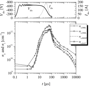
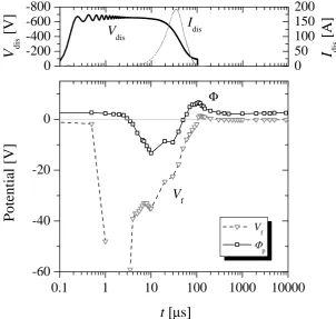
4.1 Experimental arrangement. . . 37
4.2 Abnormal I-V characteristics . . . 38
4.3 Waveform ofVdis and Idis . . . 39
4.4 Comparision of temporal neand ni . . . 40
4.5 Temporal ne,OML . . . 41
4.6 Temporal Vf and Φ . . . 43
4.7 Comparison of temporalVf . . . 44
4.8 Temporal Te . . . 45
4.9 The evolution of the EEDFs . . . 46
4.10 ne for super-thermal, hot and cold electrons . . . 47
4.11 Temporal ne for a number of pressures . . . 49
4.12 Temporal Vf and Φ for a number of pressures . . . 50
4.13 Temporal Te for a number of pressures . . . 51
5.1 Vacuum station . . . 55
5.2 Schematic diagram of the vacuum system . . . 55
5.3 Magnetic field mapping of the magnetron . . . 56
5.4 Block diagram of HiPIMS power supply . . . 57
5.5 Vdisand Idis waveforms. . . 57
5.6 Idis during a typical HiPIMS pulse . . . 59
5.7 Diagram of the pre-ionised HiPIMS power supply . . . 60
5.8 Vdisand Idis for a pre-ionised HiPIMS discharge . . . 60
5.9 Simple equivalent of HiPIMS circuit . . . 61
5.10 Temporal plasma parameters of the low pressure HiPIMS . . . 65
5.11 Temporal plasma parameters during off-time . . . 66
5.13 Mass/charge spectrum . . . 68
5.14 IEDFs of Ar+, Ti+, Ti2+ ions . . . . 69
6.1 Waveforms ofVdis and Idis . . . 73
6.2 The RFA arrangements . . . 74
6.3 Ic as a function ofVd . . . 75
6.4 Contour of Ic and dIc/dVd . . . 76
6.5 An IVDF plot. . . 77
6.6 Plots of ion parameters . . . 78
6.7 Time-resolved IVDFs. . . 79
6.8 IEDFs of main ionic species . . . 80
6.9 Comparison: Φ andVd at dIc/dVd peak . . . 80
6.10 Parameters comparison . . . 82
7.1 Experimental arrangement. . . 86
7.2 I-V curve and dIc/dVd of the RFA . . . 87
7.3 fi(ε) in contour plots . . . 88
7.4 hεii,hvii and Γi for different RFA positions . . . 89
7.5 fi(ε) ploted in contour manner . . . 90
7.6 Fϕ,Fr, Φpl and Er as a function of r . . . 92
7.7 The calculated trajectory of an ion fluid element . . . 94
7.8 Plots of calculateds,r,hvii . . . 94
8.1 Experimental arrangement. . . 98
8.2 The discharge waveforms for different parameters . . . 99
8.3 The deposition rate as a function ofVQ . . . 100
8.4 Depositions rates as a function ofPavg . . . 101
8.5 Corresponding flux as a function ofPavg . . . 102
A.1 A cross-section of a cylindrical probe . . . 110
A.2 A point Q in the polar coordinate . . . 114
B.1 Vdisand Idis waveforms for a long pulsed discharge . . . 118
List of Tables
4.1 The short-term and long-term decay times of the plasma parameters
obtained in the off-time for a number of different argon pressuresp and
peak discharge target densitiesPdis. . . 42
5.1 The reported process parameters and a number of relevant parameters
obtained from the discharge waveformsVdis,Idis and Pdis in figure 5.5. . 58
5.2 The selected process parameters for the plasma investigation. . . 63
6.1 Related parameters from IVDF . . . 77
7.1 A summary of the relevant parameters to calculate the average azimuthal
force per ion Fϕ in thex-y plane atz = 20 mm above the target surface. 91
8.1 Summary of pulse parameters used to power up the HiPIMS discharge
by adjustments of initial target voltageU0, pulse widthwand frequency
f. . . 98
B.1 The selected process parameters to observe the dynamics of long pulsed
Chapter 1
Introduction
Plasmas are ionised gases consisting of a large number of free charged particles, i.e. electrons and ions, in a volume of background neutral species. Unlike ordinary gases, plasma dynamics are dominated by long-range Coulomb interactions instead of short-range head-on collisions. In general, plasmas can be classified thermodynamically into thermal and non-thermal equilibrium states. In the latter case, which is often re-ferred to as technological plasmas, the average temperature of the electrons is about 100 times higher than the temperature of the ions and the neutral species (which are near a room-temperature). These energetic electrons can essentially provide a variety of low-temperature free-space active species, e.g. photons, radicals and ions that are advantageous to many technological applications. For example, photons in the ultra-violet energy range can be emitted from plasmas exciting the phosphor in fluorescent lamps and in flat-panel displays. Chemically active radicals in plasmas can sterilize biomedical tools, purify drinking water and clean up air pollution. Moreover, positive and negative ions generated from plasmas are crucial for instances in chemical etching during microelectronic fabrication and in physical vapour deposition during thin film material synthesis and engineering.
Ionised physical vapour deposition (IPVD) is a plasma-based thin film deposition technique in which the vapour of depositing material is dominated by ionic species rather than neutral particles [1]. Having high fluxes of the ionic species, IPVD po-tentially offers technological advantages over conventional physical vapour depositions. Firstly, depositing ions can be collimated by the plasma sheath resulting in anisotropic deposition for filling vias and trenches in micro-electronic fabrication. Secondly, bom-bardment by depositing ions can enhance the surface mobility of a depositing material leading to a denser microstructure and higher adhesion for tribological coatings. Fi-nally, the kinetic energy of depositing ions can be controlled by biasing the substrate, enabling one to adjust the properties of the deposited film.
sputtering operated in a pulsed mode in which low-frequency (50−1000 Hz), short-duration (0.5−20% duty cycle), high-power pulses (0.2−3.0 kWcm−2) are employed to increase the density of magnetised electrons up to 1019cm−3. As a result, the degree of ionisation of sputtered species is substantially increased. These plasma conditions give rise to considerable improvements to the micro-structure and properties of grow-ing films. The micro-structure of thin films deposited from HiPIMS processes are very dense, void-free structures, with low surface roughness and high adhesion. Conse-quently, film properties, for example the wear resistance coefficient of CrN, the hardness of TiN and the refractive index of TiO, are remarkably improved in comparison to that of the films grown in a conventional dc magnetron sputtering (dcMS) discharge.
In the last decade, HiPIMS is increasingly interesting not only in thin film indus-try but also in fundamental research. Many efforts have been made to gather basic parameters and to understand the physics of HiPIMS plasmas through experimental and theoretical works. Basic parameters of HiPIMS plasmas have been spatially and temporally measured using a variety of diagnostic tools. For example, temperature, density and energy distribution of electrons can be measured using Langmuir probes. The composition of the plasmas can be obtained using mass spectrometry or optical emission spectroscopy. The energy distribution of ionic species can be obtained by the use of energy analysers. The density of neutral species both in ground and metastable states can be determined from optical absorption spectroscopy. These basic param-eters of HiPIMS plasmas also reveal interesting regimes in the physical phenomena, for example, self-sustained sputtering, discharge runaway, strong gas rarefaction and cross-field azimuthal ion spin. Some of these phenomena in HiPIMS plasmas are not fully understood and need to be investigated in more details, which is the aim of this thesis.
The main propose of this thesis is to better understand physical phenomena in HiPIMS by plasma investigations using a number of plasma diagnostic tools including Langmuir probes, a retarding field analyser and a biased quartz crystal microbalance.
Chapter 2
Literature review
In this chapter, fundamental concepts underpinning HiPIMS plasmas are summarised. It includes general concepts and processes of plasmas and magnetron sputtering. Fur-ther comprehensive details of these concepts and processes are given in the textbooks of plasma processes and thin film deposition [3–6]. In the latter part of this chapter, the general perspective on HiPIMS plasmas is also given to point out issues that are relevant to this thesis.
2.1
Plasmas in general concepts
Plasmas have been recognized as the fourth state of matter in addition to solids, liquids and gases. Atoms in a solid have low kinetic energy, and are bound into a rigid structure by, for example an ionic bond. Breaking the bond using sufficient thermal energy, the state can be changed to liquid and then gas through melting and vaporisation, respectively. By supplying more thermal energy, gas atoms may be ionised, becoming free electrons and ions, due to collisions with energetic atoms. The state in which gases are ionised to become charged particles is referred to as the plasmas state.
The most fundamental characteristic of plasmas is its ability to neutralise the elec-trical charges. In other words, plasmas are quasi-neutral, i.e., charges in plasmas are conserved. For example, in singly charged plasmas, the electron density is approxi-mately equal to the density of singly charged ions. Any perturbation from external electric fields is shielded within a specific space and time. The length from the perturb-ing sources that plasmas can shield is determined by the Debye length,λDe. The time that plasmas can respond to shield is given by the inverse of plasma frequency,ωe. Both λDe and ωe depend on the fundamental parameters including electron temperatureTe and electron density ne. Other plasma parameters involved with space and time are often considered as a function of λDe and ωe, respectively.
con-stituent species, i.e., electrons, ions and neutrals, are nearly identical and much higher than room temperature. In technological applications, thermal plasmas are suitable for processes that require extremely high temperatures, e.g., plasma spraying, welding and cutting. Plasmas, on the other hand, can also be generated at lower temperature. In this case, electrons are heated, using external electric fields, to temperatures on the order of 105 K. Gas atoms can be ionised effectively during inelastic collisions with energetic electrons. In this way, the temperature of ions and neutrals remains at room temperature. These types of plasmas are known as non-thermal plasmas and are the subject of the thesis.
2.1.1 Fundamental processes of non-thermal plasmas
Gas state processes, both in the plasma bulk and at the boundary, are mainly involved with neutral particles. Unlike ordinary gases, non-thermal plasmas contain an amount of charged particles in addition to the residual neutral atoms. In the plasma bulk, col-lisions between charged particles and residual neutrals are of importance, in addition to collisions between neutrals. At the boundary, charged particles also interact with any surface that is adjacent to it. The collisions in the plasma bulk and interactions at the plasma boundary cause a number of subsequent processes that are vital in techno-logical applications. The important processes in non-thermal plasmas are summarised as follows.
Inelastic collisions between electrons and residual neutrals are one of the most important events in the plasma bulk. The kinetic energy of the electrons is effectively transferred to the neutrals causing a variety of collisions processes, e.g. dissociation, excitation, ionisation. As a result, radicals, excited species, photons and positive or negative ions can be generated. Those species generated in the plasma bulk are crucial and employed in a wide range of applications. For example, radicals such as ozone (O3), are utilised to purify water. Photons in a specific energy range are used in laser technology and lighting systems. Positive and negative ions are useful for surface engineering, by chemically and physically reacting with a surface.
Plasma sheaths accelerate ions from the plasma bulk to the walls with a particular kinetic energy depending on the potential different between the wall and the plasmas. If the wall potential is negative with respect to the plasma potential, positively charged ions are thus accelerated to the wall and may cause a number of processes which are described below.
Secondary electron emission: A solid surface, when bombarded by energetic
particles, can emit free electrons. Ions accelerated through a plasma sheath can be used as the energetic particles bombarding a surface in the vicinity of the plasma. The free electrons produced from a surface are crucial to generate and sustain non-thermal plasmas. These free electrons are often known as secondary electrons. Secondary electrons can effectively couple or absorb the energy from the electric field in the plasma sheath. When entering to plasma bulk, the secondary electron transfers its energy to other species via inelastic collisions. The number of secondary electrons produced by an incident ion is referred to as secondary electron emission yield,γse. Normally,γseis about 0.1 for metals.
Sputtering: If the kinetic energy of the bombarding ions is high enough, atoms
of the bombarded surface can be ejected out into a vapour. This process is known as sputtering. The vapour of sputtered atoms then diffuse from the target surface and condense as a thin film on other surfaces nearby. This is one of the established methods to deposit thin films. The details of sputtering as a thin film deposition tools are given in the next section.
2.2
Sputtering
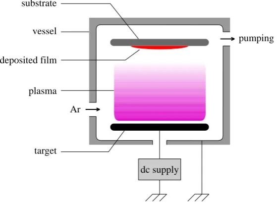
Sputtering is the physical process in which atoms are ejected from a surface due to bombardment by energetic particles. The energetic particles may be neutral particles or ions. In most cases, ions at the plasma boundary are used as sputtering particles due to them being accelerated towards a surface. In thin film technology, sputtering is categorised as a physical vapour deposition (PVD) technique. To understand the principles of sputtering processes for thin film deposition, a simple dc diode system is employed as shown in figure 2.1.
A dc diode sputtering system consists of a vacuum system, a sputter source, a negative dc power supply and a substrate. The vacuum system including the vessel, the pumps and the relevant vacuum devices is used to establish, monitor and control the operating pressure of the order of a few hundred mTorr. The diode sputter source is simply a metallic electrode used as a target in the sputtering process. The target is connected to a negative dc power supply, while the vessel is electrical grounded. A substrate, the object that is being deposited with the sputtered vapour, is placed several centimetres away from the target surface.
namely vapour generation, transportation and condensation. Initially, a plasma of an inert gas, commonly argon, is formed. The ions at the plasma boundary in the vicinity of the target are accelerated through a high voltage plasma sheath toward the target surface. The kinetic energy of the sputtering ions can be gained to the energy that corresponds to the target voltage which is normally in the range of several hundred volts. Atoms at the target surface are sputtered by momentum transfer and cascade collision mechanisms. The sputtered vapour then diffuses outward from the target surface toward the substrate. When the sputtered flux reaches the substrate surface, where the temperature is lower than the melting point of the target material, it condenses back to a solid state, forming a thin film over the substrate surface.
The main drawback of sputtering is the low rate of deposition compared with that from other PVD techniques, for example thermal and electron-beam evaporations. The rate of deposition for a given target material and a target voltage mainly depends on the density of the argon ions which relates directly to the density of the argon neutrals and the electrons in the system. Through increasing the number of argon neutrals in the chamber by increasing the operating pressure, the population of the positive argon ions in the plasma may be potentially increased. Nevertheless, numerous researches have shown that there is an optimum point for the operating pressure to achieve a high deposition rate. It means that the deposition rate will be reduced if the processes are operated at a pressure higher or lower than the critical pressure. Alternatively, increasing the electron density by plasma confinement near the target surface using external magnetic fields is the most effective means for increasing the density of argon ions. This strategy is one of the breakthroughs of sputtering technology and it is referred to as “magnetron sputtering”.
Ar
pumping
dc supply target
deposited film vessel substrate
[image:16.595.183.463.503.709.2]plasma
2.3
Magnetron sputtering
Magnetron sputtering is a magnetically enhanced sputtering technique in which an external magnetic field with a specific design is used to increase the plasma density, and hence deposition rate. Magnetron sputtering can operate with a higher deposition rate at a lower working pressure (1-5 mTorr) and a lower electric potential (300 – 700 V) in comparison with conventional sputtering [7]. Thornton has given the definition of the magnetron sputtering source in [8] as follows:
“Magnetron sputtering sources can be defined as diode devices in which magnetic fields are used in concert with the cathode surface to form electron traps which are so configured the E×B electron-drift currents can close on themselves.”
Over decades, various types of magnetron sputtering sources have been invented and investigated. Magnetron sources may be separated into three main categories using the criteria of target shape, magnetic configuration and driving power supply.
A sputtering target connected to a magnetron source may be presented in different geometries, including post, hollow cylinder, conical, hemispherical and planar mag-netron. The planar magnetron sources, being one of the oldest geometries, is still one of the most commonly used today. In additional to planar sources, there have been two types of target shapes: a disk shape and a rectangular shape, referred to as the circular magnetron and rectangular planar magnetron, respectively [7–10].
The second criterion is the configuration of magnetic field lines in front of the tar-get surface, known as balanced and unbalanced configurations. In the case of balanced magnetrons, the magnetic field lines are very dense and extend only short distances from target surface. It means that the substrates placed far away from the target are almost separated from the magnetized plasma. The structure of thin films developed in a balanced configuration has been found to be far from a fully dense structure due to the lack of ion bombardment during the film growth. In an unbalanced configura-tion, magnetic fields extend from the target region toward the substrate region. This extension of the magnetic fields guides the electrons, and hence ions, from the confine-ment zone to the depositing area. Bombardconfine-ment of the ions during the film growth can increase the surface mobility of the depositing atoms. As a result, the microstructure of growing films significantly improves.
Nevertheless, a RF sputtering system needs a special design and a matching network to operate, therefore high-cost and complexity need to be taken into account for in-dustrial scales. Alternatively, in a more simplistic way, a pulsed dc power supply can be employed to deposit highly insulating material, especially ceramic films. The pulse waveforms can be either unipolar or bipolar types operated in the range of several hun-dred kilohertzs [11–13]. Recently, high power pulsed power supplies are employed to increase the degree of ionisation of the sputtered vapour, hence enhance microstructure and properties of depositing films [2].
2.4
High power impulse magnetron sputtering
In 1999, Kouznetsovet al. [2] introduced a novel thin film deposition technique which is referred to as high power impulse magnetron sputtering or HiPIMS. They applied voltage pulses with a peak between−900 V and−1600 V to a conventional magnetron source and found that the peak current density of up to 5 Acm−2 and the peak power density of 2.8 kWcm−2 can be achieved. These values of current and power density for HiPIMS are much higher than that for DCMS which are typically <0.05 Acm−2 and <0.05 kWcm−2, respectively [14]. Due to the very high peak power, a dense plasma can be produced with a peak ion current density of up to 3.4 Acm−2. Consequently, 70% of the depositing flux at a substrate were then ionised turning the discharge from the metal-neutral-rich to be metal-ion-rich environment. Even though an extremely high power was employed, the average power at the target was still low due to the low repetition rate (∼50 Hz) and the low duty cycle (< 1%) of the voltage pulses. The magnetron was then not over heated in HiPIMS mode.
Several target materials have been employed in HiPIMS discharges to deposit a variety of thin films using non-reactive and reactive processes.
may be due to a relative low density of carbon ions produced in a HiPIMS plasma. Aijazet al.[18] proposed the method to increase the number of carbon ions using argon and neon as a mixed sputtering gas. Since neon gas has a relatively high ionisation energy (21.56 eV), the electron temperature in the plasma is increased and promotes a high degree of carbon ionisation. They claimed that carbon films with densities of up to 2.8 g/cm3 can be achieved. The technique suggested in [18] may be another feature of non-reactive HiPIMS discharges used to produce ta-C films.
When a reactive gas (e.g. N2 and O2) is introduced, the process is then in a reac-tive mode and compound films can be formed. Several industrial use films have been implemented using reactive HiPIMS discharges, e.g. Al2O3 as a wear protective layer for cutting tools, CrN as anti-corrosion layers, TiN as a diffusion barrier for micro-electronic circuits and TiO as a high refractive index layer or a photocatalytic active layer [19–23]. Compared to conventional DC magnetron systems, reactive HiPIMS discharges provide additional process parameters enabling a capability to adjust the phases, structures and properties of growing films. For example, Aiempanakitet al.[24] have demonstrated that the density and the refractive index of TiO2 films can be con-trolled via the discharge repetition rate. They claim that the maximum film density (4.3 g/cm3) and the highest refractive index (2.63 at a wavelength of 550 nm) can be achieved using the HiPIMS repetition rate of 2.0 kHz. As reviewed in [25], in addition, the hysteresis problem and the instability of transition zones during reactive modes, for e.g. Al2O3, can be alleviated in a HiPIMS discharge. Consequently, stoichiometric films can be synthesised with a high deposition rate.
The main feature of HiPIMS is ability to provide a large number of ions of sputtered material (film ions). This feature lead to the significant improvement in microstructure and properties of the growing films due to the presence of large fluxes of film ions and the ability to control the direction and the energy of the film ions using substrate bias technique [25]. The detail on thin film deposition using HiPIMS can be found in the recent articles reviewed by Sarakinoset al. [26] and by Lundin and Sarakinos [25]. However, some thin film applications using the features of HiPIMS are highlighted as follows.
Large ion fluxes for film growth: The ability of the depositing particles to move
avail-able in HiPIMS introduces the high efficiency of momentum transfer to the adatoms resulting in smooth films with a fully dense microstructure [28–30].
Controlling the direction of ions forming the film: Alamiet al. successfully
demonstrated the ability to control the direction of ions forming the film in HiPIMS technique [31]. They synthesized a Ta film on a Si biased substrate located along side a trench using HiPIMS in comparison with DCMS. The Ta films using HiPIMS was developed in the direction normal to the substrate surface. The explanation is that the film ions follow the electric field of the plasma sheath forming adjacent to the substrate. In contrast, the growth direction of DCMS films followed the direction of neutral flux of sputtered species because of the the relatively low density of film ions. The ability to guide the direction of film ions by plasma sheath has also been implemented in the deposition for complex-shaped substrates [32] and for nanometer-size vias [15].
Controlling the energy: In order to tailor the phase composition and hence film
properties, one needs to control the energy of film ions by the substrate bias technique. Konstantinidiset al.[20] have shown that the high temperature phase of titanium oxide films (rutile phase) can be synthesised using HiPIMS with the substrate bias technique. In fact, the rutile phase can be formed on the grounded substrate but it was more pronounced on the−150 V biased substrate. The effect of substrate bias on the phase composition of films can be found in [33]. Linet al. have reported that the phase of Ta films changed from the beta phase to the alpha phase when the substrate bias voltage varied from zero voltage to−100 V [33].
Sub-plantation of bombarding ions: Pre-deposition as an inter-layer by HiPIMS
2.4.1 HiPIMS discharge processes
HiPIMS is a plasma-based deposition technique, meaning that the plasma plays a cru-cial role in generation, transportation and film formation of depositing species. For example, plasma ions are accelerated toward the magnetron target and cause the ejec-tion of atoms of the target material. The sputtered atoms after moving into the dense plasma can be ionised by the electron-impact ionisation mechanism. Ions of the target material or film ions can either be transported to the substrate for deposition or return back to the target for self-sputtering [37]. In addition, film ions gain more kinetic en-ergy due to acceleration through the plasma sheath forming adjacent to the substrate surface. The energy of film ions can then be controlled by varying the negative voltage applied on the substrate. As a result, microstructure and hence the properties of the depositing film can be adjusted [25]. Understanding the plasma processes and proper-ties in HiPIMS discharges, therefore, is the key to optimise the deposition process and the consequent quality of films.
Several phenomena in HiPIMS discharge are thus far different from other mag-netron discharges, e.g DC, RF and pulsed-DC discharges. The physics of HiPIMS discharges has been reviewed by several authors e.g. Helmerssonet al. [1], Saraki-noset al. [26], Anders [38], Lundin and Sarakinos [25] and Gudmundssonet al. [14]. Base on these review articles, a brief overview of the physics involved with HiPIMS is summarised as the following paragraphs.
Metal ionisation: There are several mechanisms to ionise the sputtered species in a
Gas rarefaction: Basically, heating a gas that can expand gives a low density. In a conventional magnetron sputtering system, the density of the sputtering gas can be decreased by momentum transfer from the energetic sputtered particles. A decrease of gas density due to gas heating by the sputtered vapour is known as gas rarefaction. Gas rarefaction is more pronounced in a HiPIMS discharge where considerable fluxes of energetic sputtered species are generated. There have been a number of studies of gas rarefaction in HiPIMS [14]. Alamiet al.[41] employed optical emission spectroscopy to monitor emission lines from excited atoms (Ar0 and Cr0) for different HiPIMS current densities. It was shown in [41] that the temporal ratio intensity of Ar0/Cr0 tends to decrease during a HiPIMS pulse of 2.8 Acm−2. Kadlec [42] employed the Monte Carlo method to simulate the flow of neutral particles in a HiPIMS discharge. The results in [42] agree well with with measurements in [41] in which sputtering gas density significantly decreases from the initial value during the HiPIMS pulse. Vitelaruet al.
[43] performed time-resolved tunable diode-laser absorption spectroscopy measurements to determine the temperature and density of the argon metastable (Arm) atoms in a HiPIMS discharge. They found that the temperature of Arm increases from room temperature at the pulse beginning up to ∼1300 K during the pulse on-time. In addition, the temporal densities of Arm indicated that the strongest gas rarefaction occurs at the peak of the HiPIMS current waveform. Using an ionisation region model, however, Huoet al. [44] have reported that the strong gas rarefaction occurs behind the peak of discharge current with a delay of a few ten microseconds. In HiPIMS discharges, gas rarefaction can directly affect the production of secondary electrons at the magnetron target. To sustain the magnetron plasma, it is important to sustain the generation of the secondary electrons. The number of secondary electrons generated at a target can be determined from the ionisation energy of the bombarding ions [14,
45]. Anderset al. [45] pointed out that singly charged metal ions cannot satisfy the condition for secondary electron emission as argon ions do. As a result, the secondary electron emission and the resultant discharge current tend to decrease when the gas rarefaction develops during a HiPIMS pulse. Lundinet al. [46] have proposed that the gas rarefaction causes the transition from a high to a low regime of a discharge current waveform.
Self-sputtering: When the peak power density at a magnetron target is greater than
whereαis the ionisation probability of the sputtered neutrals,β is the returning prob-ability of the metal ions and Yss is the self-sputtering yield [37,38]. Using the self-sputtering parameter, Πss, HiPIMS discharges can be operated in: (1) the DCMS-like mode when Πss < 0.1, (2) the partially self-sputtering mode when 0.1 <Πss <1, (3) the sustained self-sputtering mode when Πss = 1 and (4) the runaway self-sputtering mode when Πss > 1 [14]. Most HiPIMS discharges can be operated in the DCMS-like and the partially self-sputtering modes. Using a high self-sputtering yield target material such as Cu, Zn and Ag, the discharge can meet the conditions necessary for sustained and runaway self-sputtering. For example, Andersson and Anders [47] re-ported that a HiPIMS discharge with a copper target can be operated in a mode of sustained self-sputtering at a base pressure of 1.1×10⁻⁴ Pa. They specified this mode as gasless self-sputtering [47]. Recently, Anderset al. [48] proposed a generalised run-away condition by introducing the role of recycling gas particles that outgas from the target. It was shown in [48] that HiPIMS with a low sputtering yield target material, e.g. carbon, can be operated in the runaway mode using a target voltage of >1150 V at 1 Pa of argon.
Deposition rates: In HiPIMS discharges, the deposition rates (RHiPIMS) are
typi-cally lower than the deposition rates (RDC) from a conventional DC magnetron sput-tering operating with the same average power, i.e. RHiPIMS/RDC<1, depending on the target material [14]. For example, Samuelssonet al.[49] reported that RHiPIMS/RDC ∼
2.4.2 Plasma investigations
During the last decade, there has been extensive studies to understand the physics of HiPIMS discharges by plasma investigations. Using a variety of plasma diagnostic tools to measure the basic parameters of plasmas is one of strategy to better understand the physics of HiPIMS discharges. Some plasma investigation from the literature are summarised as follows.
The main mechanism of ionisation in HiPIMS discharge is electron-impact ioni-sation [54]. The properties and dynamics of electrons is thus paramount in HiPIMS discharge. The Langmuir probe is a common diagnostic tool to spatially and tempo-rally measure the properties of electrons in HiPIMS, including the energy distribution function, the density and the temperature [55,56]. Bohlmarket al. showed that electron density just above the magnetron racetrack is very high up to 1019m−3, three order of magnitude higher than in DCMS (∼1016m−3) [56]. During the on time of HiPIMS pulses, the temperature of electrons is relatively lower than that in DCMS [55]. Gud-mundssonet al. explained in [55] that the electron cooling in HiPIMS is mainly due to the existence of a larger amount of sputtered metal during the discharge. Since the ionisation and excitation energy of metal is lower than the argon gas, the electrons thus lose their energy more effective in HiPIMS (metal dominated) than in DCMS (argon dominated).
HiPIMS provides not only dense electrons but also dense metal ions. Optical emission spectroscopy (OES) is one of the diagnostic tools employed to indicate the relative amount of metal ions specifies in HiPIMS. In DC [57] and pulsed-dc plasmas [58], emission lines emitted form metal species are typically dominated by transitions in neutrals species. In HiPIMS, the emission lines of metal ions can be observed with a significant intensity [57,59].
the properties of electrons. The retarding field energy analyser is used to obtain ion energy distribution function and the related parameters such as the flux and the aver-age energy of ions. The gridded quartz crystal microbalance is employed to measure the ionised metal flux fraction arriving at a substrate. The detail of each technique is give in the next chapter.
2.5
Conclusions
Chapter 3
Plasmas diagnostics
3.1
Background
Plasma diagnostics are an important subject in plasma science and technology as it can experimentally provide internal information which is vital for understanding and optimising the diagnosed plasmas. Generally, there are two main approaches to diag-nose plasmas namely non-invasive and invasive approaches. The former, non-invasive approaches, involves the observation of electromagnetic waves originated either from the plasma itself or from interaction between the plasma and external waves. Examples of non-invasive approaches are optical emission spectrometry (OES), optical absorption spectrometry (OAS), interferometry, Thomson scattering etc. Unlike those diagnostics, invasive approaches are those in which physical probes are directly immersed into the plasma. Interactions between a probe and a plasma are able to connect to the internal parameters of the plasma. Examples of invasive approaches are electric, magnetic and thermal probes as well as mass spectrometry.
3.2
Langmuir probe
3.2.1 Principle
One of the most straightforward technique to extract fundamental plasma parameters is the use of an electrical probe known as a Langmuir probe. Basically, a Langmuir probe is an electrode immersed in a plasma as presented in figure 3.1(a). Since the plasma is an electrical conductor having free electrons and ions as charge carriers, biasing the probe with an external potential source essentially causes a flow of those charge carriers (i.e. electric currents) through the probe. The probe current as a function of the bias voltage, often referred to as theI-V characteristic, is a result of probe-plasma interactions and can inform on some internal parameters of the diagnosed plasmas.
A typical I-V characteristic of a Langmuir probe is shown in figure 3.1(b). The vertical axis represents the probe current (Ip) while the horizontal axis represents the bias voltage (Vb) driven by an adjustable voltage source. Since there are two kinds of charge carriers in the plasma,Ip is thus the summation of electron current (Ie) and ion current (Ii) drawn from the plasma. It is common to assign theIp to be positive when Ie > Ii and vice versa.
Using a range of the bias voltage (Vb) with respect to the plasma potential (Φ), the probe characteristic can be generally divided into three regions: the electron saturation when Vb Φ, the electron retardation when Vb < Φ and the ion saturation when Vb Φ. Note that a plasma potential is a potential of the plasma bulk, where ne
I
p=
I
e+
I
iVb
Vb
I
pVf
Ie,sat
Ii,sat
(a) (b)
Vref
Figure 3.1: (a) A diagram presenting an electrical probe immersed in a plasma. Internal plasma parameters (e.g. ne, Te and EEDFs) can be deduced from the relationship between
probe currents (Ip) and probe voltages (Vb) as so-called probe characteristics. Note thatIp
is the summation of electron current (Ie) and ion current (Ii) drawn from the plasma. (b) A
sketch of the probe characteristic presenting a curve ofIp as a function ofVb. Point A on the
curve presents the character when Vb is equal to the plasma potential (Φ), while the point B
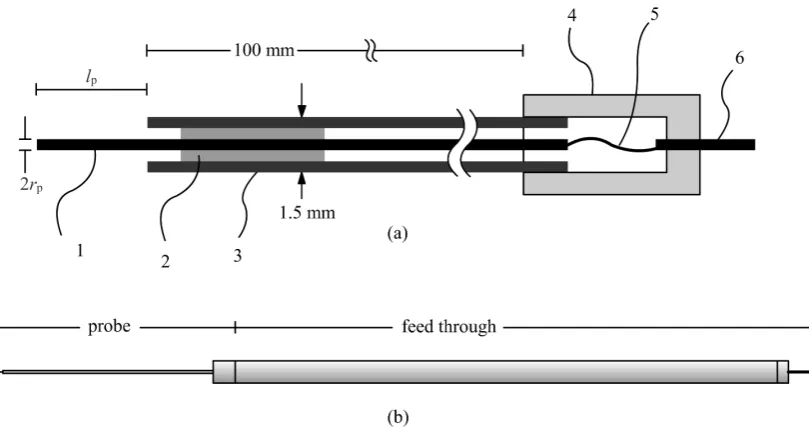
Figure 3.2: (a) A schematic diagram of the Langmuir probe consists of 1) tungsten wire, 2) inner ceramic tube, 3) outer ceramic tube, 4) probe support, 5) copper wire and 6) connector. (b) A sketch of the probe attached to a stainless-steel feedthrough.
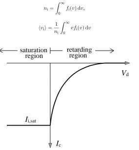
= ni, with respect to the grounded walls. When Vb is much higher than Φ, ions are repelled from the probe due to a large positive potential at the probe while electrons are attracted to the probe. In the electron saturation region, the probe current is ideally constant at a level ofIe,sat which is then related to the electron flux (Γe) arriving at the probe. If theVb is less than the Φ, electrons are partially repelled back to the plasma. The probe current decreases fromIe,sat toIp = 0, i.e. Ie =Ii, at the floating potential (Vf). In other word the floating potential Vf may be defined as the probe potential at which the electron flux to the probe is identical with the ion flux. The function of the probe current in the electron retarding region can yield the electron temperature (Te) as well as electron energy distribution functions (EEDFs). WhenVb is much less than Φ, in the ion saturation region, the negative potential at the probe almost stops the electrons from the plasma allowing only ions to flow to the probe. The probe current as a function ofVb in the ion saturation region depends on geometry of the probe and the theory used to describe the ion motion and collection [65].
3.2.2 Probe design
be determined directly from the saturation regions of the I-V characteristic without the knowledge of electron temperature.
Figure 3.2(a) is a schematic diagram of a cylindrical Langmuir probe consisting of (1) a tungsten wire, (2) an inner ceramic tube, (3) an outer ceramic tube, (4) a probe support, (5) a copper wire and (6) a connector. The tungsten wire has a radius (rp) of 0.05 mm with a protruding length (lp) between 3 mm and 6 mm from the end of the outer ceramic tube. The wire forming this tip was held in place by an inner ceramic tube situated in the outer ceramic tube so forming a re-entrant structure. The re-entrant structure of probe tip reduced problems of deposition flux short-circuiting the probe current to ground through the surface of the outer ceramic tube. The outer ceramic tube had a radius of 1.5 mm and a length of 100 mm, and was attached to the front of probe support. In addition, the tungsten wire was connected to the connector, located at the back of the support, using a copper wire. The probe in figure3.2(a) was attached to a stainless-steel feedthrough (∼1 m long) as sketched in figure3.2(b).
To be able to assume collision-less sheath conditions and therefore a simple probe analysis, the probe radius and the Debye screening length,λDe = (0Te/ene)1/2, should be less than both the electron-neutral λen and ion-neutral λin mean-free-paths [66,
67]. In HiPIMS discharges, with plasma densities varying typically between 109 to 1012cm−3, one calculates that λDe ∼0.010 – 0.19 mm, λen ∼20 – 117 mm, λin ∼9 – 27 mm for electron energies typically between 5 and 100 eV and therefore the conditions λen/λDe,λin/λDe >1 are satisfied.
3.2.3 Data analysis
Using information from the probe characteristic, basic plasma parameters including the floating potential (Vf), the plasma potential (Φ), the ion density (ni), the electron den-sity (ne), the electron temperature (Te) and the electron energy distribution functions (EEDFs) can be extracted as detailed in the following:
Floating potential Vf: Floating potential can be defined as a bias voltage at which
Figure 3.3: A diagram of the probe biasing technique to obtain floating potentials.
Plasma potential Φ: It is possible to use the voltage at the crossing point of
ex-trapolated line from electron retarding and electron saturation regions as the plasma potential. However, a more reliable approach to determine the plasma potential is from the bias voltage at which the second derivative of the I-V probe characteristic
d2I p/dVb2
is zero.
Ion density: The Orbital Motion Limited theory (OML) is used to interpret ion
current and ion density. For OML theory to be valid, the sheath surrounding the probe should be collision-less, which is generally valid for the conditionξ = (rp/λDe)<1 [66]. However, the OML theory has been found to hold very well even when the sheath dimensions become smaller that the probe radius [67]. In our case where 0.2< ξ <5.6, the OML theory is still valid according to [67]. Using the formulation in [66,67] the ion current Ii,OML (in the ion attracting region of the characteristic) follows the equation
Ii,OML≈ √
2
π eApni,OML s
e(Φ−Vb)
Mi , (3.1)
where e is the electron charge and Mi the ion mass, and Ap (= 2πrplp) is the probe area. Taking the square of the equation 3.1, we get
(Ii,OML)2≈ eK
MiΦ− eK
MiVb, (3.2)
and
K =2√2erplpni,OML 2
(3.3)
- 1 0 0 - 8 0 - 6 0 - 4 0 - 2 0 0 - 0 . 5 0
- 0 . 2 5 0 . 0 0 0 . 2 5 0 . 5 0 0 . 7 5 1 . 0 0
- 1 0 0 - 8 0 - 6 0 - 4 0 - 2 0 0 2 0 1 0 - 3
1 0 - 2 1 0 - 1 1 0 0 1 0 1 1 0 2
( b ) ( a )
V b [ V ]
I
p I p [ m A ]I
i , O M L
V
b [ V ]
I p
-I i,O
M L [ m A ]
s l o p e = 1 /T e
Figure 3.4: (a) An I-V characteristic of the Langmuir probe with a determined Ii,OML. (b)
The logarithm of the electron current after subtraction ofIi,OML from the total current. The
Maxwellian electron temperature can be found from the inverse of the linear part whenVb<Φ
region can yield a linear portion with a negative slope ofXwith a magnitude ofeK/Mi. Once the slopeX has been obtained from the plot of Ip2-Vb, the ion densityni,OML is then given by
ni,OML ≈ r
XMi 2e
1 2erplp
. (3.4)
Electron density: To determine the electron densities, three different analysis
meth-ods were used. Firstly, the analysis of probe current in the electron and ion saturation regions,ne,OML and ni,OML can be determined using the OML theory. Secondly, using the electron current at the plasma potential together with the electron temperature, the electron density (ne,sat) can also be calculated. This calculation approach is useful especially when there is the presence of multiple electron groups in the plasma. Their respective temperatures can be found from the electron-retarding region of the probe characteristic and used to determine the different group population densities. Thirdly, electron density can be determined from the electron energy distribution functionge(ε). The electron density calculated from EEDFs is denoted as ne,EDF. A comparison of the electron densities derived from those three methods (ne,OML,ne,sat,ne,EDF) gives a general picture of the validity of the probe methods.
Electron temperature: In each probe characteristic the ion current component
EEDF: To determine the dynamics of the electron energy distribution functions (EEDFs), the Druyvesteyn formulation was employed. The EEDF is given by
ge(V)≈ r
2eV me ·
2me e2Ap ·
d2I e
dV2, (3.5)
whereV = Φ−Vp is the voltage equivalent to the electron energyε. It is worth noting that the Savitzky-Golay method was used to smooth the electron current [68] with 15 data points in smoothing window and a polynomial order of two. The chosen smoothing window does not change significantly the form of the EEDFs in terms of the position of the most probable energy and the width of the distribution. The electron density can then be estimated from
ne,EEDF= Z ∞
0
ge(ε) d(ε). (3.6)
The effective electron temperature Teff can be found from this method via
Teff = 2 3ne,EEDF
Z ∞
0
εge(ε) d(ε). (3.7)
3.2.4 I-V Acquisition system
To obtain anI-V characteristic of the Langmuir probe, a varying voltage fromVb Φ to Vb Φ is need, accompanied with a measure of the probe current for each probe voltage value; establishing an I-V curve for a given condition. In addition, an ability to obtain theI-V curve for a specific time is vital to investigate the plasma parameters in pulsed discharges.
In the thesis, an automated acquisition system having 16 bit A-to-D resolution was used to acquire the probe data. The acquisition system (SmartProbe from Scientific System Ltd) has ability to bias the probe voltages from−95 to +95 V with a minimum voltage step of 25 mV. The maximum obtainable probe currents were 250 mA with a resolution of 0.1µA. The typical measured noise level in the current signal was∼0.5µA, with a maximum signal-to-noise ratio of less than 8%. However, a measured current of lower than 1µA is not acceptable for probe measurements.
To acquire anI-V curve for a specific of time during the discharge, a time-resolved mode was used with an optimum time-resolution of 0.5µs. In this mode, the equipment was triggered from a TTL pulse tapped off from the discharge voltage signal using a
was obtained from the average of three complete sweeps across the bias voltage range, and no smoothing of the characteristics was performed, except in the derivation of the electron energy distribution functions.
3.3
Retarding field analyser
3.3.1 Principle
A retarding field analyser (RFA) is a plasma diagnostic tool used to measure the velocity or energy distribution functions of charge particles in a sampling plasma. The RFA is essentially a planar probe in which electrons (or ions) are removed from the fluxes of charge particles travelling perpendicularly toward the probe allowing only ions (or electrons) to be collected. Using a retarding potential wall, the kinetic energy of the collected particles can be determined. Consequently, velocity or energy distribution functions of the collected particles can then be obtained.
In technological plasmas, the RFA has been extensively employed to determine the velocity distribution functions of the ions bombarding a grounded or biased substrate immersed in DC [69], RF [70–75] and pulsed plasmas [76,77] for depositing and etching applications.
The principle of the RFA, used to measure ion velocity distribution functions (IVDFs), is based on the use of electrostatic fields from a number of electrically bi-ased grids for electron repulsion and for ion energy discrimination (energy selection). Ions with a selected energy range are then collected at a collector electrode. Ion current at the collector as a function of the discriminating voltage establishes an I-V charac-teristic of the RFA. The ion velocity distribution function (IVDF) is proportional to the first derivative of the I-V characteristic of the RFA.
3.3.2 Modes of operation
shown in figure3.5(b). In this configuration, the voltage at the collector is slightly higher than that at the electron suppression grid (S). The secondary electrons created at the collector with energy of less thane(Vc−Vs) can thus return back to the collector obtaining the corrected ion current. Since the first grid of the two-gridded and the three gridded configurations are biased to the negative voltageVr, the measured IVDFs thus correspond to the distribution function of ions bombarding to a biased substrate. The additional grounded grid (G) can be added as a sampling grid for IVDFs of ions bombarding to a grounded substrate as shown in figure3.5(c).
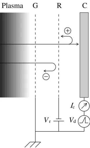
Unlike the filter mode, the discriminating voltage is applied directly to the collector when the RFA is in the normal mode of operation [70,73,79]. The diagram of a two-gridded RFA, similar in design to that used by Ingram and Braithwaite [70] is shown in figure 3.6(a). The RFA consists of a sampling grid (G), an electron repelling grid (R) and an ion collector (C). The sampling grid G is electrically grounded corresponding to a grounded substrate. The grid R is biased with a negative voltage (Vr) in order to repel electrons having energy less thane(Φ−Vr). The collector C is directly biased by a discriminating voltage (Vd). The ions with kinetic energy greater than e(Φ−Vd) are then collected and have a contribution in currentIc measured at the collector.
Obviously, operating the RFA in the normal mode is basically similar to traditional planar-type Langmuir probe measurements. It means that an acquisition system used to obtain the I-V characteristics of a Langmuir probe is compatible to obtain that of the RFA. Moreover, with the probe acquisition system as described in the previous section, IVDF for a particular time during a HiPIMS pulse can thus be measured. The RFA used in this thesis is therefore operated in the normal mode accordingly.
Vr Vd
R D S
Vr Vd
R D S C
G
Vs Vc
Vs
Vc Vc GND
Vr Vd
R D C
(a)
C
(b) (c)
Figure 3.5: Diagram of voltage distribution inside the RFA operated in the filter mode with (a) two-gridded, (b) three-gridded and (c) four-gridded configurations. The sampled ions enter to the RFA at the grid R and terminate at the collector C. The letter R denotes for the electron repelling grid, D the ion discrimination grid, C the ion collector, S electron suppressor grid, G grounded sampling grid. Voltage applied to the grid R, D, S and the collector C is denoted by
r
V
a
m
s
a
l
P
G
R
C
c [image:35.595.243.399.72.328.2]V
dFigure 3.6: A schematic diagram of the two-gridded retarding field analyser (RFA) arranged for the normal mode of operation as proposed in [70]. The RFA, immersed in a plasma having a local potential Φ, includes a sampling grid (G), a repelling grid (R) and a collector (C). The outermost grid G is electrically grounded corresponding to a grounded substrate. The grid R is biased to a negative voltageVrto repel electrons with energy of less thaneVr back to the grid
G. The collector C is connected to anI-V acquisition system at which a range of discriminating voltagesVdis scanned and the ion currentIcis measured. Only ions with kinetic energy greater
thaneVd can be collected and have a contribution in theIc measured at the collector.
3.3.3 The probe requirements
For the IVDF of ions entering the analyser not be changed on their transit through the instrument two requirements for the RFA should be satisfied as suggested by in [70,71]. Firstly, the hole size of the outermost grid or the grid G has to be small enough to prevent the penetration of the plasma into the RFA. Secondly, the total distance between the grid G and the ion collector C need to be less than the mean free path for the collision events that may alter the IVDFs. The details of these two requirements are summarised as follows.
In HiPIMS, plasma density and electron temperature at a typical substrate position (5 – 10 cm from a magnetron) is in the order of 1×1012cm−3 and 3 eV resulting inλ
De
∼13µm. The hole size of a grid used for the sampling grid should thus be less than
∼26µm for those plasma conditions.
The second requirement is associated with collision events inside the RFA. One of these events is the resonant charge exchange collisions in which an ion of one element can capture electrons from a neutral of the same element as the reaction of
Ar+fast+ Arslow→Arfast+ Ar+slow
and
Ti+fast+ Tislow →Tifast+ Ti+slow.
for argon and titanium, respectively. In these type of collisions, the fast ions along the way to the collector may change to be fast neutral and not contribute in the collector current. Therefore, total distance between the gird G and the collector C need to be less than the mean free path of those resonant charge exchange collisions.
The mean free path of the charge exchange collisions (λiex) can be obtained from the equation of
λiex= 1 nnσiex,
wherennis neutral density of an element andσiexis cross section of the charge exchange collisions between ions and neutrals of the same element. For argon and titanium ions at an energy of 0.1 eV, the cross section σiex is 72×10−20 and 220×10−20m2, respectively [80]. The neutral density of argon is ∼3.3×10¹⁹m−3 at an operating pressure of 0.133 Pa (1 mTorr). The λiex for argon and titanium is thus ∼42.1 and 13.8 mm, respectively. Therefore, the distance between the sampling gird and the collector of the RFA should be less than 13.8 mm for those process conditions.
l
sh2
l
shquasi-netural plasma
outside RFA
inside RFA
plasma sheath
a bar of the grid
Figure 3.7: A diagram showing a critical hole size of a sampling grid to prevent the plasma penetration into the RFA. The plasma with a sheath thickness oflsh, a few electron Debye length
λDe, cannot invade into the RFA if the space between bars or the hole size of the sampling grid
is less than 2lsh. However, in order to sustain a well-defined planar structure of the plasma
sheath, the hole size should be less than 2λDe. This condition is one of the crucial requirements
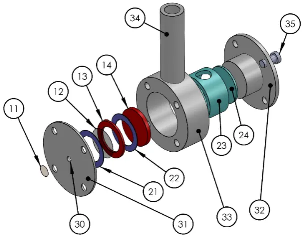
Figure 3.8: A layout presenting components of the two-gridded RFA.
3.3.4 Probe design
The RFA assembled in the present work consists of a number of components which were stacked together in a disk-like housing as presenting in figure 3.8. The detail of the RFA assembling and components are given as follows.
The RFA housing composes of three pieces of stainless steel namely a body (33) with an extruded tube (34), a front cap (31) with a 1.5 mm aperture (30) and an end cap (32). A sampling grid (11) is concentrically placed on top of the front cap (31). The front (31) and end cap (32) can firmly compress all components inside the RFA using four M2 screws (35) for each cap. The machinable insulators (23) and (24) are used to align and to electrically isolate electrodes inside the RFA from the housing. The essential components inside the RFA include insulator-washers (21) and (22), an electron repelling grid (12) on a metal-washer (13) and an ion collector (14). Two electric wires (not shown) inserted along the extruded tube (34) are soldered with the metal-washer (13) and the ion collector (14) allowing to apply the electron repelling voltageVr and the ion discriminating voltageVd to those electrodes, respectively.
the use of silver conductive paint. Another requirement in the RFA design is that the total distance between the sampling grid (11) and the ion collector (14) need to be less than 13.8 mm (λiex of titanium at 0.13 Pa). However, the RFA is designed to have a short total distance of 1.55±0.02 mm which is the summation of the thickness of the front cap (0.75±0.02 mm), the repelling grid (0.09±0.02 mm), two insulator-washers (2×0.13±0.02 mm) and the metal-washer (0.45±0.02 mm). With this total distance, the RFA is able to employ in plasmas operated at a maximum pressure of 1.18 Pa.
Since there are no critical requirements for the electron repelling grid (12), a rather strong mesh, made of stainless steel with a hole size of 0.14 mm and a transparency of 51%, was used for the grid (12). The mesh is placed on the metal-washer (13) and is tolerant enough to be compressed in the RFA.
The assembled RFA is mounted on a grounded feedthrough with the same axis of the extruded tube (34). With this configuration, the RFA is thus able to be translated along and rotated around the feedthrough axis. The translation and rotation of the RFA facilitate spatial-resolved and angular-resolved IVDF measurements. The feedthrough has two vacuum-shielded electrodes. Inside the vacuum, the electrodes are connected to the electrons repelling grid and ion collector. Outside the vacuum, the electrode for the grid R is biased with a negative voltage Vr from an external dc power supply. The collector electrode is connected directly to the automated commercial data acquisition system where the discriminating voltageVdis applied and the ion currentIcis measured, as shown in figure 3.6. A data set of (Vd, Ic) establishes an I-V characteristic of the RFA for specific plasma conditions in which an IVDF and other information of the sampling ions can be obtained.
3.3.5 Data analysis
A sketch of a typical collector current Ic as a function of discriminating voltage Vd or an I-V curve of the RFA is shown in figure 3.9. The I-V curve can be separated into two regions namely an ion saturation region and an ion retarding region. In the ion saturation region, all ions, in the ion velocity distribution function (IVDF), are collected at the collector resulting in a constant value which is referred to as an ion saturation current Ii,sat. In ion retarding region, only ions with kinetic energy greater than potential energy ofe(Φ−Vd) are able to reach the collector and contribute in the collector current. The Ic in this region thus gradually decreases associated with the distribution of ion velocities. A function of the velocity distribution fi(v) for singly charged ions can be obtained from the I-V curve by taking the first derivative of the collector current Ic with respect to the discriminating voltage Vd [71,79] (see AppendixA.3):
fi(v) =− Mi χe2A
dIc dVd
whereχis the total transparency of the grids used (18%). Ais the area of the aper-ture of the sampling grid (1.8×10⁻⁶m2),M
iis the ion mass (7.9×10⁻²⁶kg for an tita-nium ion, 6.6×10⁻²⁶ kg for an argon ion) ande is the elementary charge (1.6×10⁻¹⁹ C).
To obtain an IVDF curve, fi(v) from equation 3.8was suggested by Allen [81] to be plotted against the ion velocity (v) which is related to the discriminating voltageVd as
v= r
2eVd
Mi . (3.9)
The other fundamental information of the sampled ions can then be extracted from fi(v) including the density ni, most probable velocity, vi,most, mean velocity hvii, mean square velocity
v2 i
, flux Γi, energyEi, and energy density Ψifrom the following expressions [82]:
ni= Z ∞
0
fi(v) dv, (3.10)
hvii=
1 ni
Z ∞
0
vfi(v) dv (3.11)
I
cV
dsaturation
retarding
region
region
[image:39.595.187.473.308.617.2]I
i,satFigure 3.9: A simple sketch of anI-V characteristic of the RFA. Thex-axis is the discrim-inating voltageVd biased to the ion collector. They-axis presents ion current Ic measured at
the collector. Note that the Ic is assigned to be negative value for current carried by ions.
vi2
= 1 ni
Z ∞
0
v2fi(v) dv (3.12)
Γi=hviini (3.13)
Ei= 1 2Mi
v2i (3.14)
Ψi= 1 2Mi
vi2
ni (3.15)
The ion energy distribution functions (IEDF) assigned as fi(ε) were calculated from ion velocity distribution functionfi(v) using the well-known expression:
fi(ε) = 1
√
2Miεfi(v), (3.16)
whereε(=eVd) is the kinetic energy of singly charged ions. The mean ion energyhεii can then be obtained from:
hεii=
1 ni
Z ∞
0
εfi(ε) dε (3.17)
3.4
Gridded quartz crystal microbalance
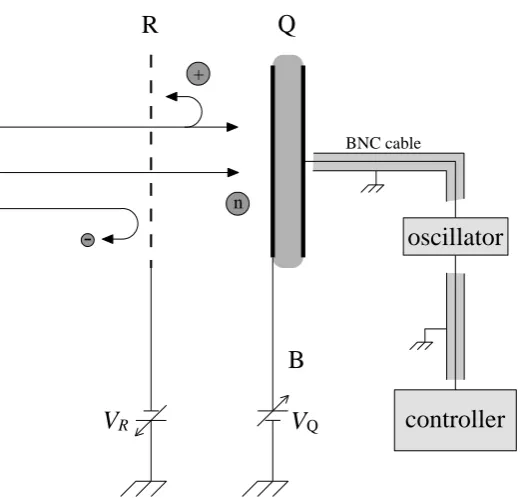
A gridded quartz crystal microbalance (g-QCM) is essentially a combination between a quartz crystal microbalance (QCM) and biasing metal grids. The g-QCM has been used to measure ionised metal flux fraction (IMFF) in ionised physical vapour deposition (IPVD) processes [83–86]. In this section, the principle and the design of g-QCM are given.
3.4.1 Principle
In conventional magnetron sputtering, depositing flux consists almost only sput-tered atoms. The thickness and the growth rate monitored by the QCM is thus caused by the neutral flux of the sputtered particles. In HiPIMS, however, a significant amount of the sputtered particles are ionised and then have a remarkable contribution in the depositing fluxes. In order to distinguish the metal ions flux and the metal neutral flux arriving to the QCM, the approach of ion repelling by the use of a positive potential with respect to the local plasma potential has essentially been adopted. The positive biasing voltage to repel the metal ion flux may be applied to the additional metal grids placed in vicinity of the QCM [83–86] or to the QCM itself [87,88].
Rossnagel and Hopwood [83] have originally employed two grids with a grounded QCM to measure IMFF in an IPVD process. The first grid was grounded to shield the QCM from the plasma, while the second grid was electrically biased to repel or admit ions to the QCM. When the grid biasing voltage is lower than the local plasma potential, the total deposition rate Rt which is the summation of metal ion deposition rate Ri and neutral deposition rate Rn can be obtained. In contrast, when biasing voltage is higher than the plasma potential, ions are repelled back allowing only neutrals to reach the QCM surface with the rate of Rn. The ionised metal flux fraction (IMFF) can principally be calculated from the total deposition rate Rt and the neutral deposition rateRn.
Greenet al.[84]and Menget al.[86] have pointed out that in order to obtain a more reliable IMFF, it is necessary to determine the geometric factor (G) of the sensor in addition to the measurement of the total deposition rateRtand the neutral deposition rate Rn. The factor G is associated with the fact that neutral deposition rate at the quartz surface is attenuated not only by the total transparency of the gird (T) used, but also by the distribution of the neutral particles and geometry of the g-QCM. IfRN is the actual deposition rate of neutrals at the first grid, the neutral deposition rate reading at the quartz surface Rn is
Rn=RN·G·T. (3.18)
Since the metal ion flux is anisotropic travelling through the plasma sheath, the depo-sition rate caused by the ionsRi at the quartz surface is reduced from the actual rate RI only by the transparency T, expressed as:
Ri=RI·T. (3.19)
If the total deposition rate measured at the quartz surfaceRtis the summation between Rn and Rior
Rt =Ri+Rn, (3.20)
the ionised metal flux fraction IMFF can be written as
IMFF = RI
RI+RN
= Rt−Rn
R
Q
oscillator
controller
BNC cable
n +
-B
[image:42.595.182.446.72.321.2]V
RV
QFigure 3.10: A schematic diagram of an in situ flux fraction analyser for metal ions. The analyser consists of an electron repelling grid (R) and a biasing quartz sensor (Q). The grid R connected to negative voltage VR is used to reduce the perturbation of the electron. For the
quartz sensor, one side of its surface, the deposited side, is biased by aVQ while the other side
is connected to the oscillator circuit via BNC cables.
It is worth noting that3.18to3.21are adopted from [86] with the assumption that the deposition rates are proportional to their depositing fluxes, e.g.,Rn∝Γn.
In order to repel ions and collect only neutrals, the voltage used to filter out the ions may bias directly to the quartz sensor. Using this technique, the number of grids used can be reduced [87] or even be eliminated [88] leading to a faster measuring rate (the thickness and growth rate at the quartz surface). In the present work, a g-QCM similar in design to that used by Nakamuraet al.[87] was adopted to achieve the fastest measuring rate. The detail of the g-QCM design is given in the next section.
3.4.2 Probe design