Rochester Institute of Technology
RIT Scholar Works
Theses Thesis/Dissertation Collections
5-2018
UVM Verification of an SPI Master Core
Deepak Siddharth Parthipan
dp9040@rit.edu
Follow this and additional works at:http://scholarworks.rit.edu/theses
This Master's Project is brought to you for free and open access by the Thesis/Dissertation Collections at RIT Scholar Works. It has been accepted for inclusion in Theses by an authorized administrator of RIT Scholar Works. For more information, please contactritscholarworks@rit.edu.
Recommended Citation
UVMVERIFICATION OF AN SPIMASTER CORE
by
Deepak Siddharth Parthipan GRADUATEPAPER
Submitted in partial fulfillment of the requirements for the degree of
MASTER OFSCIENCE
in Electrical Engineering
Approved by:
Mr. Mark A. Indovina, Lecturer
Graduate Research Advisor, Department of Electrical and Microelectronic Engineering
Dr. Sohail A. Dianat, Professor
Department Head, Department of Electrical and Microelectronic Engineering
DEPARTMENT OFELECTRICAL AND MICROELECTRONICENGINEERING
KATE GLEASONCOLLEGE OFENGINEERING
ROCHESTER INSTITUTE OF TECHNOLOGY
ROCHESTER, NEWYORK
I would like to dedicate this work to my family, my father Parthipan Kempanna Gowder, my mother Malarmathy Parthipan, my sister Vaishnavi Parthipan, and friends for their love and
Declaration
I hereby state that except where explicit references are made to the work of others, that all work and contents of this Graduate Paper are original and have not been submitted in part or whole for consideration for any other qualification in this, or any other University. This UVM Verification of an SPI Master Core Graduate Paper is the result of my work and not a collaborative work, except where explicit references are mentioned.
Acknowledgements
Abstract
Contents
Contents v
List of Figures xi
List of Tables xii
1 Introduction 1
1.1 Research Goals . . . 2
1.2 Contributions . . . 3
1.3 Organization . . . 3
2 Bibliographical Research 5 3 System Verification 8 3.1 State of the art . . . 8
3.2 UVM Overview . . . 9
3.3 UVM Class Hierarchy . . . 9
3.3.1 UVM Testbench Top . . . 10
3.3.2 UVM Test . . . 11
Contents vi
3.3.4 UVM Agent . . . 11
3.3.5 UVM Sequence Item . . . 12
3.3.6 UVM Sequence . . . 12
3.3.7 UVM Driver . . . 13
3.3.8 UVM Sequencer . . . 13
3.3.9 UVM Monitor . . . 13
3.3.10 UVM Scoreboard . . . 14
3.4 UVM Transaction Level Communication Protocol . . . 14
3.4.1 Basic Transaction Level Communication . . . 14
3.4.2 Analysis ports and Exports . . . 15
3.5 UVM Phases . . . 15
3.5.1 Build Phase . . . 15
3.5.2 Connect Phase . . . 16
3.5.3 End of Elaboration Phase . . . 17
3.5.4 Start of Simulation Phase . . . 17
3.5.5 Normal Run Phase . . . 17
3.5.6 Scheduled Run Phase . . . 17
3.5.6.1 Pre Reset Phase . . . 17
3.5.6.2 Reset Phase . . . 18
3.5.6.3 Post Reset Phase . . . 18
3.5.6.4 Pre Configure Phase . . . 18
3.5.6.5 Configure Phase . . . 18
3.5.6.6 Post Configure Phase . . . 18
3.5.6.7 Pre Main Phase . . . 18
Contents vii
3.5.6.9 Post Main Phase . . . 19
3.5.6.10 Pre Shutdown Phase . . . 19
3.5.6.11 Shutdown Phase . . . 19
3.5.6.12 Post Shutdown Phase . . . 19
3.5.7 Extract Phase . . . 19
3.5.8 Check Phase . . . 19
3.5.9 Report Phase . . . 20
3.5.10 Final Phase . . . 20
3.6 UVM Macros . . . 20
4 System Architecture 21 4.1 WISHBONE Interface . . . 21
4.2 WISHBONE I/O Registers . . . 22
4.3 Serial Peripheral Interface . . . 24
4.4 Data Transmission . . . 25
4.5 Hardware Architecture . . . 27
4.5.1 Design of Clock Generation module (spi_clk_gen) . . . 27
4.5.2 Serial data transfer module design (spi_shift) . . . 29
4.5.3 Top-level module (spi) . . . 29
4.6 SPI Registers . . . 29
4.6.1 RxX Register . . . 29
4.6.2 TxX Register . . . 30
4.6.3 ASS Register . . . 30
4.6.4 DIVIDER Register . . . 31
Contents viii
4.6.6 IE Register . . . 31
4.6.7 LSB Register . . . 31
4.6.8 Tx_NEG Register . . . 32
4.6.9 Rx_NEG Register . . . 32
4.6.10 GO_BSY Register . . . 32
4.6.11 CHAR_LEN Register . . . 32
4.7 Limitation of Standard SPI and Advancements . . . 33
5 Test Methodology and Results 34 5.1 Testbench Components . . . 34
5.1.1 Test top . . . 34
5.1.2 spi_interface . . . 35
5.1.3 spi_package . . . 36
5.1.4 spi_test . . . 36
5.1.5 spi_environment . . . 36
5.1.6 spi_agent . . . 36
5.1.7 spi_sequence_item . . . 37
5.1.8 spi_sequence . . . 37
5.1.9 spi_sequencer . . . 37
5.1.10 spi_driver . . . 38
5.1.11 spi_monitor . . . 39
5.1.12 spi_scoreboard . . . 39
5.1.13 wishbone_bfm . . . 39
5.2 Testbench Results . . . 40
Contents ix
5.2.2 Data Transactions . . . 41
5.2.2.1 WISHBONE to SPI Master communication using BFM . . . . 41
5.2.2.2 SPI Master-Slave communication . . . 41
5.2.3 Coverage . . . 42
5.2.3.1 Code Coverage . . . 43
5.2.3.2 Functional Coverage - Signal Level . . . 44
5.2.3.3 Functional Coverage - Transaction Level . . . 45
6 Conclusion 48 6.1 Future Work . . . 49
References 50 I Source Code 54 I.1 SPI Top . . . 54
I.2 SPI Clock . . . 69
I.3 SPI Shift . . . 73
I.4 Defines . . . 83
I.5 Test Top . . . 90
I.6 Interface . . . 96
I.7 Package . . . 98
I.8 Test . . . 100
I.9 Environment . . . 103
I.10 Agent . . . 105
I.11 Sequence Item . . . 108
Contents x
I.13 Sequencer . . . 113
I.14 Driver . . . 114
I.15 Monitor . . . 117
I.16 Wishbone Bus Funtion Model . . . 120
I.17 Scoreboard . . . 124
I.18 Coverage . . . 131
I.19 SPI Slave Model . . . 133
List of Figures
3.1 UVM hierarchy . . . 10
3.2 UVM Phases . . . 16
4.1 Wishbone Interface . . . 22
4.2 SPI Protocol . . . 25
4.3 Shift Register . . . 27
4.4 SPI Master Architecture . . . 28
5.1 UVM Testbench model . . . 35
5.2 UVM Sequencer Driver Communication . . . 38
5.3 WISHBONE to SPI communication . . . 42
5.4 SPI Master - Slave communication . . . 43
5.5 Top Level Code Coverage . . . 43
5.6 Clock Level Code Coverage . . . 44
5.7 Shift Level Code Coverage . . . 44
5.8 Signal Coverage . . . 45
List of Tables
4.1 WISHBONE I/O Ports . . . 23
4.2 SPI Master core registers . . . 30
5.1 Synthesis Report . . . 40
Chapter 1
Introduction
The rapid development of modern integrated circuits not only increased the complexity of inte-grated circuit (IC) design, but also made the IC verification equally challenging. Around 70% to 80% of the entire design cycle time is allotted to verification, and traditional verification method-ologies are no longer able to support current verification requirements [1]. In 2002, the Accellera Systems Initiative released SystemVerilog (SV) a a unified hardware design and verification lan-guage. SystemVerilog language was an amalgamation of constructs from different languages such as Vera, Super Log, C, Verilog and VHDL languages. Moreover, in 2005 IEEE standard-ized (1800-2005) SystemVerilog. SystemVerilog supports behavioral, register transfer level, and gate level descriptions. SystemVerilog also supports testbench development by the inclusion of object-oriented constructs, cover groups, assertions, constrained random constructs, application specific interface to other languages [2].
1.1 Research Goals 2
verification components. The verification results of this work show the effectiveness and feasi-bility of the proposed verification environment [3]
System on Chip (SoC) is used for intelligent control feature with all the integrated compo-nents connected to each other in a single chip. To complete a full system, every SoC must be linked to other system components in an efficient way that allows a faster error-free communi-cation. Data communication between core controller modules and other external devices like external EEPROMs, DACs, ADCs. is critical. Different forms of communication protocols ex-ist such as high throughput protocols like Ethernet, USB, SATA, PCI-Express which are used for data exchanges between whole systems. The Serial Peripheral Interface (SPI) is often con-sidered as light weight communication protocol. The primary purpose of the protocol is that it is suited for communication between integrated circuits for low and medium data transfer rates with onboard peripherals and the serial bus provides a significant cost advantage.
1.1
Research Goals
The goal of this research work is to build a effective test bench that validates the SPI master controller with the help of the WISHBONE bus function model and SPI slave model. The goal is achieved with the following objectives:
• To understand SPI protocol architecture and WISHBONE specific requirements, to estab-lish a connection between the test bench components and core controller.
• To apply advanced verification techniques such as Universal Verification Methodology and Coverage Driven Functional Verification.
1.2 Contributions 3
1.2
Contributions
The major contributions if this work include:
1. Research the SPI sub-system architecture, the Universal Verification Methodology, and SystemVerilog.
2. Development of a WISBONE bus function model acting as an interface between the test bench and the SPI master device under test (DUT) and SPI slave model in order to make the verification closed loop testing.
3. Build hierarchical testbench components using UVM libraries and SystemVerilog con-structs, constrained random stimulus, coverage and assertions.
4. Verify transmission of data with different character width and data formats.
1.3
Organization
The structure of the thesis is as follows:
• Chapter 2: This chapter consists majorly of articles/journals/books that are referred to provide a foundation for building a layered test bench. It also discusses some of the new methodologies and techniques for controller verification.
• Chapter3: This chapter briefly describes the system verification, various components and methodology associated with it.
1.3 Organization 4
• Chapter5: SPI test methodology, test bench components and bus function model are dis-cussed in this chapter.
Chapter 2
Bibliographical Research
SPI protocol is one of the widely used serial protocols used in a SoC compared to other protocols such UART and I2C simply because SPI can operate in higher bandwidth and throughput [4]. SPI Protocol typically provides communication between the hosts side microcontroller and slave devices. It is widely used owing to fewer control signals to operate with [5]. At the host side, the specific SPI core studied in this work acts like a WISHBONE compliant slave device. The SPI master core controller consists of three main parts, Serial shift interface, clock generator and WISHBONE interface. The SPI core controller has five 32-bit registers which can be configured through the WISHBONE interface. The serial interface consists of slave select lines, serial clock lines, as well as input and output data lines. The data transfers are full duplex in nature and number of bits per transfer is programmable [6].
6
data transfer operation, whether the data transfer has completed or not, etc. [7]. Another key feature is the flexibility of designing the SPI Interface IPs for multiple devices using parameter-ization method. Advanced design techniques, such as Time Sharing Multiplex (TSM), is used to automatically identify the master/slave devices and achieve multi-master devices. Using TSM the disadvantage of communication among multiple devices are overcome [8].
Owing to the increasing complexity of the modern SoC, the verification has become more challenging. In fact 70% of the product development time is spent on complex SoC verification. Reducing the verification effort is the key for time to market challenge. In order to cater to such growing complexity advanced verification methodologies are employed. IP verification requires in depth functional coverage with constraint random simulation technique. Various components such as coverage monitors and scoreboards are used for this purpose [9]. For a communication protocol like the SPI communication protocol, it has to be verified as per the design specifications. Applying constrained random technique for higher functional coverage provides effective verification result [10].
For many years, EDA vendors have been proposing newer verification methodologies and languages. For any system level verification methodology and language to be successful, the key lies in the scalability and reusability of the verification components developed. SystemVerilog with object-oriented programming is considered as one of the most promising techniques for high level function verification for current complex SOC designs. SystemVerilog provide com-plete verification environment, with direct and constrained random generation, assertion based verification and coverage driven metrics [11].
7
are portable and highly compatible. Such modules are called as Verification components. They are encapsulated and made ready to use configurable verification environments for full systems, submodules, or protocols. The comprehensive base class library forms the foundation for such applications. It is simulation-oriented, and performs coverage-driven constrained random verifi-cation, assertion-based verifiverifi-cation, hardware acceleration or emulation [12].
Chapter 3
System Verification
3.1
State of the art
Hardware description languages are tools used by engineers to specify abstract models of dig-ital circuits to translate them into real hardware, as the design progresses towards completion, hardware verification is performed using Hardware verification languages like SystemVerilog. The purpose of verification is to demonstrate the functional correctness of a design. Verification is achieved by means of a testbench, which is an abstract system that provides stimulus to the inputs of design under test (DUT). Functional verification shows that design implementation is in correspondence to the specification. Typically, the testbench implements a reference model of the functionality that needs to be verified and compare the results from that model with the results of the design under test. The role of functional verification is to verify if the design meets the specification but not to prove it [16].
ef-3.2 UVM Overview 9
fort is required for setting up the verification infrastructure. But as design complexity grows, it becomes a tedious and time-consuming task to write all the tests needed to cover 100% of the design. Random stimuli help to cover the unlikely cases and expose the bugs. However, in or-der to use random stimuli, the test environment requires automating process to generate random stimulus, there is a need of a block that predicts, keeps track of result and analyses them: a score-board. Additionally, functional coverage is a process used, to check what cases of the random stimulus were covered and what states of the design have been reached. This kind of testbench may require a longer time to develop, however, random based testing can actually promote the verification of the design by covering cases not achieved with directed tests [16].
3.2
UVM Overview
The UVM methodology is as a portable, open-source library from the Accellera Systems Initia-tive, and it should be compatible with any HDL simulator that supports SystemVerilog. UVM is also based on the OVM library which provides some background and maturity to the method-ology. A key feature of UVM includes re-usability though the UVM API and guidelines for a standard verification environment. The environment is easily modifiable and understood by any verification engineer that understands the methodology behind it [17].
3.3
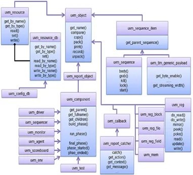
UVM Class Hierarchy
3.3 UVM Class Hierarchy 10
Figure 3.1: UVM hierarchy
3.3.1
UVM Testbench Top
3.3 UVM Class Hierarchy 11
3.3.2
UVM Test
The UVM test is the top-level UVM component class under UVM testbench. The UVM Test typically performs keys tasks like: configures values in config class and apply appropriate stim-ulus by invoking UVM sequences through the environment to the DUT. Base test class instan-tiates and configure the top-level environment; further individual tests will extend the base test to define scenario-specific environment configurations such as which sequences to run, coverage parameters, etc [18].
3.3.3
UVM Environment
The UVM environment is a container component class that groups together interrelated UVM verification components such as scoreboards, agents or even other environments. The top-level environment is a reusable component that encapsulates all the lower level verification compo-nents are targeting the DUT. There can be multiple tests that can instantiate the top-level envi-ronment class to generate and send different traffic for the selected configuration. UVM Test can override the default configuration of the top-level environment. Master UVM environment can also instantiate other child environments. Each interface to the DUT can have the sepa-rate environment. For example, UVM would be used to create reusable interface environments such as PCIe environment, USB environment, cluster environments, e.g., a CPU environment, IP interface environment, etc [18].
3.3.4
UVM Agent
3.3 UVM Class Hierarchy 12
DUT input and monitor that senses the DUT outputs. UVM agents can also include other com-ponents, like a TLM model, protocol checkers, and coverage collectors. The sequencer collects the sequences and sends to the driver. The driver then converts a transaction sequence into signal-level at DUT interface. Agent can operate in two kinds of mode active agent and passive agent. Active agent can generate stimulus, whereas passive agents only sense the DUT (sequencer and driver are disabled). Driver has a bidirectional interface to the DUT, while the Monitor has only unidirectional interface[18].
3.3.5
UVM Sequence Item
A UVM sequence item is the lowest object present under the UVM hierarchy. The sequence-item defines the transaction data items and constraints imposed on them; for example, AXI transaction and it is used to develop sequences. The concept of the transaction was created to isolate Driver from data generation but to deal with DUT interface pin wiggling activities at the bit level. UVM sequence items can include variables, constraints, and even function call for operating on themselves[18].
3.3.6
UVM Sequence
3.3 UVM Class Hierarchy 13
3.3.7
UVM Driver
A UVM Driver is a component class where the transaction-level sequence item meets the DUT clock/ bit/ pin-level activities. Driver pulls sequences from sequencer as inputs, then converts those sequences into bit-level activities, and finally drive the data onto the DUT interface ac-cording to the standard interface protocol. The functionality of driver is restricted to send the appropriate data to the DUT interface. Driver can well off course monitor the transmitted data, but that violates modularity aspects of UVM. Driver uses TLM port (seq_item_port) to receive transaction items from sequencer and use interface to drive DUT signals[18].
3.3.8
UVM Sequencer
The UVM sequencer controls request and response flow of sequence items between sequences generated and the driver component. UVM sequencer acts like an arbiter to control transaction flow from multiple sequences. UVM sequencer use TLM interface method seq_item_export and UVM driver use TLM interface method seq_item_import to connect with each other [18].
3.3.9
UVM Monitor
3.4 UVM Transaction Level Communication Protocol 14
3.3.10
UVM Scoreboard
The UVM scoreboard implements checker functionality. The checker usually verifies the DUT response against an expected DUT response. The scoreboard receives output transactions from the monitor through agent analysis ports, and can also receive expected output from a reference module. Finally, the scoreboard compares both received DUT output data versus expected data. A reference model can be written in C, C++, SystemC, or simply a SystemVerilog model. The SystemVerilog Direct Programming Interface (SystemVerilog-DPI) API is used integrate refer-ence models written in C, C++, etc., and allows them to communicate with the scoreboard [18].
3.4
UVM Transaction Level Communication Protocol
Transaction refers to a class object that includes necessary information needed for communica-tion between two components. Simple example could be a read or write transaccommunica-tion on a bus. Transaction-level modeling (TLM) is an approach that consists of multiple processes commu-nication with each other by sending transaction back and forth through channels. The channels could be FIFO or mailbox or queue. The advantages of TLM are it abstracts time, abstracts data and abstracts function.
3.4.1
Basic Transaction Level Communication
3.5 UVM Phases 15
try_peek) methods. If there are multiple transaction that needs to be communicated TLM FIFO are used. In this way the producer need not wait until consumer consumes each transaction.
3.4.2
Analysis ports and Exports
Analysis ports supports communication between one to many components. These are primarily used by coverage collectors and scoreboards. The analysis port contains analysis exports con-nected to it. When a UVM component class calls analysis port write method, then the analysis port iterates through the lists and calls write method of appropriate connected export. Similar to that of TLM FIFO Analysis ports also extends the feature to support multiple transaction.
3.5
UVM Phases
All the UVM classes in section3.3 have different simulation phases. UVM uses phases as or-dered steps of execution. Phases are implemented as methods. When deriving a new component class, the testbench simulation will go through different steps to connect, construct and configure each components of the testbench component hierarchy. Moreover, if a particular phase is not needed in some of the component class, it is possible to ignore that particular phase, and the compiler will include in its compilation process. UVM phases are represented in Figure3.2[19].
3.5.1
Build Phase
3.5 UVM Phases 16
Figure 3.2: UVM Phases
3.5.2
Connect Phase
3.5 UVM Phases 17
3.5.3
End of Elaboration Phase
Under this phase actions such as checking connections, setting up address range, initializing values or setting pointers and printing UVM testbench topology etc. are performed.
3.5.4
Start of Simulation Phase
During start of simulation environment is already configured and ready to simulate. In this phase actions such as setting initial runtime configurations, setting verbosity level of display statements, orienting UVM testbench topology to check for correctness etc., are performed.
3.5.5
Normal Run Phase
The run phase is the main execution phase, actual simulation of code will happen here. Run phase is a task and it will consume simulation time. The run phases of all components in an environment run in parallel. Any component can use either the run phase or the 12 individually scheduled phase. This phase starts at time 0. It is a better practice to use normal run phase task for drivers, monitors and scoreboards.
3.5.6
Scheduled Run Phase
Any component can use either the run phase or the 12 individually scheduled phase.
3.5.6.1 Pre Reset Phase
3.5 UVM Phases 18 3.5.6.2 Reset Phase
In this phase, the actual reset of the DUT occurs. This can be accomplished by running a se-quence at the reset interface agent. Often, the reset logic is driven from the top level itself.
3.5.6.3 Post Reset Phase
Post reset actions are done in this phase, like verifying that the device under test is in a specific state.
3.5.6.4 Pre Configure Phase
This phase determines the configuration of the device under test.
3.5.6.5 Configure Phase
Sets the device under test to the desired state as determined in pre configure phase. This would typically be register writes, table writes, memory initialization required for the device under test.
3.5.6.6 Post Configure Phase
Follows the configure phase.
3.5.6.7 Pre Main Phase
This phase executes before the main phase.
3.5.6.8 Main Phase
3.5 UVM Phases 19 3.5.6.9 Post Main Phase
Post main phase performs additional tests to verify that device under test behaved correctly based on the main phase.
3.5.6.10 Pre Shutdown Phase
This phase gets ready for shutdown.
3.5.6.11 Shutdown Phase
Shutdown phase performs all end of test checks.
3.5.6.12 Post Shutdown Phase
This phase performs anything that needs to happen after the end of checks are done. Components running in the run phase would end at the same time as the post-shutdown phase of components running in the scheduled phase mode.
3.5.7
Extract Phase
In this phase, actions such as extracting data from scoreboard and DUT (zero-time back door), preparing final statistics and closing file handlers etc. are performed.
3.5.8
Check Phase
3.6 UVM Macros 20
3.5.9
Report Phase
The reporting phase is used to furnish simulation results, also write the outputs to file.
3.5.10
Final Phase
Finally, this phase closes all file handles and display any messages.
3.6
UVM Macros
UVM macros are important aspect of the methodology. It is basically implemented methods that are useful in classes and in variables. Some of the most commonly used Marcos are:
• ‘uvm_component_utils - This macro registers is used when new ‘uvm_component classes are derived.
• ‘uvm_object_utils – Similar to ‘uvm_component_utils but instead used with ‘uvm_object. • ‘uvm_field_int - Registers a variable into factory. And implements functions like
com-pare(), print(), and copy().
• ‘uvm_info – During simulation time this macro is used to print useful messages from the UVM environment .
Chapter 4
System Architecture
4.1
WISHBONE Interface
4.2 WISHBONE I/O Registers 22
Figure 4.1: Wishbone Interface
the help of a Handshaking protocol and through the deployment of various arbitration schemes such as TDMA, Round Robin, CDMA, Token Passing, Static Priority etc. These strategies are applied based on the specific application in WISHBONE Bus [20].
4.2
WISHBONE I/O Registers
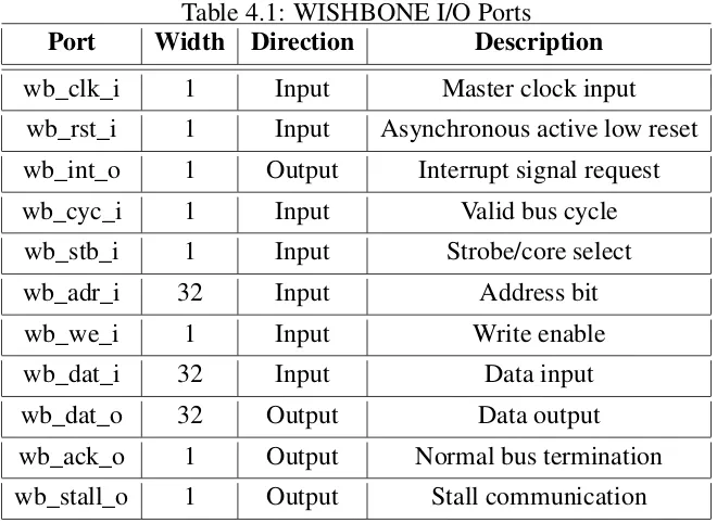
Table. 4.1 refers to the wishbone interface signals used for our Serial Peripheral Interface com-munication.
4.2 WISHBONE I/O Registers 23
Table 4.1: WISHBONE I/O Ports
Port Width Direction Description
wb_clk_i 1 Input Master clock input wb_rst_i 1 Input Asynchronous active low reset wb_int_o 1 Output Interrupt signal request wb_cyc_i 1 Input Valid bus cycle
wb_stb_i 1 Input Strobe/core select wb_adr_i 32 Input Address bit wb_we_i 1 Input Write enable wb_dat_i 32 Input Data input wb_dat_o 32 Output Data output wb_ack_o 1 Output Normal bus termination wb_stall_o 1 Output Stall communication
• wb_rst_i: wb_rst_i is active low asynchronous reset input and forces the core to restart. All internal registers are preset, to a default value and all state-machines are set to an initial state.
• wb_int_o: The interrupt request output is asserted back to the host system when the core needs its service.
• wb_cyc_i: When the cycle input wb_cyc_i is asserted, it indicates that a valid bus cycle is in progress. It needs to become true on (or before) the first wb_stb_i clock and stays true until the last wb_ack_o. The logical AND function of wb_cyc_i and wb_stb_i indicates a valid transfer cycle to/from the core. This logic is usually taken care of by the bus master. • wb_stb_i: The strobe input wb_stb_i is true for any bus transaction request. While wb_stb_i
4.3 Serial Peripheral Interface 24
• wb_adr_i: The address array input wb_adr_i passes the binary coded address to the core. The MSB is at the higher number of the array. Of the all possible 32 address lines, the slave might only be interested in the relevant slave address
• wb_we_i: When the signal wb_we_i asserted, it indicates that the current bus cycle is a write cycle. When de-asserted, it indicates that the current bus cycle is a read cycle. • wb_dat_i: The data array input wb_dat_i is used to pass binary data from the current
WISHBONE Master to the core.
• wb_dat_o: The data array output wb_dat_o is the data returned by the slave to the bus master as a result of any read request.
• wb_ack_o: When asserted, the acknowledge output wb_ack_o indicates the normal termi-nation of a valid bus cycle. There must be only one clock cycle with wb_ack_o high. • wb_stall_o: Controls the flow of data into the slave. It will be true in any cycle when
the slave can’t accept a request from the bus master, and false any time a request can be accepted. It allows the slave core to control the flow of requests that need to be serviced based on master inputs.
4.3
Serial Peripheral Interface
proto-4.4 Data Transmission 25
Figure 4.2: SPI Protocol
cols, the SPI protocol has the advantage of relatively high transmission speed, simple to use, an uses a small number of signal pins. Usually, the protocol divides devices into master and slave for transmitting and receiving the data. The protocol uses a master device to generate separate clock and data signal lines, along with a chip-select line to select the slave device for which the communication has to be established. If there is more than a slave device present, the master device must have multiple chip select interfaces to control the devices [21].
4.4
Data Transmission
The SPI bus interface consists of four logic signals lines namely Master Out Slave In (MOSI), Master In Slave Out (MISO), Serial Clock (SCLK) and Slave Select (SS).
4.4 Data Transmission 26
output signal line in a master device and as an input signal line in a slave device. It is responsible for transmission of data in one direction from master to slave.
Master In Slave Out (MISO) - The MOSI is a unidirectional signal line and configured as input signal line in a master device and as an output signal line in a slave device. It is responsible for transmission of data in one direction from slave to master. When a particular slave is not selected, the MISO line will be in high impedance state.
Slave Select (SS) - The slave select signal is used as a chip-select line to select the slave device. It is an active low signal and must stay low for the duration of the transaction.
Serial Clock (SCLK) - The serial clock line is used to synchronize data transfer between both output MOSI and input MISO signal lines. Based on the number of bytes of transactions between the Master and Slave devices, required number of bit clock cycles are generated by the master device and received as input on a slave device [3].
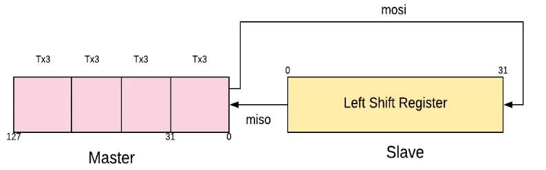
4.5 Hardware Architecture 27
Figure 4.3: Shift Register
shift register fashion and the register values are exchanged with respect to SCLK [6]. If more data needs to be exchanged, then the shift registers are loaded with new data, the and the process is repeated. Finally, after the data values are transmitted then master stops toggling the SCLK and it deselects the slave [22].
4.5
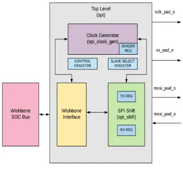
Hardware Architecture
The designed SPI Master IP core is compatible with the SPI protocol and bus principle. At the host side, the design is equivalent to the slave devices of wishbone bus specification complaint. The overall structure of the Wishbone complaint SPI Master core device can be divided into three functional units(Figure4.4): Clock generator, Serial Interface and Wishbone Interface [23].
4.5.1
Design of Clock Generation module (spi_clk_gen)
4.5 Hardware Architecture 28
Figure 4.4: SPI Master Architecture
order to ensure the reliability of timing, the clk_gen module can generate reliable serial clock transmission with odd or even frequency division in the register. Clock divider is essential part of digital ASIC and FPGA design, the idea here is to produce frequency relevant to the com-munication system. Even frequency division is achieved in order to save resources. The core generates the s_clk_o by dividing the wb_clk_i; Arbitrary clock output frequency is achieved by changing the value of the divider. The expression of s_clk_o and wb_clk_i is as follows [22].
4.6 SPI Registers 29
4.5.2
Serial data transfer module design (spi_shift)
Serial data transfer module forms the data transfer core module. It is responsible for converting input parallel data into serial output data to transmit at MOSI and convert input MISO serial data into parallel out. The Receive and Transmit register share same flip-flops. It means that what data is received from the input data line in one data transfer will be transmitted on the output line in the next transfer if no write access to the transmit register was performed between the transfers. The advantage of this is it uses fewer hardware resources, therefore, lesser power consumption. [27] SPI Master core in host side acts as a slave device to receive input data, and at the same time as the master device transmits output data [22].
4.5.3
Top-level module (spi)
The role of the top-level module is to get the basic structure of high-speed reusable SPI bus sub-components to work smoothly. Therefore, the top-level of the SPI module controls normal operation of clock generator module and serial data transmission module [22].
4.6
SPI Registers
The SPI master core uses the register [24] mentioned in the Table4.2
4.6.1
RxX Register
4.6 SPI Registers 30
Table 4.2: SPI Master core registers
Name Address Width Access Description
Rx0 0x00 32 R Data receive register 0 Rx1 0x04 32 R Data receive register 1 Rx2 0x08 32 R Data receive register 2 Rx3 0x0C 32 R Data receive register 3 Tx0 0x00 32 R/W Data transmit register 0 Tx1 0x04 32 R/W Data transmit register 1 Tx2 0x08 32 R/W Data transmit register 2 Tx3 0x0C 32 R/W Data transmit register 3 CTRL 0x10 32 R/W Control and status register DIVIDER 0x14 32 R/W Clock divider register
SS 0x18 32 R/W Slave select register bits and so on.
4.6.2
TxX Register
The Data Receive registers hold the value of data transmitted from the transfer. CTRL register holds the character length field for example if CTRL [9:3] is set to 0x10, bit TxL[15:0] holds the received data. Registers Tx1, Tx2 and Tx3 are not used If character length is less or equal to 32 bits, likewise Registers Tx2 and Tx3 are not used if character length is less than 64 bits and so on.
4.6.3
ASS Register
4.6 SPI Registers 31
slave select signals are asserted and de-asserted by writing and clearing the bits in SS register.
4.6.4
DIVIDER Register
The value in this field divides the frequency of the system clock (wb_clk_i) to generate the serial clock(s_clk) on the output sclk_pad_o. The desired frequency is obtained according to equation1.
4.6.5
SS Register
When CTRL[ASS] bit is cleared, writing 0x1 to any of the bit locations of this field sets the proper ss_pad_o line to an active state and writing 0x0 sets the line back to the inactive state. When CTRL [ASS] bit is set, writing 1 to any bit location of this field will select appropriate ss_pad_o line to be automatically driven to an active state for the duration of the transfer, and will be driven to an inactive state for the rest of the time.
4.6.6
IE Register
When this bit is set, the interrupt output is set active once after a transfer is finished. The Interrupt signal is cleared after a Read or Write to any register.
4.6.7
LSB Register
4.6 SPI Registers 32
4.6.8
Tx_NEG Register
When Tx_NEG bit is set, the mosi_pad_o signal is sent on the falling edge of a sclk_pad_o clock signal, or otherwise, the mosi_pad_o signal is sent on the rising edge of sclk_pad_o.
4.6.9
Rx_NEG Register
When Rx_NEG bit is set, the miso_pad_i signal is received on the falling edge of a sclk_pad_o clock signal, or otherwise, the miso_pad_i signal is received on the rising edge of sclk_pad_o.
4.6.10
GO_BSY Register
Writing 0x1 to this bit starts the transfer and remains set during the transfer. Automatically cleared after the transfer is finished. Writing 0x0 to this bit has no effect.
4.6.11
CHAR_LEN Register
This field specifies the number of bits to be transmitted in one transfer. Can send up to 64 bits in one transfer.
CHAR_LEN = 0x01 . . . 1 bit CHAR_LEN = 0x02 . . . 2 bits . . .
4.7 Limitation of Standard SPI and Advancements 33
4.7
Limitation of Standard SPI and Advancements
Chapter 5
Test Methodology and Results
5.1
Testbench Components
The SPI master core is verified along with the SPI slave model. Initially, the SPI master and slave have configured appropriately (for example at the master end no. of bits-32, transmit-posedge, receive-negedge). The basic idea of the verification is to send data from both master and slave ends. And after the transfer is completed verify the exchanged data at both the ends. The Figure.
5.1shows the testbench module approach. Below each of the components is explained.
5.1.1
Test top
5.1 Testbench Components 35
Figure 5.1: UVM Testbench model
5.1.2
spi_interface
5.1 Testbench Components 36
5.1.3
spi_package
The package class typically includes all SystemVerilog testbench components and make the scope available to the entire build process.
5.1.4
spi_test
The test class is created by extending the uvm_test class. Then the class is registered to factory using uvm_component_utils macro. In the build phase, the lower level SPI environment class is created and configured. Instead of the run phase, the test class contains two of the twelve scheduled phases. Reset phase typically resets the device under test. The main phase used to create the sequences and start running the sequencer for the required number of tests. Whenever there needs to be a blocking phase execution, phase raise objection is invoked and like to unblock phase drop objection is used.
5.1.5
spi_environment
SPI environment is a container component containing the agent and scoreboard. It is created using uvm_env virtual base class. In the build phase components within the environment are instantiated. And in the connect phase, the connections are made between components.
5.1.6
spi_agent
5.1 Testbench Components 37
5.1.7
spi_sequence_item
The data flows through the testbench from component to component in the form of packets called as transaction class or sequence item. The SPI sequence item class is created by extending the uvm_sequence_item class. The transaction packet consists of register configuration items (control, divider, and slave select) and data items (input, output and expected) for both master and slave. Then register the class and properties to factory using uvm_object_utils macro. A constructor function is defined for the sequence item. Randomization is applied to sequence items.
5.1.8
spi_sequence
The user-defined SPI sequence class uses uvm_sequence as its virtual base class. This class is a parameterized class with the parameter being the SPI sequence item associated with this sequence. Body() method is called, and code within this method gets executed when the sequence is run. Objections are typically raised and dropped in the pre_body() and post_body() methods of a sequence. Within the body() method the register sequence items and the data sequence items are constrained randomized.
5.1.9
spi_sequencer
5.1 Testbench Components 38
Figure 5.2: UVM Sequencer Driver Communication
5.1.10
spi_driver
5.1 Testbench Components 39
5.1.11
spi_monitor
SPI monitor senses the response from the DUT. In order to monitor the data, virtual interface han-dle is passed to monitor during the build phase. The monitor is created extending uvm_monitor. Initially, the monitor waits for the first SPI data transfer to begin. Then In the forever thread, the monitor waits for the SPI data transfer to complete. SPI monitor uses WISHBONE bus function model to read the response data from DUT. The sequence-item data packet containing the actual and expected output is now broadcast to the environment using analysis write port. The monitor then waits again for a new transfer to being, and this process repeats in a loop.
5.1.12
spi_scoreboard
SPI scoreboard is the component which has transaction level checkers and coverage collec-tors to verify the functional correctness of a given DUT. Scoreboard class is extended from the uvm_scoreboard base class. TLM analysis FIFOs to connect to the monitor. In the run phase, the input packet is retrieved from the driver, while the output packet is retrieved from the monitor. Then the transaction level functional coverage method is performed using a sampling method to get the coverage. In the end, then when the report phase is invoked the results are displayed.
5.1.13
wishbone_bfm
5.2 Testbench Results 40
5.2
Testbench Results
The functional verification of the SPI core controller was carried out successfully with the fol-lowing results.
5.2.1
SPI Master Controller Synthesis Benchmarking
[image:54.612.93.520.355.657.2]The project aims to create a functional verification environment for SPI controller. For this purpose the IP core was reused from Opencores, but with some modification. The logic synthesis of the module was performed in the TSMC 180nm, 65nm and SAED 32nm technology. Area, Power and Timing of the final module were captured Table5.1
Table 5.1: Synthesis Report
Type Technology node 32 nm 65 nm 180 nm Sequential Area(µm2) 2096.68 2520.35 18990.41
Area Combinational Area(µm2) 2527.97 2209.68 17071.08
Buf/Inv Area(µm2) 314.37 71.28 1862.78
Total Area(µm2) 5847.47 4730.03 36061.50
Internal Power(µW) 32.59 47.34 335.80
Power Switching Power(µW) 1.844 3.58 74.86
Leakage Power(µW) 452.2 0.189 0.145
Total Power(µW) 486.6 51.11 410.8
5.2 Testbench Results 41
5.2.2
Data Transactions
[image:55.612.179.428.197.257.2]The results published are for below Table 5.2 configuration for a regression run of 10 Million tests.
Table 5.2: Test Configuration
Data Transfer Sent First Transmit Receive 32bit MSB posedge negedge
5.2.2.1 WISHBONE to SPI Master communication using BFM
The communication between the WISHBONE and SPI master is performed using WISHBONE bus function model. The model mainly implements read, write and reset functionalities w.r.t WISHBONE B.3 protocol. In the below Figure. 5.3 shows the WISHBONE protocol. Initially when there is a write data is involved cycle, strobe and write enable signals along with select lines of WISHBONE are asserted to 0x1 by the bus master. The WISHBONE address and data at the same time is placed on the bus. The bus model waits until a receive acknowledgment from the slave is received. Then the bus master frees the bus by terminating the cycle signal to 0x0. For example, if the control register needs to be configured, then control register address 0x10 is sent along with the data value 0x2200, referred at reference 1 in the Figure.5.3. Correspondingly, the SPI control select flag is selected, and in the next cycle, the value is written to the local control register of the device under test.
5.2.2.2 SPI Master-Slave communication
5.2 Testbench Results 42
Figure 5.3: WISHBONE to SPI communication
determines the sampling edge of send and receive signal. These two flags should have opposite values to each other since the SPI read input and write output takes place at the same single buffer in a shift register fashion. The master also configures its divider register and slave select register. Once all SPI registers are initially set up, then go flag of the control signal is asserted, which starts the transfer. The testbench uses the flag transfer in progress to synchronize driver and monitor respective forever loop part. Finally as given in Figure. 5.4 after 32 clock cycles, the transfer in progress signal is de-asserted and thus informs the end of communication for the WISHBONE interface to collect the data.
5.2.3
Coverage
5.2 Testbench Results 43
Figure 5.4: SPI Master - Slave communication
conditions have been exercised or not. 100% Functional coverage combined with 100% Code coverage indicates the exhaustiveness of the verification plan coverage.
5.2.3.1 Code Coverage
[image:57.612.110.503.543.637.2]Tools such as Cadence Integrated Metrics Centre can automatically calculate the code coverage metric. Code coverage tracks information such what lines of code or expression or block have been exercised. However, code coverage is not exhaustive and cannot detect conditions that or not present in the code. To address these deficiencies, we go for functional coverage.
Figure 5.5: Top Level Code Coverage
5.2 Testbench Results 44
[image:58.612.114.503.199.321.2]100% because not all sections of the code are covered for example for transactions above 32bit higher order SPI receive buffers are not covered. Expression coverage is 100% except for the WISHBONE interrupt acknowledgment section. Finally, toggle coverage is low because for all the input, output wires and registers possible inputs zero’s and ones are not covered.
[image:58.612.112.503.395.515.2]Figure 5.6: Clock Level Code Coverage Figure. 5.6shows the code coverage for the SPI Top level module.
Figure 5.7: Shift Level Code Coverage
Figure. 5.7 shows the code coverage for the SPI Top level module. Block coverage is less because not all possible data transfer rates are exercised.
5.2.3.2 Functional Coverage - Signal Level
5.2 Testbench Results 45
[image:59.612.97.515.133.367.2]level below three coverpoints are incorporated:
Figure 5.8: Signal Coverage
• cp_dut_mosi: In this coverpoint mosi output line between the master and slave is checked. It has two bins of low bit(0x0) and high bit(0x1). Both the bins are covered 100%
• cp_dut_miso: In this coverpoint miso output line between the master and slave is checked. It has two bins of low bit(0x0) and high bit(0x1). Both the bins are covered 100%
• cp_mosi_miso: This coverpoint gives the cross cover of the both cp_dut_mosi and cp_dut_mosi. It results in total of 2x2 bins. However, only 50% of the bins are hit because the sampling for cross cover happens at the wb_clk master clock and not the sclk clock signal.
5.2.3.3 Functional Coverage - Transaction Level
5.2 Testbench Results 46
[image:60.612.96.514.128.372.2]outputs. At SPI signal level below six coverpoints are incorporated:
Figure 5.9: Transaction Coverage
• cp_sg_mosi_in: This coverpoint exercises input packets expected master data. Auto bin max value of 50 for this coverpoint owing to reduced regression time availability. Ideally, this should be auto bin max.
• cp_sg_mosi_out: This coverpoint exercises output packets expected master data. Auto bin max value of 50 for this coverpoint owing to reduced regression time availability. Ideally, this should be auto bin max.
• cp_sg_miso_in: This coverpoint exercises input packets expected slave data. Auto bin max value of 50 for this coverpoint owing to reduced regression time availability. Ideally, this should be auto bin max.
5.2 Testbench Results 47
max value of 50 for this coverpoint owing to reduced regression time availability. Ideally, this should be auto bin max.
• cr_mosi_master: Cross cover of cp_sg_mosi_in and cp_sg_mosi_out is checked in this coverpoint. It verifies if the actual DUT output is equal to expected DUT output. Only 2% of the bins are covered because between actual and expected only one of the 50 bins would be covered and also 50/50*50=2%.
Chapter 6
Conclusion
In this work, a reusable SystemVerilog based UVM environment is created for an SPI master core controller. The verification environment is built around WISHBONE System on Chip bus thus making both core IP, and verification IP easy to integrate. Configuration capability is provided to configure the testbench to suit different protocol characteristics. The testbench enables to verify and validate the full duplex data transfer between the master core and slave core for various character lengths and data formats respectively.
6.1 Future Work 49
6.1
Future Work
• The SPI master controller can be enhanced to include First In-First-Out buffers to accept data at different clock rates.
• The SPI master controller can be extended to advanced WISHBONE B4 specification. • The tests can be further extended to other configurations of SPI master controller so that
References
[1] W. Ni and J. Zhang, “Research of reusability based on UVM verification,” in2015 IEEE
11th International Conference on ASIC (ASICON), Nov 2015, pp. 1–4.
[2] K. Fathy and K. Salah, “An Efficient Scenario Based Testing Methodology Using UVM,”
in 2016 17th International Workshop on Microprocessor and SOC Test and Verification
(MTV), Dec 2016, pp. 57–60.
[3] P. Rajashekar Reddy, P. Sreekanth, and K. Arun Kumar, “Serial Peripheral Interface-Master Universal Verification Component using UVM,”International Journal of Advanced Scien-tific Technologies in Engineering and Management Sciences, vol. 3, p. 27, 06 2017.
[4] R. Prasad and C. S. Rani, “UART IP CORE VERIFICATION BY USING UVM,” IRF International Conference, 15 2016.
[5] P. Roopesh D, P. Siddesha K, and B. M. Kavitha Narayan, “RTL DESIGN AND VERI-FICATION OF SPI MASTER-SLAVE USING UVM,”International Journal of Advanced Research in Electronics and Communication Engineering, vol. 4, p. 4, 08 2015.
[6] K. Aditya, M. Sivakumar, F. Noorbasha, and P. B. Thummalakunta, “Design and Functional Verification of A SPI Master Slave Core Using SystemVerilog,” International Journal Of
References 51
[7] N. Anand, G. Joseph, S. S. Oommen, and R. Dhanabal, “Design and implementation of a high speed Serial Peripheral Interface,” in 2014 International Conference on Advances in Electrical Engineering (ICAEE), Jan 2014, pp. 1–3.
[8] T. Liu and Y. Wang, “IP design of universal multiple devices SPI interface,” in Anti-Counterfeiting, Security and Identification (ASID), 2011 IEEE International Conference
on. IEEE, 2011, pp. 169–172.
[9] D. Ahlawat and N. K. Shukla, “DUT Verification Through an Efficient and Reusable En-vironment with Optimum Assertion and Functional Coverage in SystemVerilog,” Interna-tional Journal of Advanced Computer Science and Applications, vol. 5, no. 4, 2014. [10] N. Gopal, “SPI Controller Core: Verification,”SSRG International Journal of VLSI &
Sig-nal Processing, vol. 2, 09 2015.
[11] Z. Zhou, Z. Xie, X. Wang, and T. Wang, “Development of verification envioronment for SPI master interface using SystemVerilog,” inSignal Processing (ICSP), 2012 IEEE 11th
International Conference on, vol. 3. IEEE, 2012, pp. 2188–2192.
[12] J. Francesconi, J. A. Rodriguez, and P. M. Julian, “UVM based testbench architecture for unit verification,” inMicro-Nanoelectronics, Technology and Applications (EAMTA), 2014
Argentine Conference on. IEEE, 2014, pp. 89–94.
[13] A. K. Swain and K. Mahapatra, “Design and verification of WISHBONE bus interface for System-on-Chip integration,” inIndia Conference (INDICON), 2010 Annual IEEE. IEEE, 2010, pp. 1–4.
[14] A. K. Oudjida, M. L. Berrandjia, A. Liacha, R. Tiar, K. Tahraoui, and Y. N. Alhoumays, “Design and test of general-purpose SPI Master/Slave IPs on OPB bus,” inSystems Signals
References 52
[15] Mahendra.B.M and Ramachandra.A.C, “Bus Functional Model Verification IP Develop-ment of AXI Protocol,”International Conference on Engineering Technology and Science, vol. 3, 02 2014.
[16] P. Araujo, “Development of a reconfigurable multi-protocol verification environment using UVM methodology,”FACULDADE DE ENGENHARIA DA UNIVERSIDADE DO PORTO, pp. 1 – 149, 06 2014.
[17] C. Spear and G. Tumbush, SystemVerilog for Verification: A Guide to Learning the
Test-bench Language Features, 3rd ed. Springer Publishing Company, Incorporated, 2012.
[18] A. B. Mehta,ASIC/SoC Functional Design Verification: A Comprehensive Guide to
Tech-nologies and Methodologies, 1st ed. Springer Publishing Company, Incorporated, 2017.
[19] IEEE, “IEEE Standard for Universal Verification Methodology Language Reference Man-ual,”IEEE Std 1800.2-2017, pp. 1–472, May 2017.
[20] M. Sharma and D. Kumar, “Wishbone bus Architecture - A Survey and Comparison,”
CoRR, vol. abs/1205.1860, 2012. [Online]. Available: http://arxiv.org/abs/1205.1860
[21] IEEE, “IEEE Standard for SystemVerilog–Unified Hardware Design, Specification, and Verification Language,” IEEE Std 1800-2017 (Revision of IEEE Std 1800-2012), pp. 1– 1315, Feb 2018.
[22] D. V. Veda Patil, Vijay Dahake and E. Pinto, “Implementation of SPI Protocol in FPGA,”
International Journal Of Computational Engineering Research, vol. 3, pp. 142 – 147, 01
2013.
Periph-References 53
eral Interface,” International Journal of Engineering Development and Research (IJEDR), vol. 1, pp. 130 – 136, Dec. 2014.
[24] Srot and Simon, SPI Master core specification, 2004. [Online]. Available: https: //opencores.org/project/spi
Appendix I
Source Code
I.1
SPI Top
1 / *
2 * A u t h o r : Deepak S i d d h a r t h P a r t h i p a n 3 * RIT , NY, USA
4 * Module : s p i 5 * /
6 //−−−−−−−−−−−−−−−−−−−−−−−−−−−−−−−−−−−−−−−−−−−−−−−−−−−−−−−−−−−−−−−−−−−−−−−−−−−−−−−−−−−
7 ‘ i n c l u d e " s r c / s p i _ d e f i n e s . v " 8 ‘ i n c l u d e " s r c / t i m e s c a l e . v "
9 //−−−−−−−−−−−−−−−−−−−−−−−−−−−−−−−−−−−−−−−−−−−−−−−−−−−−−−−−−−−−−−−−−−−−−−−−−−−−−−−−−−−
I.1 SPI Top 55
12 / * Wishbone s i g n a l s * /
13 w b _ c l k _ i , w b _ r s t _ i , w b _ a d r _ i , w b _ d a t _ i , wb_dat_o , w b _ s e l _ i , 14 wb_we_i , w b _ s t b _ i , w b _ c y c _ i , wb_ack_o , w b _ e r r _ o , w b _ i n t _ o , 15
16 / * SPI s i g n a l s * /
17 s s _ p a d _ o , s c l k _ p a d _ o , m o s i _ p a d _ o , m i s o _ p a d _ i , 18
19 / * Scan I n s e r t i o n * /
20 s c a n _ i n 0 , s c a n _ e n , t e s t _ m o d e , s c a n _ o u t 0 , t i p / / , r e s e t , c l k 21 ) ;
22 /*−−−−−−−−−−−−−−−−−−−−−−−−−−−−Wishbone s i g n a l s
−−−−−−−−−−−−−−−−−−−−−−−−−−−−−−−−−−−−−−*/
23 i n p u t w b _ c l k _ i ; / / m a s t e r c l o c k i n p u t
24 i n p u t w b _ r s t _ i ; / / s y n c h r o n o u s a c t i v e h i g h r e s e t
25 i n p u t [ 4 : 0 ] w b _ a d r _ i ; / / l o w e r a d d r e s s b i t s
26 i n p u t [ 3 2−1 : 0 ] w b _ d a t _ i ; / / d a t a b u s i n p u t
27 o u t p u t [ 3 2−1 : 0 ] w b _ d a t _ o ; / / d a t a b u s o u t p u t
28 i n p u t [ 3 : 0 ] w b _ s e l _ i ; / / b y t e
I.1 SPI Top 56
29 i n p u t wb_we_i ; / / w r i t e
e n a b l e i n p u t
30 i n p u t w b _ s t b _ i ; / / s t o b e / c o r e s e l e c t s i g n a l
31 i n p u t w b _ c y c _ i ; / / v a l i d b u s c y c l e i n p u t
32 o u t p u t wb_ack_o ; / / b u s c y c l e a c k n o w l e d g e o u t p u t
33 o u t p u t w b _ e r r _ o ; / / t e r m i n a t i o n w / e r r o r
34 o u t p u t w b _ i n t _ o ; / / i n t e r r u p t r e q u e s t s i g n a l o u t p u t
35 /*−−−−−−−−−−−−−−−−−−−−−−−−−−−−−−−−−SPI s i g n a l s
−−−−−−−−−−−−−−−−−−−−−−−−−−−−−−−−−−−−−−*/
36 o u t p u t [ ‘ SPI_SS_NB−1 : 0 ] s s _ p a d _ o ; / / s l a v e
s e l e c t
37 o u t p u t s c l k _ p a d _ o ; / / s e r i a l c l o c k
38 o u t p u t m o s i _ p a d _ o ; / / m a s t e r o u t s l a v e i n
39 i n p u t m i s o _ p a d _ i ; / / m a s t e r i n s l a v e o u t
I.1 SPI Top 57
41 / / i n p u t c l k ; / / s y s t e m
c l o c k
42 i n p u t s c a n _ i n 0 ; / / t e s t s c a n mode d a t a i n p u t
43 i n p u t s c a n _ e n ; / / t e s t s c a n mode e n a b l e
44 i n p u t t e s t _ m o d e ; / / t e s t mode s e l e c t
45 o u t p u t s c a n _ o u t 0 ; / / t e s t s c a n mode d a t a o u t p u t
46 o u t p u t t i p ;
47 /*−−−−−−−−−−−−−−−−−−−−−−−−−−−−−−−−−−−−−−−−−−−−−−−−−−−−−−−−−−−−−−−−−−−−−−−−−−−−−−−−*/
48 r e g [ 3 2−1 : 0 ] w b _ d a t _ o ; 49 r e g [ 3 2−1 : 0 ] w b _ d a t ; 50 r e g wb_ack_o ; 51 r e g w b _ i n t _ o ; 52 r e g [ ‘ SPI_CTRL_BIT_NB−1 : 0 ] c t r l ; 53 r e g [ ‘ SPI_DIVIDER_LEN−1 : 0 ] d i v i d e r ; 54 r e g [ ‘ SPI_SS_NB−1 : 0 ] s s ;
55 r e g s c a n _ o u t 0 ; 56 / / I n t e r n a l s i g n a l s
I.1 SPI Top 58
58 w i r e r x _ n e g e d g e ; / / m i s o i s s a m p l e d on n e g a t i v e e d g e
59 w i r e t x _ n e g e d g e ; / / m o s i i s d r i v e n on n e g a t i v e e d g e
60 w i r e [ ‘ SPI_CHAR_LEN_BITS−1 : 0 ] c h a r _ l e n ; / / c h a r l e n
61 w i r e go ; / / go
62 w i r e l s b ; / / l s b f i r s t on l i n e
63 w i r e i e ; / /
i n t e r r u p t e n a b l e
64 w i r e a s s ; / /
a u t o m a t i c s l a v e s e l e c t
65 w i r e s p i _ d i v i d e r _ s e l ; / / d i v i d e r r e g i s t e r s e l e c t
66 w i r e s p i _ c t r l _ s e l ; / / c t r l r e g i s t e r s e l e c t
67 w i r e [ 3 : 0 ] s p i _ t x _ s e l ; / / t x _ l r e g i s t e r s e l e c t
68 w i r e s p i _ s s _ s e l ; / / s s r e g i s t e r s e l e c t
69 r e g t i p ; / /
t r a n s f e r i n p r o g r e s s
I.1 SPI Top 59
71 w i r e n e g _ e d g e ; / / r e c o g n i z e n e g e d g e o f s c l k
72 w i r e l a s t _ b i t ; / / m a r k s
l a s t c h a r a c t e r b i t
73 //−−−−−−−−−−−−−−−−−−−−−−−−−−−−−−−−−−−−−−−−−−−−−−−−−−−−−−−−−−−−−−−−−−−−−−−−−−−−−−−−−−−
74 s p i _ c l o c k _ g e n c l o c k _ g e n ( . c l k _ i n ( w b _ c l k _ i ) , . r s t ( w b _ r s t _ i ) , . go ( go ) , . e n a b l e ( t i p ) , . l a s t _ c l k ( l a s t _ b i t ) ,
75 . d i v i d e r ( d i v i d e r ) , . c l k _ o u t (
s c l k _ p a d _ o ) , . p o s _ e d g e ( p o s _ e d g e ) , 76 . n e g _ e d g e ( n e g _ e d g e ) ) ;
77 / / . s c a n _ i n 0 ( s c a n _ i n 0 ) , . s c a n _ e n (
s c a n _ e n ) , . t e s t _ m o d e ( t e s t _ m o d e ) , . s c a n _ o u t 0 ( s c a n _ o u t 0 ) , . r e s e t ( r e s e t
) , . c l k ( c l k ) ) ;
78 //−−−−−−−−−−−−−−−−−−−−−−−−−−−−−−−−−−−−−−−−−−−−−−−−−−−−−−−−−−−−−−−−−−−−−−−−−−−−−−−−−−−
79 s p i _ s h i f t s h i f t ( . c l k _ s h i f t ( w b _ c l k _ i ) , . r s t ( w b _ r s t _ i ) , . l e n ( c h a r _ l e n [ ‘ SPI_CHAR_LEN_BITS−1 : 0 ] ) ,
80 . l a t c h ( s p i _ t x _ s e l [ 3 : 0 ] & {4{ wb_we_i } } ) , . b y t e _ s e l ( w b _ s e l _ i ) , . l s b ( l s b ) ,
81 . go ( go ) , . p o s _ e d g e ( p o s _ e d g e ) , . n e g _ e d g e ( n e g _ e d g e ) , . r x _ n e g e d g e ( r x _ n e g e d g e ) , 82 . t x _ n e g e d g e ( t x _ n e g e d g e ) , . t i p ( t i p ) , . l a s t (
I.1 SPI Top 60
83 . s _ c l k ( s c l k _ p a d _ o ) , . s _ i n ( m i s o _ p a d _ i ) , . s _ o u t ( m o s i _ p a d _ o ) ) ;
84 / / . s c a n _ i n 0 ( s c a n _ i n 0 ) , . s c a n _ e n ( s c a n _ e n ) , . t e s t _ m o d e ( t e s t _ m o d e ) , . s c a n _ o u t 0 ( s c a n _ o u t 0 ) , . r e s e t ( r e s e t ) , . c l k ( c l k ) ) ;
85 /*−−−−−−−−−−−−−−−−−−−−−−−−−−−−−−−−−−A d d r e s s d e c o d e r
−−−−−−−−−−−−−−−−−−−−−−−−−−−−−−−−−−−*/
86 a s s i g n s p i _ d i v i d e r _ s e l = w b _ c y c _ i & w b _ s t b _ i & ( w b _ a d r _ i [ ‘ SPI_OFS_BITS ] == ‘ SPI_DIVIDE ) ;
87 a s s i g n s p i _ c t r l _ s e l = w b _ c y c _ i & w b _ s t b _ i & ( w b _ a d r _ i [ ‘ SPI_OFS_BITS ] == ‘ SPI_CTRL ) ;
88 a s s i g n s p i _ t x _ s e l [ 0 ] = w b _ c y c _ i & w b _ s t b _ i & ( w b _ a d r _ i [ ‘ SPI_OFS_BITS ] == ‘ SPI_TX_0 ) ;
89 a s s i g n s p i _ t x _ s e l [ 1 ] = w b _ c y c _ i & w b _ s t b _ i & ( w b _ a d r _ i [ ‘ SPI_OFS_BITS ] == ‘ SPI_TX_1 ) ;
90 a s s i g n s p i _ t x _ s e l [ 2 ] = w b _ c y c _ i & w b _ s t b _ i & ( w b _ a d r _ i [ ‘ SPI_OFS_BITS ] == ‘ SPI_TX_2 ) ;
91 a s s i g n s p i _ t x _ s e l [ 3 ] = w b _ c y c _ i & w b _ s t b _ i & ( w b _ a d r _ i [ ‘ SPI_OFS_BITS ] == ‘ SPI_TX_3 ) ;
92 a s s i g n s p i _ s s _ s e l = w b _ c y c _ i & w b _ s t b _ i & ( w b _ a d r _ i [ ‘ SPI_OFS_BITS ] == ‘ SPI_SS ) ;
93 /*−−−−−−−−−−−−−−−−−−−−−−−−−−−−−Read f r o m r e g i s t e r s
−−−−−−−−−−−−−−−−−−−−−−−−−−−−−−−−−−−−−*/
I.1 SPI Top 61
96 c a s e ( w b _ a d r _ i [ ‘ SPI_OFS_BITS ] ) 97 ‘ i f d e f SPI_MAX_CHAR_128
98 ‘ SPI_RX_0 : w b _ d a t = r x [ 3 1 : 0 ] ; 99 ‘ SPI_RX_1 : w b _ d a t = r x [ 6 3 : 3 2 ] ; 100 ‘ SPI_RX_2 : w b _ d a t = r x [ 9 5 : 6 4 ] ;
101 ‘ SPI_RX_3 : w b _ d a t = {{128−‘SPI_MAX_CHAR{1 ’ b0 } } , r x [ ‘ SPI_MAX_CHAR−1 : 9 6 ] } ;
102 ‘ e l s e
103 ‘ i f d e f SPI_MAX_CHAR_64
104 ‘ SPI_RX_0 : w b _ d a t = r x [ 3 1 : 0 ] ;
105 ‘ SPI_RX_1 : w b _ d a t = {{64−‘SPI_MAX_CHAR{1 ’ b0 } } , r x [ ‘ SPI_MAX_CHAR−1 : 3 2 ] } ;
106 ‘ SPI_RX_2 : w b _ d a t = 32 ’ b0 ; 107 ‘ SPI_RX_3 : w b _ d a t = 32 ’ b0 ; 108 ‘e l s e
109 ‘ SPI_RX_0 : w b _ d a t = {{32−‘SPI_MAX_CHAR{1 ’ b0 } } , r x [ ‘ SPI_MAX_CHAR−1 : 0 ] } ;
110 ‘ SPI_RX_1 : w b _ d a t = 32 ’ b0 ; 111 ‘ SPI_RX_2 : w b _ d a t = 32 ’ b0 ; 112 ‘ SPI_RX_3 : w b _ d a t = 32 ’ b0 ; 113 ‘ e n d i f
114 ‘ e n d i f
I.1 SPI Top 62
116 ‘ SPI_DIVIDE : w b _ d a t = {{32−‘ SPI_DIVIDER_LEN {1 ’ b0 } } , d i v i d e r } ;
117 ‘ SPI_SS : w b _ d a t = {{32−‘ SPI_SS_NB {1 ’ b0 } } , s s } ; 118 d e f a u l t :
119 w b _ d a t = 32 ’ bx ; 120 e n d c a s e
121 end
122 /*−−−−−−−−−−−−−−−−−−−−−−−−−−−−−−−−−Wb d a t a o u t
−−−−−−−−−−−−−−−−−−−−−−−−−−−−−−−−−−−−−−−−*/
123 a l w a y s @( p o s e d g e w b _ c l k _ i o r p o s e d g e w b _ r s t _ i ) 124 b e g i n
125 i f ( w b _ r s t _ i )
126 w b _ d a t _ o <= 32 ’ b0 ; 127 e l s e
128 w b _ d a t _ o <= w b _ d a t ; 129 end
130 /*−−−−−−−−−−−−−−−−−−−−−−−−−−−−−−Wb a c k n o w l e d g e
−−−−−−−−−−−−−−−−−−−−−−−−−−−−−−−−−−−−−−−−*/
131 a l w a y s @( p o s e d g e w b _ c l k _ i o r p o s e d g e w b _ r s t _ i ) 132 b e g i n
133 i f ( w b _ r s t _ i )
134 wb_ack_o <= 1 ’ b0 ; 135 e l s e
I.1 SPI Top 63
138 /*−−−−−−−−−−−−−−−−−−−−−−−−−−−−−−−−−Wb e r r o r
−−−−−−−−−−−−−−−−−−−−−−−−−−−−−−−−−−−−−−−−−−*/
139 a s s i g n w b _ e r r _ o = 1 ’ b0 ;
140 /*−−−−−−−−−−−−−−−−−−−−−−−−−−−−−−−−−I n t e r r u p t
−−−−−−−−−−−−−−−−−−−−−−−−−−−−−−−−−−−−−−−−−*/
141 a l w a y s @( p o s e d g e w b _ c l k _ i o r p o s e d g e w b _ r s t _ i ) 142 b e g i n
143 i f ( w b _ r s t _ i )
144 w b _ i n t _ o <= 1 ’ b0 ;
145 e l s e i f ( i e && t i p && l a s t _ b i t && p o s _ e d g e ) 146 w b _ i n t _ o <= 1 ’ b1 ;
147 e l s e i f ( wb_ack_o ) 148 w b _ i n t _ o <= 1 ’ b0 ; 149 end
150 /*−−−−−−−−−−−−−−−−−−−−−−−−−−−−−−−D i v i d e r r e g i s t e r
−−−−−−−−−−−−−−−−−−−−−−−−−−−−−−−−−−−−−*/
151 a l w a y s @( p o s e d g e w b _ c l k _ i o r p o s e d g e w b _ r s t _ i ) 152 b e g i n
153 i f ( w b _ r s t _ i )
154 d i v i d e r <= { ‘ SPI_DIVIDER_LEN {1 ’ b0 } } ; 155 e l s e i f ( s p i _ d i v i d e r _ s e l && wb_we_i && ! t i p ) 156 b e g i n
157 ‘ i f d e f SPI_DIVIDER_LEN_8 158 i f ( w b _ s e l _ i [ 0 ] )
I.1 SPI Top 64
160 ‘ e n d i f
161 ‘ i f d e f SPI_DIVIDER_LEN_16 162 i f ( w b _ s e l _ i [ 0 ] )
163 d i v i d e r [ 7 : 0 ] <= w b _ d a t _ i [ 7 : 0 ] ; 164 i f ( w b _ s e l _ i [ 1 ] )
165 d i v i d e r [ ‘ SPI_DIVIDER_LEN−1 : 8 ] <= w b _ d a t _ i [ ‘ SPI_DIVIDER_LEN−1 : 8 ] ;
166 ‘ e n d i f
167 ‘ i f d e f SPI_DIVIDER_LEN_24 168 i f ( w b _ s e l _ i [ 0 ] )
169 d i v i d e r [ 7 : 0 ] <= w b _ d a t _ i [ 7 : 0 ] ; 170 i f ( w b _ s e l _ i [ 1 ] )
171 d i v i d e r [ 1 5 : 8 ] <= w b _ d a t _ i [ 1 5 : 8 ] ; 172 i f ( w b _ s e l _ i [ 2 ] )
173 d i v i d e r [ ‘ SPI_DIVIDER_LEN−1 : 1 6 ] <= w b _ d a t _ i [ ‘ SPI_DIVIDER_LEN−1 : 1 6 ] ;
174 ‘ e n d i f
175 ‘ i f d e f SPI_DIVIDER_LEN_32 176 i f ( w b _ s e l _ i [ 0 ] )
177 d i v i d e r [ 7 : 0 ] <= w b _ d a t _ i [ 7 : 0 ] ; 178 i f ( w b _ s e l _ i [ 1 ] )
179 d i v i d e r [ 1 5 : 8 ] <= w b _ d a t _ i [ 1 5 : 8 ] ; 180 i f ( w b _ s e l _ i [ 2 ] )
I.1 SPI Top 65
183 d i v i d e r [ ‘ SPI_