Int. J. Electrochem. Sci., 7 (2012) 6846 - 6858
International Journal of
ELECTROCHEMICAL
SCIENCE
www.electrochemsci.org
Development of Micro-Pores Including Nano-Pores on n-Si
(100) Coated with Sparse Ag Under Dark Etching in 1.0 M
NH
4F Containing 5.0 M H
2O
2J. C. Lin1,2,*,C. L. Chuang2, C. C. Lin3, G. Lerondel3 1
Institute of Materials Science and Engineering, Central University, No.300, Jhongda Rd., Jhongli City, Taoyuan County 320, Taiwan, R.O.C
2
Department of Mechanical Engineering, National Central University, No.300, Jhongda Rd., Jhongli City, Taoyuan County 320, Taiwan, R.O.C
3 Laboratoire de Nanotechnologies et d’Instrumentation Optique, ICD, CNRS Université de Technologie de Troyes, 12 rue Marie Curie BP2060 10010 Troyes cedex, France
*
E-mail: jclincom@cc.ncu.edu.tw
Received: 19 June 2012 / Accepted: 6 July 2012 / Published: 1 August 2012
Specimens of n-type single crystalline silicon sparsely deposited with silver nano-particles on the Si (100) surfaces were put in 1.0 M NH4F + 5.0 M H2O2 to investigate their dark etching. Through examination by scanning electron microscopy (SEM), the morphology on the n-Si (100) surface etched for 1 h revealed a sparse distribution of nano-pores (10~40 nm in diameter) according to the locations of Ag-particles; however, it exhibited porous surface consisting of micro-pores (1.5~3.1μm in diameter with 15~20μm in depth) where nano-pores (100~150 nm in diameter) were embedded inside for the etching duration prolonged for 5 h. The Nyquist plot for this system indicated two typical semicircles, in which the one in response to high frequencies revealed greater diameter and the other in response to low frequencies indicated smaller diameter. By checking the chemical bonding of silicon and silica in the NH4F/H2O2 system shows two important points at 99.3 eV and 103.4 eV.
Keywords: Porous silicon; Ammonium fluoride; Metal-assist etch; Energy band diagram
1. INTRODUCTION
[7], and photonic crystals. In these areas, the etching techniques for n-type silicon require a specific anode bias voltage and light irradiation in order to form pores. In 2000, Li and Bohn developed a metal-assisted approach for chemical etching [8]. In their study, they deposited precious metals including platinum, gold, and palladium on silicon surfaces to function as metal catalysts. Wet etching in a solution of hydrofluoric acid (49 %) and hydrogen peroxide (30 %), produced a nano-porous layer without the need for applied bias voltage. In other words, at sites on silicon surface where such a suitable metal particle was deposited, etching would be strongly accelerated leading to deep channels.
Usually, hydrofluoric acid or mixtures of hydrofluoric acid/ammonium fluoride were the most common commercial pre-treatments for silicon wafers. Under different ratios of HF/NH4F, the solutions varying in pH values were used to clean silicon wafers to remove SiO2 layers. Oxidizer such as hydrogen peroxide was added into the etched solution to cause partial oxidation on the silicon surface. It was believed that the role of oxidizers was reacted with silicon to form silica and produce electron holes [9] which transfer to exposed silicon surface to react with fluoride ions this speeding up the etching process. Toxicity was a concern to perform this process because of high volatility of hydrofluoric acid even at room temperature. Single use of ammonium fluoride was safer than its combination with HF since NH4F was stable to get rid of HF-volatility [10]. However, the reactivity was quite low even the concentration of NH4F was increased up to 40% (roughly at 11.0 M) which was alkaline with the pH approximately at 8 [11, 12]. Etching studies on various crystal surfaces of silicon in 40% ammonium fluoride with the aid of anodic biases were extensively explored [13, 14]. It was seldom reported for the silicon etched in the simple NH4F solutions without the aid of electrochemical polarization. Recently, we published a work regarding dark etching of n-Si (100) silicon coated with sparse Ag-nanoparticles in the ammonium fluoride mixed with hydrogen peroxide [15]. According to the results, we concluded that hydrogen peroxide played an oxidant not only formation of silica but also generation of electron holes on the exposed n-Si (100) surface to facilitate its etching. Under detailed examination by scanning electron microscope (SEM), we found that the n-Si (100) surface tended to develop an interesting morphology in which micro-pores were formed and a few nano-pores were embedded inside the micro-pores as the etching duration was prolonged up to 5 h. This interesting morphology in this system was seldom investigated. In the present work, we intended to focus on the occasion of this special morphology. The related kinetics and responsible mechanism for this phenomenon were also of concern. Electrochemical impedance spectroscopy (EIS) was applied in this work since it provided a powerful tool to study etching kinetics of silicon [16].
2. EXPERIMENTAL DETAILS
hydrofluoric acid solution to eliminate the oxide layer from the surfaces. The specimens were dried with a purging nitrogen gas and ready for investigation.
For deposition of silver nano-particles sparsely distributed on the surface of silicon substrate, the specimens were immersed in a 150 ml bath containing silver nitrate (2.0 mM) and 0.08 M formaldehyde maintained at 25 ℃ for 10 minutes, then removed to proceed soft baking in an oven set at 80 C for 1 h to evaporate the unreacted chemical reagents and moisture, thus resulted in a firm attachment of silver nano-particles sparsely distributed on the silicon surface.
The experimental set up was established in our previous work [15]. An etching tank (80 x 50 x 60 cm3) was made of poly-tetrafluoroethylene (PTFE) with an inner volume of 150 ml. A contact area of 64 mm2 was opened on the wall of the tank to expose the specimen in contact with the etching solution. The Ag-deposited specimen was fixed by a sample holder made of pure copper (99.90 %). An indium-gallium alloy was filled between the specimen and copper clamp to form an Ohmic contact. A connecting lead with one end conducted to a potentiostat (Potentiostat/Galvanostat AutoLab EG&G2263) and the other connected to the sample which was acting as anode or working electrode. A piece of platinum (99.99 % pure) foil (dimension in 10 mm x 10 mm x 0.5 mm) was served as the counter electrode (i.e., cathode, or auxiliary electrode). A saturated calomel electrode (SCE) equipped with a salt bridge made of high density polyethylene (HDPE) capillary tube filled with saturated KCl solution employed as a reference electrode in this work. The potential data were reported against SCE in this work.
The system was considered to have been stable when the variation of open-circuit potential (OCP) was within ±10 mV in the measurement period. For minimizing the possible interference caused by concentration polarization in the measuring EIS data, we stirred the solution with a magnetic stirrer to maintain solution circulation. In the performance of EIS measurement, the frequency was varied in a range from 106 Hz to 0.1 Hz at 5 points/decade with amplitude of 50 mV. A number sets of theoretical equivalent circuits possibly governed the etching process in different mechanisms were proposed and they were simulated with the experimental EIS data by means of a commercial simulation software (Z-view, Schlumberger, England). After ruling out the irrational mechanisms and those responsible for the data beyond satisfactory fitting, we could choose an optimal equivalent circuit which should be responsible for this etching mechanism. Subsequent to etching, the surface of the substrate was washed with deionized water and dried. Through observation with field emission scanning electron microscope (FE-SEM, FEI-NNS230), we could examine the morphology on the top surface and cross-section of the specimens in detail. The equipped energy-dispersive spectrometer (EDS, Bruker Quantax 200) was used for elemental analysis. The chemical state on the silicon surface was analyzed by X-ray photoelectron spectroscopy (XPS PHI 1600).
3. RESULTS
3.1. Surface morphology of porous Si depended upon the etching duration.
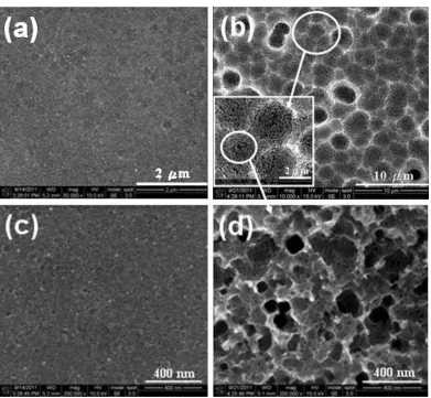
[image:4.596.104.495.195.556.2]
magnified micrograph for the location circled in Fig. 1 (a). It was seen that a number of nano-pores were formed below the locations where Ag nano-particles deposited after performance of 1h-etching. With prolonging the etching duration to 5 h, the nano-pors developed to form micro-pores (diameter in the range from 1.5~3.1μm), as shown in Fig. 1 b. Further detailed the morphology at the circled area marked in the inset of Fig. 1 b, as indicated in Fig 1 d, we found a number of nano-pores embed inside the micro-pores.
Figure 1. SE morphologies on the n-Si (100) coated with sparse Ag nanoparticles post dark etching in an aqueous solution of 1.0 M NH4F + 5.0 M H2O2 for (a) 1 h and (b) 5 h in lower magnification (X 50 k); also for (c) 1 h and (d) 5 h but in higher higher magnification (X200 k).
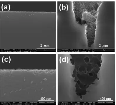
contrast, the average depth for the micro-pores resulted from prolonging etching (in 5 h) was rough at 15μm and some of them even with depth greater than 20μm, as shown in Figs. 2 b and d. The discrete pores far below the porous surface might derive from smaller sidewall pores originated from the adjacent or next vertical pores. This fact reflected the smaller pores embedded on the sidewall and bottom of the micro-pores. The absence of Ag particles might also be ascribed to the cleaning effect of the specimens prior to observation by SEM. Evidently, the diameter and depth of the pores increased with increasing the etching duration from 1 to 5 h for this system.
Figure 2. Cross-sectional SE morphologies for n-Si (100) coated with sparse Ag nanoparticles post dark etching in 1.0 M NH4F + 5.0 M H2O2 solution for (a) 1 h and (b) 5 h at lower magnifications (X50 k); also for (c) 1 h and (d) 5 h in higher magnifications (X200 k).
3.2. XPS analysis of the films
[image:5.596.103.497.213.572.2]
solution of 1M NH4F contain 5.0 M H2O2. Referring to handbook and literature, we identified the two main peaks as silicon (Si) and silica (SiO2) with their binding energy at 99.3 eV [17] and 103.4 eV [18], respectively. It was found that a few silicon oxides such as Si2O and SiO and Si2O3 in dilute but various concentrations, resultant from the curve valley between the two main peaks belonging to Si and SiO2, were involved in Fig. 3 (a). A similar result was observed but almost lack of Si2O3 in Fig. 3 (b). These results reflected the oxidation of silicon undergoes a gradual transition from 0, +1¸+2, +3 unstable valence states to reach the most stable +4 state. The peak intensity is proportional to the concentration of the oxides. Less intensity is the peak indicates the less stability of the oxide. The oxide with +1 (i.e., Si2O) valence state is the most stable spices among the intermediates. Prolonging the etching duration from 1 h to 5 h, the most unstable +3 state almost disappeared. The oxidation of silicon led to not only dissolution but also formation of silicon oxide on the specimen surface.
Figure 3. XPS for Si (2p) of the specimen etched in dark solution of 1.0 M NH4F containing 5.0 M H2O2 post (a) 1 h and (b) 5 h, respectively.
3.3. EIS of n-Si (100) at open circuit potential in 1.0 M NH4F + 5.0 M H2O2
[image:6.596.94.506.284.601.2][image:7.596.133.460.165.405.2]
solution. In Fig. 4, there existed two distinct capacitance arcs which might be ascribed to etching dissolution and the oxidation of silicon on the interface. At first glance of this plot, the magnitude of both the arcs increased with increasing the etching duration from 1 h to 5 h. The increment of the first one seemed to be greater than that of the second.
Figure 4. Nyquist plots for the wet etching of n-type silicon in the dark of 1.0 M NH4F + 5.0 M H2O2 with 1h and 5h, respectively.
4. DISCUSSION
4.1. Analysis of EIS data and equivalent circuit proposed
by a magnetic stirrer as described in the experimental section. No presence of any diffusion element in the proposed equivalent circuit may be ascribed to effective stirring in the solution. The data resulted from proposed equivalent circuit as indicated in Fig. 5 were summarized in Table 1.
Figure 5. Proposed equivalent circuit responsible for the kinetics and mechanism in the dark etched of n-Si (100) in 1.0 M NH4F + 5.0 M H2O2 solution.
Table 1. Theoretical data based on the proposed equivalent circuit which revealed the most satisfactory fitting to the EIS experimental measurements in the dark etching of Si (100) coated sparse Ag nanoparticles in 1.0 M NH4F + 5.0 M H2O2 in different durations.
Etching duration Data of the elements Symbols of elements
(unit) OCP (mV) R1 (Ω) CPE2-T (F)
CPE2-P R2 (Ω)
C3 (F)
R3 (Ω) Etching for 1h -367 125 6.7E-07 0.85 1430 0.01 400 Etching for 5h -386 150 3E-07 0.86 3250 0.004 900
3.2. Development of the reaction models for this etching system
As the specimen was immersed in the etching solution, the silicon surface free from Ag-coating was exposed to react with hydrogen peroxide and Ag-particles would catalyze the reduction of hydrogen peroxide to undergo silicon etching as described in our previous work [15]. Indirectly evident from Figs. 3 (a) and (b), we suppose that the free surface on n-Si (100) tends to form a stable film of silicon oxide (SiO2) involving a sequential steps via formation of few metastable intermediates such as Si2O (oxide of Si+), SiO (oxide of Si2+) and Si2O3(oxide of Si3+) in the following.
2 2 2 2 2
4SiH O SiOH (1.1)
2 2
2
2 4
2SiOH O SiOH (1.2)
2 3 2 2 2 2
4SiOH O SiO H (1.3)
2 2 2 2 3 2 4
2SiO H O SiO H (1.4)
[image:8.596.181.415.149.222.2]
involving formation of somewhat stable Si2O could be considered as the rate determining step in the overall reaction O H SiO O H
Si2 2 2 2 2 2 (2)
This result is consistent with that in the literature [21-24]. This silicon oxide could be dissolved in fluoride solutions to various extents depending upon fluoride concentrations [25] by obeying the equation O H SiF H HF
SiO2 6 2 6 2 2 (3)
This dissolution facilitates the exposure of silicon to contact with silver particles detached from other sites, thus undergoing another dark etching. In other words, direct dissolution of silicon occasions involving the participation of electron holes as follows
h HF SiF H
Si 4 4 4 4 (4)
6 2 4 2HF H SiF
SiF (5)
According to equation (4), the participation of electron holes leads to facilitate silicon dissolution. Occurrence of SiF4 in equation (4) tends to react with fluoride ions to form H2SiF6 that is soluble in the aqueous solution.
On the other hand, on the silicon surface coated by Ag-particles, hydrogen peroxide is catalytically reduced on the silver particles to create electron holes in the following.
H H O h
O
H2 2 2 Ag particles 2 2 2 (6)
These electron holes pass through the silver particles to reach Si-substrate thus creating anodic sits to undergo dissolution (via equations (4) and (5)) hence resulted in local etching on silicon [26]. It is obvious that all the equations from equation (2) to equation (6) summarized the electrochemical reactions resulted in dark etching of silicon in ammonium fluoride solution. Dark dissolution of silicon in ammonium fluoride via equations (2) and (3) is facilitated by dissolution of silicon oxide; however, silicon undergoes direct dark dissolution via equations (4), (5) and (6) is facilitated by holes catalytically created in the presence of Ag-particle coating on the silicon.
inclined to concentrate on the tips of the pores thus resulting in etching downwards to form vertical pores with smooth walls, as indicated in Fig. 2 (c), in the absence of side etching in the duration of 1 h. Prolonging the etching duration to 5 h, the attack on the sidewalls were inevitable, as depicted in Fig. 2 (d). Hence, nano-pores were embedded inside the micro-pores. The occasion of nano-etching on the sidewall is believed due to thickness shrinkage of the SCRs in contrast to the walls of micro-pores. It is generally accepted that the Fermi level potential (EF) of n–Si (100) is higher than the redox potential (Eredox) of the solution prior to the contact between them. As soon as they contact together, the electrons tend to flow from the higher Fermi level of n-Si (100) down to the lower redox potential level of the solution and eventually they reach the equilibrium state with identical potential (i.e., EF = Eredox) [27]. The flow of electrons leads to create excessive charges (i.e. positively charged holes) that capable of separation of those different charges distributed on the end-surfaces in the regions of the silicon which are known as the space charged regions (SCRs). The electric field induced by the SCRs leads to a downward bending of the conduction band of silicon (i.e. EC) against the conduction band at the interface (i.e., ECS) and so does the valence band of silicon (i.e., EV) against the valence band at the interface (i.e., EVS) in the same magnitude of potential shift from EF to Eredox. In contrast to the data of CPE2-T in Table 1, the capacitance is 6.7 x 10⁻⁷ F for 1 h-etching and is 3.0 x 10⁻⁷ F for 5 h-etching. A diminishment of rough 55 % in the capacitance is resultant from prolonging the duration from 1 h to 5 h.
[image:10.596.90.508.402.707.2]
This decrease in capacitance reflects less density of the charges distributed in the electric double layers, so that the electric field exerted in the SCRs is reduced, and the bending of the energy bands is significantly mitigated. Due to this fact, the positively charged holes tend to drift much readily in the sidewalls of the micro-pores whose thickness of SCRs is thinner. The probability of holes appearing at the sidewalls with thinner SCRs (at the duration of 5 h) is much greater than those with thicker SCRs (at the duration of 1 h). Consequently, the formation of nano-pores on the sidewalls of pores with longer the duration up to 5 h could be realized. Accordingly, we conclude that micro-pores with thick walls provide sufficient pathways of the holes to pass through from the Ag-coating top to the sites under various depths. On the other hand, plentiful holes are created and accumulated at the pore tip because of catalytic reduction of hydrogen peroxide with Ag-particles. The extensive attack of plentiful holes results in micro-pores; in comparison, few holes distributed on the sidewall confine to form nano-pores. Consequently, dark etching of this system gives rise to formation of micro-pores (in an average diameter of 1.5~3.1μm and depth of 15~20μm.) embedded with nano-pores (100~150 nm) under prolonging the duration up to 5 h.
3.3. Confirmation of the etching kinetics
[image:11.596.175.424.507.694.2]Figure 7 exhibited the plots of phase angle against logarithmic frequency for this system varying in etching durations. According to plots in Fig. 7, we found only two time-constant spectra centered at roughly 103~ 105 Hz and 10-1 Hz, respectively. These two spectra implied the possible formation of an oxide layer on the specimen surface [28] correlated to the kinetics occasioned at the interface. In contrast to the two curves, we found that prolonging the duration tends to increase the phase angle from 45 to 60 degree at higher frequency peak; however, no significant change in the phase angle at the lower frequency.
The evidence of oxide formation was in agreement with Niwano et al. [29]. They concluded that the thickness of the oxide layers depended on the concentration of ammonium fluoride. Under the concentration less than 10% (i.e., 2.8 M), the oxide layer was established to have a thickness that was inversely proportional to the concentration of ammonium fluoride.
4. CONCLUSIONS
Dark etching of n-Si (100) coated with sparse Ag nano-particles in 1.0 M NH4F + 5.0 M H2O2 resulted in distinct morphologies depending upon the etching duration. The silicon surface revealed a sparse distribution of nano-pores (10~40 nm in diameter) resultant from the coating Ag-spots within 1 h-etching; the surface turned into a distribution of micro-pores (1.5~3.1μm in diameter with 15~20μm in depth) in which nano-pores (100~150 nm in diameter) embedded inside for prolonging the etching up to 5 h.
EIS study was useful to explore the electrochemical kinetics and delineate the mechanism. The Nyquist plot depicted two typical semicircles in which the one centered at higher frequencies was greater than that centered at lower frequencies. The greater semicircle grew faster than the small one with increasing the etching duration. An equivalent circuit was proposed through simulation with commercial software by selecting the best fit of theoretical sets with the experimental data, we successfully constructed a schematic model to describe the dependence of etching morphology on the duration.
ACKNOWLEDGMENT
The financial support of this work by the National Science Council of the Republic of China under contract NSC-100-2221-E-008-039 is gratefully acknowledged.
References
1. A. Uhlir, Bell Syst. Tech. J., 35 (1956) 333.
2. D. R. Turner, J. Electrochem. Soc., 105 (1958) 653.
3. V. Lehmann, and U. Gruning, Thin Solid Films, 297 (1997) 13. 4. V. Lehmann, and H. Foll, J. Electrochem. Soc., 137 (1990) 653.
5. H. Ohji, P. T. J. Gennissen, P. J. French, and K. Tsutsumi, J. Micromech. Microeng., 10 (2000) 440.
6. K. J. Chao, S. C. Kao, C. M. Yang, M. S. Hseu, and T. G. Tsai, Electrochem. Solid-State Lett., 3 (2000) 489.
7. C. M. A. Ashruf, P. J. French, P. M. Sarro, R. Kazinczi, X. H. Xia, and J. J. Kelly, J. Micromech. Microeng., 10 (2000) 505.
8. X. Li, and P. W. Bohn, Appl. Phys. Lett., 77 (2000) 2572.
9. V. Kapaklis, A. Georgiopoulos, P. Poulopoulos, and C. Politis, Physica E, 38 (2007) 44. 10.J. C. Lin, C. C. Tsai, C. M. Lai, and W. C. Hsiao, “Fluoride solution in a photoelectrochemical
etching process of a silicon wafer”, U.S. Pat., 6852643 B1 (2005).
12.S. E. Bae, C. W. Lee, The Electrochemical Society, Inc., Abs. 6, 205th Meeting, (2004). 13.Y. Sawada, K. Tsujino, and M. Matsumura, J. Electrochem. Soc., 153 (2006) C854. 14.M. Lublow, and H. J. Lewerenz, Electrochem. Solid State Lett., 10 (2007) C51.
15.C. L. Chuang, J. C. Lin, K. H. Chao, C. C. Lin, and G. Lerondel, Int. J. Electrichem. Sci., 7 (2012) 2947.
16.J. C. Lin, C. M. Lai, W. D. Jehng, K. L. Hsueh, and S. L. Lee, J. Electrochem. Soc., 155 (2008) D436.
17.W. Bensch and O. Helmer, J. Phys. Chem., 99 (1995) 3326. 18.G. Hollinger and F. J. Himmpsel, Appl. Phys. Lett., 44 (1984) 93.
19.W. S. Tait, K. A. Handrich, S. W. Tait, J. W. Martin, in ASTM STP 1118, J. R. Scully, D. Silverman, M. W. Kending, Editors, American Society for Testing and materials, Philadelphia, PA., (1993) 428.
20.P. C. Searson, and X. G. Zhang, J. Electrochem. Soc., 137 (1990) 2539. 21.F. Herman, M. Schulz and G. Pensl, p. 2, Springer, Berlin, (1981). 22.S. I. Raider and A. Berman, J. Electrochem. Soc., 125 (1978) 629.
23.J. M. Aitken, and E. A. Irene, In Treatise on Materials Science and Technology, Vol.26, p.1, Academic Press, New York, (1985).
24.F. J. Himpsel, F. R. McFeely, A. Taleb-Ibrahimi and J. A. Yarmoff, Phys. Rev. B 38 (1988) 6084. 25.Z. Huang, N. Geyer, P. Werner, J. de Boor, and U. G ösele, Adv. Mater., 23 (2011) 285.
26.M. L. Chourou, K. Fukami, and T. Sakka, Electrochim. Acta, 55 (2010) 903.
27.S. R. Morrison, Electrochemistry of Semiconductor and Oxidized Metal Electrodes, Plenum Press, New York (1997).
28.W. A. Badawy, R. M. El-Sherif, and S. A. Khalil, Electrochim. Acta, 55 (2010) 8563. 29.M. Niwano, Y. Kondo, and Y. Kimura, J. Electrochem. Soc., 147 (2000) 1555.