Int. J. Electrochem. Sci., 14 (2019) 2984 – 2998, doi: 10.20964/2019.03.11
International Journal of
ELECTROCHEMICAL
SCIENCE
www.electrochemsci.org
First-Step Anodization of Commercial Aluminium in Oxalic
Acid: Role of Anodization Voltage in Tailoring the Structural
Features of Porous Alumina Film and Aluminium Substrate
S. M. Junaid Zaidi1 and M. Z. Butt2,*
1 Department of Physics, GC University, Lahore-54000, Pakistan
2 Centre for Advanced Studies in Physics, GC University, Lahore 54000, Pakistan *E-mail: [email protected]
Received: 23 June 2018 / Accepted: 19 July 2018 / Published: 7 February 2019
Commercially pure Al specimens were anodized in 0.3 M oxalic acid at 0 ºC for 15 min using five different anodization voltages in the range 10 – 50 V. Current versus time transient plots for each anodization voltage were recorded via computer interfaced multimeter. Current density, amount of charge transferred, and thickness of anodized film were found to increase linearly with the increase in anodization voltage. Scanning electron microscope studies of the first – step anodized nanoporous alumina films show that the pore diameter, interpore distance and porosity increase linearly with the increase in anodization voltage. On the contrary, the pore circularity and pore density decrease linearly with the increase in anodization voltage. XRD studies of the un-anodized and anodized Al specimens show that the peak intensity of (111), (200), and (311) planes decreases with the increase in anodization voltage whereas reverse is true for the preferentially oriented (220) plane. The nature of lattice strain is compressive (–) for the anodization voltages 20 and 50 V, as is also the case with un-anodized Al specimen, and tensile (+) for 10, 30, and 40 V.
Keywords: Anodic alumina; Anodization voltage; Film thickness; X-ray diffraction; Scanning electron microscopy; Structural features
1. INTRODUCTION
parameters with anodization temperature referred to above were linear in nature. Structural changes which occurred in the commercially pure Al substrate on anodization at different temperatures, not investigated earlier, were also explored by detailed analysis of XRD diffractographs. Their observations were in qualitative agreement with those reported in the literature for expensive high – purity Al.
As mentioned earlier, the growth and structural parameters of the nanoporous alumina films are not only dependent on the anodization temperature but also on the anodization voltage and time [1, 7 – 9]. For instance, the activation energy of the rate process of anodization of Al substrate at 50 V derived by Zaidi and Butt [1] from the Arrhenius plots of current density, charge transferred, and film thickness was 0.182 ± 0.007 eV. On the other hand, the value of activation energy of the rate process of anodization of Al substrate at 40 V, reported by Kashi and Ramazani [16], was 0.44± 0.01 eV. Similarly, the activation energy of the rate process of anodization of Al substrate at 40 V derived by Zaidi and Butt [17] from the Arrhenius plots of current density, charge transferred, and film thickness was 0.357 ± 0.013 eV, which is close to that found by Kashi and Ramazani [16]. Thus the activation energy of the rate process of anodization depends on the anodization voltage, keeping all other anodization conditions alike. The dependence of the activation energy of the rate process of anodization on the anodization voltage was accounted for by Zaidi and Butt [1] as follows. Application of higher anodization voltage facilitates the anodization process and therefore leads to reduction in the required activation energy.
To investigate the role of five different anodization voltages (10 – 50 V) in tailoring the structural and spatial features of nanoporous anodic alumina films fabricated on commercial purity Al substrate during its first – step anodization in an electrolyte of 0.3 M oxalic acid at 0 ºC for 15 min was the prime objective of the present work. Second objective was to study the effect of anodization voltage on the current – time response, current density, charge transferred, film thickness, and its growth rate. Third objective was to measure various structural parameters, namely the pore diameter, interpore distance, pore circularity, pore density, and porosity of nanoporous alumina films as a function of anodization voltage. Furthermore, structural changes which occur in the Al substrate on anodization were also investigated in detail by XRD studies of the un-anodized and anodized Al specimens.
2. EXPERIMENTAL WORK
a mixture of perchloric acid (HClO4) and C2H5OH with a ratio of 1:4 by volume at a constant current density of 500 mA cm-2 for 2 min at 10 ºC. Anodization of five specimens was carried out at 0oC for 15 min in an electrolyte of 0.3M oxalic acid (C2H2O4) contained in a glass walled anodization chamber placed inside a temperature controlled modified refrigerator. A digital thermometer was used to measure the temperature of the electrolyte during anodization process. For the sake of uniform temperature distribution, the electrolyte was stirred vigorously throughout the process of anodization using a magnetic stirrer, which has maximum stirring rate of 800 rpm. Anodization of the Al specimens was done at five different anodization voltages, namely 10, 20, 30, 40, and 50 V. The value of anodization current was monitored during the entire anodization process via computer interfaced multimeter. Complete specifications of the apparatus engaged in the electrochemical anodization setup are available in [18]. The sixth specimen was kept un-anodized for later usage as reference.
Thickness of the nanoporous anodic alumina thin films deposited on Al substrate was measured using Faraday’s Law. Scanning electron microscope (Model: JSM-6480 LV, JEOL) was used to study surface morphology of the nanoporous anodic alumina thin films. Image J software was employed to evaluate various structural parameters, namely the pore diameter (DP), interpore distance (Di), pore density (n), pore circularity, and porosity (P) from the SEM micrographs.
XRD patterns of the un-anodized and anodized Al specimens were obtained with the help of x-ray diffractometer (X’Pert PRO PANalytical) equipped with CuKα (λ = 0.154 056 nm) source. Specimens were scanned for diffraction angles in the range 30°– 90° at a scan speed of 0.133° s-1 with scan step size 0.02° and time per step 0.25 s. To investigate the structural changes occurred inside the Al substrate during the anodization process, e.g. preferred orientation of various crystallographic planes, lattice strain, and crystallite size, Harris analysis and Williamson-Hall analysis were done using the XRD patterns of the un-anodized and anodized Al specimens.
3. RESULTS AND DISCUSSION
3.1. Current ‒ Time Response
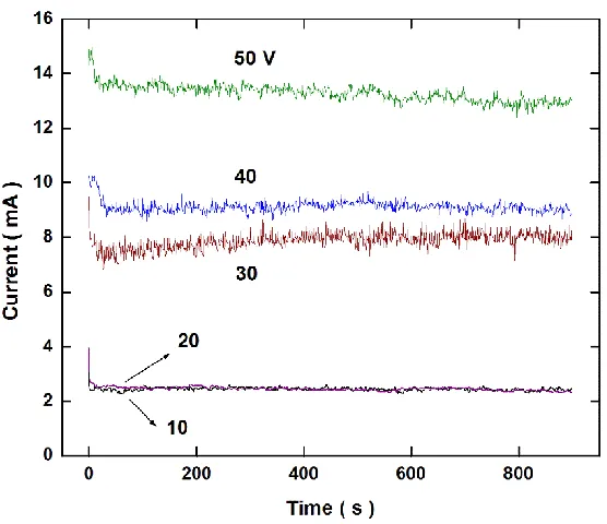
Fig. 1 denotes the current ‒ time plots of Al specimens anodized at 10, 20, 30, 40 and 50 V. It can be readily seen that when a given anodization voltage is applied, the value of anodization current momentarily increases abruptly owing to the movement of electrolyte ions towards the anode (Al specimen). Then it decreases sharply due to the formation of oxide layer on the specimen surface. On the attainment of equilibrium between oxidation and reduction processes, the current is stabilized, i.e. it becomes independent of anodization time.
Figure 1. Current ‒ time plots of Al specimens anodized at 10, 20, 30, 40, and 50 V.
3.2. Current density versus anodization voltage
It is customary to define current density of anodization J as the ratio of the total anodization current and the anodized area of specimen. The values of current density J and total charge transferred Q have been depicted by points in Fig. 2(a) and Fig. 2(b), respectively, as a function of anodization voltage. The straight lines drawn through the data points by least-squares fitting method represent a linear growth with anodization voltage in each case, and are encompassed by the mathematical expressions:
𝐽 = −0.521 + 0.128 𝑉 (1)
𝑄 = −1.011 + 0.249 𝑉 (2)
with a linear correlation coefficient r = 0.977 in each case; the value of r being close to 1 indicates an excellent linear dependence of J and Q on V. It points to a linear increase in the mobility of electrolyte ions with the anodization voltage from 10 to 50 V.
(a) (b)
Figure 2. Dependence of anodization current density (a) and charge transferred (b) on the anodization voltage of 0.3 M oxalic acid electrolyte
3.3. Film thickness analysis
The thickness (d) of nanoporous alumina films was measured by the application of Faraday’s Law [19, 20] given by:
𝑑 = 𝑄𝑀
𝑥𝑦 𝜌 𝐹𝐴 (3)
Here 𝑄 = ∫ 𝐼𝑑𝑡0𝑡 is the amount of total charge transferred, A (= 2.16 cm2) is the anodized area of the specimen, ρ (= 3.95 g cm-3) is the density of Al2O3, M (= 101.96 g mol-1) is the molecular mass of Al2O3, x is the number of Al+3 ions in Al2O3 molecule, y is the number of O-2 ions in Al2O3 molecule, and F (= 96485 C mol-1) is Faraday’s constant.
(c)
Figure 3. Film thickness as a function of (a) anodization voltage and (b) charge transferred. (c) Growth rate of anodized film as a function of current density.
The points in Fig. 3(a) and Fig. 3(b) denote the values of thickness (d) of alumina films calculated by equation (3) as a function of anodization voltage (V) and total charge transferred (Q), respectively. The straight lines passed through the data points by least-squares fitting method are represented by:
𝑑 = −0.209 + 0.051 𝑉 (4)
𝑑 = 0.075 + 0.199 𝑄 (5)
with a linear correlation coefficient r = 0.977 and 0.998, respectively. It shows that the film thickness increases linearly with the anodization voltage as well as with the total charge transferred. On the contrary, Sulka and Stepniowski [6] have observed that during the anodization of 99.995% pure Al in 0.3 M oxalic acid at rather high temperatures (20, 25, and 30 °C), the value of oxide layer thickness d increases exponentially with the anodization voltage V in the range 30 – 60 V. Again, the anodization temperature, whether low or high, determines the type of d – V dependence.
Moreover, the growth rate (nm min-1) of thin films was plotted as a function of current density J (mA cm-2) in Fig.3(c). A linear fit to the data points by least-squares fitting method shows that the growth rate (GR) of anodized films is directly proportional to the current density. Mathematically, it is encompassed by the relation:
𝐺𝑅 = −0.003 + 26.75 𝐽 (6) with a linear correlation coefficient r = 1, which is ideal.
3.4. SEM analysis
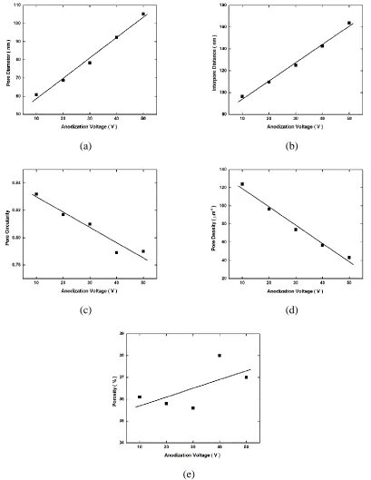
parameters on the anodization voltage has been illustrated in Fig. 5. The points denote the measured values whereas the straight lines were fitted to data points by least-squares fitting method.
(a) 10V (b) 20V
(c) 30V (d) 40V
(e) 50V
(a) (b)
(c) (d)
(e)
Figure 5. Pore diameter (a), interpore distance (b), pore circularity (c), pore density (d), and porosity (e) as a function of anodization voltage.
[image:8.596.90.499.84.613.2]
𝐷𝑃 = 47.47 + 1.12 𝑉 (7)
𝐷𝑖 = 77.23 + 1.67 𝑉 (8)
with a linear correlation coefficient r = 0.994 and 0.996, respectively.
Not only the pore size but also the pore circularity is an important structural parameter of porous anodic alumina films. It is defined as [21]:
𝐶𝑖𝑟𝑐𝑢𝑙𝑎𝑟𝑖𝑡𝑦 = 4𝜋 𝐴
𝑆2 (9)
where A and S are the area and perimeter of each pore. Circularity will be 1 if the pore shape is a perfect circle. The points in Fig. 5(c) represent the values (0.79 – 0.83) of pore circularity determined by Image J software and the straight line fitted to the data points is given by:
𝐶𝑖𝑟𝑐𝑢𝑙𝑎𝑟𝑖𝑡𝑦 = 0.841 − 0.001 𝑉 (10)
with a linear correlation coefficient r = – 0.966, which being close to 1 shows a very good linear relationship.
The values of pore density (124– 43 µm-2) were determined by means of the mathematical expression [22]:
𝑛 = 2×10⁶
√3×𝐷𝑖2 (11)
and depicted by points in Fig. 5(d). The linear fit to the data points by least-squares fitting method is embodied by the expression:
𝑛 = 139.21 − 2.01 𝑉 (12)
with a linear correlation coefficient r = - 0.990, which is very close to the ideal value 1. The decrease in pore density from 124 to 43 µm-2 with the increase in anodization voltage indicates progressive merging of pores as anodization voltage is increased from 10 to 50 V.
Finally, on using the values of pore diameter (DP) and interpore distance (Di), porosity (P) of the alumina film was determined with the help of the formula [22]:
𝑃 = 0.907 (𝐷𝑝 𝐷𝑖)
2
(13)
The points in Fig. 5(e) denote the values of porosity as a function of anodization voltage. The straight line fitted to the data points by least-squares fitting method is given by the expression:
𝑃 = 35.3 + 0.04 𝑉 (14)
with a linear correlation coefficient r = 0.636, which is reasonable. One can see an increasing trend in the porosity with the increase in anodization voltage. A comparison of Figs. 5(a) – (d) shows that an increase in pore diameter and interpore distance is accompanied by a decrease in the pore circularity and pore density. This behavior is reminiscent of that observed in the case of first – step anodization of commercial Al in oxalic acid as a function of anodization temperature T (–10 to + 30 °C) for a given anodization voltage (50 V [1], 40 V [17]) and time (15 min).
3.5. Structural characterization of anodized aluminium substrate
(a)
(b) (c)
Figure 6. (a) Combined XRD patterns of un-anodized and anodized Al specimens, (b) texture coefficient of various crystallographic planes of un-anodized and anodized Al specimens, and (c) peak intensity of various crystallographic planes of un-anodized and anodized Al specimens as a function of anodization voltage
3.5.1. Harris analysis
Harris analysis of the XRD patterns of the un-anodized and anodized Al specimens was done to find their preferred orientation using the texture coefficient formula [23, 24]:
𝑃(ℎ 𝑘 𝑙) = 𝐼(ℎ 𝑘 𝑙) 𝐼𝑜(ℎ 𝑘 𝑙)[
1
𝑛∑
𝐼(ℎ𝑘𝑙) 𝐼𝑜(ℎ𝑘𝑙)
𝑛
𝑖=1 ]
−1
(15)
been plotted as a function of 2θ in Fig. 6(b). One can see that the values of texture coefficient pertaining to (111) and (200) planes are less than 1 whereas those for (220) plane are greater than 1. However, the values of texture coefficient of (311) plane are greater than 1 for anodization voltages 0, 10, 30, and 50 V, whereas its orientation becomes non-preferential, i.e. P(311) ˂1, for anodization voltages 20 and 40 V.
Reference to Fig. 6(c) shows the dependence of peak intensity of all the four diffracting planes of the un-anodized and anodized Al specimens as a function of anodization voltage. The horizontal dotted lines represent the levels of peak intensity of (111), (200), (220), and (311) planes of the un-anodized Al specimen. For (111), (200), and (311) planes, the peak intensity decreases, in general, with the increase in anodization voltage. However, reverse is true, in general, for the (220) plane. Simulation studies of Makinson et al [25] have shown that the peak intensity of x-rays diffraction peak of a crystallographic plane depends on the concentration of point defects in it. Higher the concentration of point defects (e. g. vacancies) in the crystallographic plane, lower will be its x-ray diffraction peak intensity. One may therefore conclude that the concentration of point defects in the crystallographic planes (111), (200), and (311) increases, in general, and that in (220) plane decreases, in general, on the increase in anodization voltage from 0 to 50 V.
3.5.2. Williamson-Hall analysis
The broadening of x-ray diffraction peaks is believed to originate from (i) the crystallite size, i.e. average size of coherently diffracting domains and (ii) the lattice strain due to presence of dislocations. Williamson and Hall method [26, 27] is used to analyze the broadening of x-ray diffraction peaks to determine the crystallite size and the lattice strain. The full width at half maximum (FWHM) of a diffraction peak is given by the mathematical expression:
𝛽 = 𝛽𝐷+ 𝛽𝜀 (16)
where 𝛽𝐷 and 𝛽𝜀 are contributions to FWHM by crystallite size D and lattice strain ɛ, respectively. The peak broadening caused by crystallite size D is given by Scherrer formula 𝛽𝐷 =
𝑘𝜆 𝐷 𝐶𝑜𝑠 𝜃
, where k ≈ 0.9 is the shape factor and λ is the x − ray wavelength (= 0.15406 nm for CuKα radiation). The peak broadening due to lattice strain ɛ is given by the Wilson formula 𝛽𝜀 = 4𝜀 𝑠𝑖𝑛 𝜃 . On
substituting the values of 𝛽𝐷 and 𝛽𝜀 , equation (16) for the FWHM of a diffraction peak can be re-written as under:
𝛽 = 𝑘𝜆
𝐷 𝐶𝑜𝑠 𝜃+ 4𝜀 tan 𝜃
or
𝛽 cos 𝜃 =𝑘𝜆
𝐷 + 4𝜀 sin 𝜃 (17)
This is the well known Williamson – Hall equation. One can also re-write equation (17) in an alternate form as:
βcosθ = A + B(4sinθ) (18) where A = kλ/D and B = ε are dimensionless constants.
(a) (b)
(c) (d)
(e) (f)
Figure 7. Williamson – Hall plots of un-anodized and anodized Al specimens for various anodization voltages in the range 10 to 50 V.
Table 1. Structural data obtained by Williamson – Hall analysis
Anodization Voltage (V) A (= kλ/D) B (= ε) D (nm)
un-anodized 0.01422 -0.00051 9.8
10 -0.00248 0.00727 55.9
20 0.01599 -0.00074 8.7
30 -0.00131 0.00993 105.9
40 0.01258 0.00089 11.0
50 0.01794 -0.00156 7.7
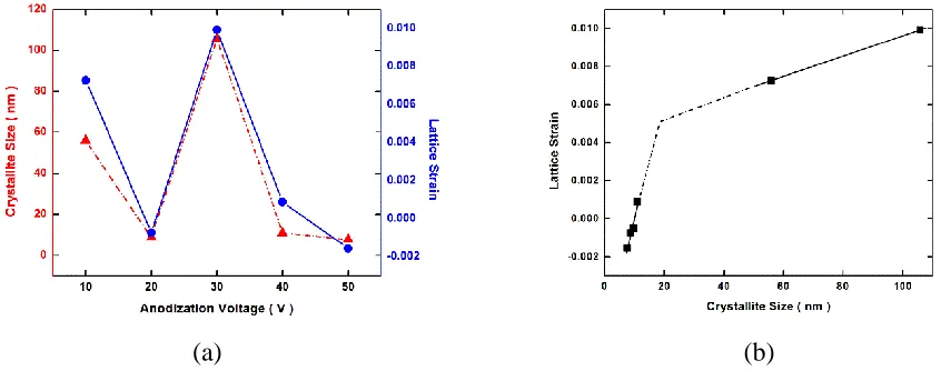
The values of crystallite size D (▲) and lattice strain ε (●), given in Table 1, for the un-anodized and anodized Al specimens have been depicted by symbols in Fig. 8(a) as a function of anodization voltage. It is evident that dependence of both D and ε on the anodization voltage is identical. However, the nature of lattice strain ε is compressive (–) for anodization voltages 20 and 50 V, as is also the case with the un-anodized Al specimen (Table 1), and tensile (+) for 10, 30, and 40 V. Finally, Fig. 8(b) illustrates the interdependence of crystallite size D and lattice strain ε. One can see that lattice strain ε varies rather rapidly with the increase in crystallite size D till D ≈ 20 nm, and slowly thereafter.
(a) (b)
Figure 8. (a) Crystallite size and lattice strain as a function of anodization voltage and (b) relationship between lattice strain and crystallite size.
4. CONCLUSIONS
[image:13.596.85.508.461.628.2]4. XRD studies of the un-anodized and anodized Al specimens show that the peak intensity of (111), (200), and (311) planes decreases with the increase in anodization voltage whereas reverse is true for the preferentially oriented (220) plane.
5. The nature of lattice strain is compressive (–) for anodization voltages 20 and 50 V, as is also the case with the un-anodized Al specimen, but tensile (+) for 10, 30, and 40 V.
ACKNOWLEDGEMENT
S. M. J. Zaidi is grateful to the Higher Education Commission, Islamabad for financial assistance under the Indigenous PhD 5000 Fellowship Program Phase-3. Athors are also grateful to the referee for his constructive criticism and valuable suggestions.
References
1. S. M. J. Zaidi and M. Z. Butt, Dig. J. Nanomater. Bios., 12 (2017) 1175. 2. G.D. Sulka and K.G. Parkoła, Electrochim. Acta, 52 (2007) 1880.
3. Y. Zuo, Y. Zhao, X. Li, N. Li, X. Bai, and S.S. Qiu, Mater. Lett., 60 (2006) 2937.
4. M. P. Proenca, C.T. Sousa, D.C Leitao, J. Ventura, J.B Sousa, and J.P Araujo, J. Non-Cryst. Solids, 354 (2008) 5238.
5. A.O. Araoyinbo, A. Rahmat, M.N. Derman, and K.R Ahmad, Adv. Mater. Lett., 3 (2012) 73. 6. G. D. Sulka and W.J. Stȩpniowski, Electrochim. Acta, 54 (2009) 3683.
7. W.J. Stȩpniowski and Z. Bojar, Surf. Coat. Technol., 206 (2011) 265.
8. S.H. Su, C.S Li, F.Bin Zhang, and M.Yokoyama , Superlattices Microstruct., 44 (2008) 514. 9. A.W. Juyana and M.N. Derman, Adv. Mater. Res., 173 (2010) 55.
10.Y. Jia, H. Zhou, P. Luo, S. Luo, J. Chen, and Y. Kuang, Surf. Coat. Technol., 201 (2006) 513. 11.U. Yogeswaran and S.M. Chen, Sensors, 8 (2008) 290.
12.Z. Huang, W. Zhang, J. Yu, and D. Gao, J. Med. Device, 1 (2007) 79. 13.A.M. Abd-Elnaiem and A. Gaber, Int. J. Electrochem. Sci., 8 (2013) 9741. 14.S. Altuntas and F. Buyukserin, Appl. Surf. Sci., 318 (2014) 290.
15.M. Jayalakshmi and K. Balasubramanian, Int. J. Electrochem. Sci., 3 (2008) 1196. 16.M.A. Kashi and A.Ramazani, J. Phys. D:Appl. Phys., 38 (2005) 2396.
17.S. M. J. Zaidi and M. Z. Butt, J. Chem. Soc. Pak.,41 (2019) in press.
18.S. M. J. Zaidi and M. Z. Butt, Designing low cost and low temperature electrochemical anodization setup to obtain metal oxide templates, International Conference on Solid State Physics, December 13 – 17, 2015, Lahore, Pakistan; Materials Today: Proceedings, Elsevier, (2018) in press.
21.C.K. Chung, M.W. Liao, H.C. Chang, and C.T. Lee, Thin Solid Films, 520 (2011) 1554. 22.G.E.J. Poinern, N. Ali, and D. Fawcett, Materials, 4 (2011) 487.
23.C.S. Barret and T.B. Massalski: Structure of Matals. Perrgamon, (1980), Oxford.
24.M.Z. Butt, D. Ali, M. Aftab, and M.U Tanveer, Surf. Topogr: Metrol.Prop., 3 (2015) 35002. 25.J.D. Makinson, J.S. Lee, S.H. Magner, R.J. De Angelis, W.N. Weins, and A.S. Hieronymus.
Advances in X-ray Analysis, 42 (2000) 407.
26.G. K. Williamson and W.H Hall, Acta Metall., 1 (1953) 22.
27.M.Z Butt, M.W Khaliq, A.M Majeed, and D. Ali, Mat. Res. Exp., 3 (2016) 096503.