Rochester Institute of Technology
RIT Scholar Works
Theses Thesis/Dissertation Collections
5-1-2008
Effects of ionizing radiation on nanomaterials and
III-V semiconductor devices.
Cory Cress
Follow this and additional works at:http://scholarworks.rit.edu/theses
Recommended Citation
EFFECTS OF IONIZING RADIATION ON
NANOMATERIALS AND III-V SEMICONDUCTOR
DEVICES
by
CORY D. CRESS
A DISSERTATION
Submitted in partial fulfillment of the requirements For the degree of Doctor of Philosophy
in
Microsystems Engineering at the
Rochester Institute of Technology
May 2008
Author: _________________________________________________________________ Microsystems Engineering Program
Certified by: _____________________________________________________________ Ryne P. Raffaelle Professor of Physics
Approved by: ____________________________________________________________ Mustafa A.G. Abushagur Director of Microsystems Engineering Program
NOTICE OF COPYRIGHT
© 2008
Cory D. Cress
REPRODUCTION PERMISSION STATEMENT
Permission Granted TITLE:
“Effects of ionizing radiation on nanomaterials and III-V semiconductor devices.”
I, Cory D. Cress, hereby grant permission to the Wallace Library of the Rochester Institute of Technology
to reproduce my dissertation in whole or in part. Any reproduction will not be for commercial use or profit.
Effects of ionizing radiation on nanomaterials and III-V
semiconductor devices
By
Cory D. Cress
Submitted by (Cory D. Cress) in partial fulfillment of the requirements for the degree of Doctor of Philosophy in Microsystems Engineering and accepted on behalf of the Rochester Institute of Technology by the dissertation committee.
We, the undersigned members of the Faculty of the Rochester Institute of Technology, certify that we have advised and/or supervised the candidate on the work described in this dissertation. We further certify that we have reviewed the dissertation manuscript and approve it in partial fulfillment of the requirements of the degree of Doctor of Philosophy in Microsystems Engineering.
Approved by:
Dr. Ryne Raffaelle
(Committee Chair and Dissertation Advisor) Date
Dr. Lynn F. Fuller
Dr. James B. Taylor
MICROSYSTEMS ENGINEERING PROGRAM ROCHESTER INSTITUTE OF TECHNOLOGY
May 2008
ABSTRACT
Kate Gleason College of Engineering Rochester Institute of Technology
Degree Doctor of Philosophy Program Microsystems Engineering__
Name of Candidate Cory D. Cress `
Title: Effects of ionizing radiation on nanomaterials and III-V semiconductor devices__
Devices based on III-V semiconductors and nanomaterials are expected to be critical components of future microsystems as the demand for greater functionality, range of application, and robustness continue to increase. There currently is a need for small-scale power supplies which can be used to power microsystems thereby enabling autonomous functionalities. The use of III-V semiconductor-based solid state devices and nanomaterials to convert the radiant energy of a radioisotope source into electricity has been investigated as a viable option to fulfill this demand. The energy imparted to a material by incident alpha-particles, resulting in electron-hole pair formation and ionization, may be converted into usable electrical power by a radioisotope microbattery (RIMB). A model describing the spatially varying rate of ionizing energy deposited in an absorber material held in close proximity to an isotropic alpha-emitting radioisotope source has been developed. The alpha-particle energy deposition model (ADEP) allows the total energy exciting the RIMB devices to be calculated and thereby provides a means to determine the efficiency of the experimentally measured devices. Two RIMB designs are investigated including a direct conversion microbattery based on a nipi-diode structure and an indirect conversion microbattery employing radioluminescent nanophosphors.
The multi-functional nature of microsystems may best be exploited by deploying them in extreme environments, such as space, where a low power consumption, small volume, and superior functionality are required. Expanding microsystems into such environments requires a full understanding of the effects that ionizing radiation will have on the optoelectronic properties of the devices and the materials which they are composed of. Irradiating devices with an isotropic alpha-particle flux is a good method for simulating the radiation damage encountered by III-V devices or nanomaterials employed in space. The large mass of alpha particles, in comparison to beta particles, leads to higher momentum transfers in nuclear interactions corresponding to a larger displacement damage dose near the surface of a material for comparably lower fluences. The effects of such irradiation on the optoelectronic properties of III-V semiconductor devices and epitaxially grown InAs quantum dots arrays are investigated. A crystal binding model based on the Tersoff interatomic potentials is developed and used to explain the increased radiation tolerance observed in the InAs quantum dot material system.
ACKNOWLEDGMENTS
I would like to thank my advisor Dr. Ryne Raffaelle, for providing me with such a great opportunity to conduct my dissertation research. From the modern facilities and instrumentation, to the breadth of research efforts I’ve had the opportunity to be exposed to, I truly believe I have had a first class research experience. These great opportunities have been afforded by his unrelenting enthusiasm in scientific research and his unsurpassed work ethic, two qualities I hope to emulate in the future.
I would also like to thank Dr. Brian Landi. As a colleague, Brian has helped me through the many trials and tribulations associated with research. He has helped to hone my research skills, and has provided me with great insight regarding publishing, presenting, and the ethics of scientific research. Socially, Brian has brought many things to my attention, like leadership skills, how to effectively influence others, and the bold and rich flavor of Excelsior 2004. It has been a pleasure to work with him over the past five years.
To my family, thank you for supporting me in all of my academic aspirations. My parents, David and Clarene Cress have been my biggest fans throughout my entire life. No issue has been too small for me to call home for advice, and no problem I’ve caused was too large for them to accept and forgive. Their belief in my abilities were expressed to me at an early age and instilled within me a desire to achieve greatness. The success that I’ve achieved until now is largely due this and to the freedom they’ve provided me in making my own decisions along the way. My enduring wife, Ania Cress has given the greatest support. Her patients during the past five years, for me to spend late nights in the laboratory or travel out of town, have been a blessing. Ania’s strong values and sense of family have given me the necessary balance in my life and has helped me overcome many hard times. She makes me a better person and for that I am greatly indebted.
To the faculty and students of the NPRL and at the NASA Glen Research Center, I am grateful for the academic and social affairs in which we’ve interacted. To Dr. Sheila Bailey, thank you for serving as my technical advisor during my NASA Graduate Student Research Program Fellowship; I am very appreciative for the funding support which was provided. To Dr. John Andersen and Dr. Seth Hubbard, thank you for your willingness to answer my seemingly endless barrage of questions. I would like to thank Christopher Schauerman for accompanying me on many trips to the gym for the necessary stress-relieving games of racquetball or to the local fishing hole for a chance to enjoy the fresh air. I am very appreciative of my committee members: Dr. Shanchieh Jay Yang, Dr. Lynn Fuller, and Dr. James Taylor, and of the following people who interacted with me throughout my education either as a mentor or a colleague: Dr. Moses Sudit, Dr. Jacqueline Mozrall, Mr. David Wilt, Mr. Paul Stiebitz, Mr. Christopher Redino, Mr. Christopher Bailey, Dr. Herbert Ruff, and Mr. Chris Evans.
TABLE OF CONTENTS
List of Figure Captions ...viii
List of Table Captions... xiv
CHAPTER 1. INTRODUCTION ... 1
CHAPTER 2. BACKGROUND INFORMATION ... 7
2.1 Radiation Interactions with Matter ... 7
2.2 Solid State Radioisotope Batteries... 13
2.3 Nanomaterials and Nano-Enhanced Devices... 22
CHAPTER 3. ADEP AND D3P MODELING ... 31
3.1 Alpha-Particle Energy Deposition Profile (ADEP) ... 31
3.2 Non-ionizing Energy Loss and D3P... 38
3.3 Energy Thresholds with Tersoff Potentials... 40
CHAPTER 4. DIRECT CONVERSION RADIOISOTOPE BATTERIES ... 45
4.1 nipi-Diode Radioisotope Battery Operation ... 45
4.2 Single Junction Device Fabrication and Testing ... 52
4.2.1 Device Fabrication ... 52
4.2.2 Alphavoltaic Battery Power Output Measurements ... 54
4.3 Selective Contacting using Smart Metallization... 58
CHAPTER 5. INDIRECT CONVERSION RADIOISOTOPE BATTERIES ... 69
5.1 Device Component Overview... 71
5.1.1 Radioluminescent Nanomaterials ... 71
5.2.1 Quantum Dot / Nanophosphor Synthesis... 80
5.2.2 InGaP2 Photovoltaic Converters ... 84
5.3 Results... 86
5.3.1 Radioluminescent Thin-Films... 86
5.3.2 CdSe QDs... 87
5.3.3 InP QDs... 89
5.3.4 Y2O3 nanophosphors... 92
5.3.5 Additional nanophosphors ... 102
5.4 ADEP Modeling of the Phosphor Films ... 103
5.5 Photovoltaic Converter Characterization... 105
5.6 Radioisotope Battery Prototype ... 107
CHAPTER 6. RADIATION AND THERMAL EFFECTS IN NANOSTRUCTURED III-V SOLAR CELLS ... 110
6.1 Quantum Dot Solar Cells (QDSC)... 110
6.1.1 Experimental... 111
6.1.2 Results and Discussion ... 112
6.1.2.1 Thermal Dependent Device Operation ... 112
6.1.2.2 Radiation Effects on Device Operation ... 117
6.2 Strain-Compensated QDSC ... 120
6.3 Strain Effects on Threshold Energy... 130
6.4 Validation of D3P Model ... 139
CHAPTER 7. CONCLUSION... 143
LIST OF FIGURE CAPTIONS
Figure 1.1 (a) Schematic depicting the loss of energy by an incident particle either through collisions with valence and core electrons or through Bremsstrahlung radiation which will be discussed in Chapter 2. (b) Schematic depicting the displacement of a lattice atom as a result of an incident particle collision. The trajectories of the Primary Knock-On (PKO) atom and the back-scattered particle are indicated. ... 4 Figure 2.1. Timeline of radioisotope devices reported in the literature since 1951. The
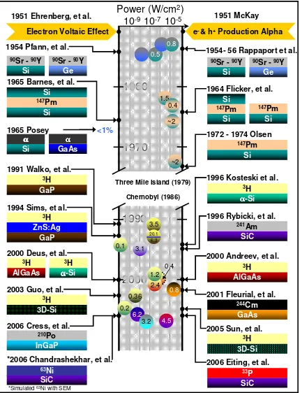
rectangles indicate the semiconductor material, radioisotope source used, and the geometry of the device, i.e., 2π vs. 4π. Down the center column is a chart (semi-log axes) depicting the power output of the device and the year in which it was reported. The markers on the chart are color coded to correspond with the device and the numbers on the marker indicate the reported (or calculated)
η
semi of the device. ... 20 Figure 2.2. Moving from left to right the schematics depict the structure underconsideration, the corresponding allowed electronic k
r
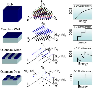
in reciprocal space, and the density of states with respect to energy for electrons referenced from the top of the valence band. Increasing confinement is depicted from the top down beginning with no confinement, 1-D, 2-D, and 3-D. ... 25 Figure 2.3. Product of the bandgap and the Bohr exciton radius for various III-V in
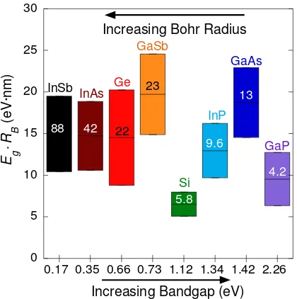
addition to Si and Ge for reference. The materials are arranged in order of
increasing bandgap... 27 Figure 3.1. Total ionization rate per unit distance for alpha-particles in InGaP2, Al, and
Air. The bottom and left axis apply for the two solids, while the top and left axis are used for air. ... 32 Figure 3.2. (a) Source – diode configuration used to measure radioisotope batteries and
to simulate the space radiation environment. (b) A cross section of the geometry in (a) used to illustrate how the flux and ADEP is calculated. ... 35
Figure 4.1: A diagram of a nipi-structured alpha voltaic battery... 46
Figure 4.2. (a) Device structure overlaid with a contour plot of the net doping in the structure, and (b) acceptor and donor doping concentration along a line directed perpendicularly into the device... 48 Figure 4.3. Contour plot depicting the donor dopant concentration near the cathode
illustrating the high doping in this region which was used to simulate the selective metallization contacting scheme. ... 49 Figure 4.4. Electric field profile near the anode contact of the simulated InGaP2nipi
-diode... 51 Figure 4.5. Veeco D125LDM OMVPE Reactor at NASA GRC used to fabricate the
active layers on the in InGaP2 devices... 53 Figure 4.6. (a) A digital photograph of a wafer after topside metallization. (b) A digital
photograph of one of the devices with ring contacts used in the study. ... 54 Figure 4.7. Current density vs. voltage for a 1 cm2 cell under 1 µCi and 1 mCi
Figure 4.9. Current density verses voltage for a 1 cell, 2 cells and 3 cells under alpha-particle flux. ... 56 Figure 4.10. Equivalent circuit structure of nipi-diode... 58
Figure 4.11. (a) Schematic depicting the structure used to test the contact resistance of p-type metallization on a p-type GaAs epitaxial layer, (b) p-type metallization deposited on an n-type epitaxial layer for rectifying contacts, and (c) transmission line measurement test structure used to determine the contact resistance for the p-type metallization on p-p-type epitaxial layers (and likewise for n-p-type metallization and n-type epitaxial layers)... 59 Figure 4.12. Resistance vs. contact spacing for p-type metallization on p-type epitaxial
layer measured on TLM structure. The contract resistance was found to be about 0.16 Ω. ... 60 Figure 4.13. (a) First quadrant semi-log plot of the current vs. voltage characterizes for
the p-type metallization contacts on n-type epitaxial layer post annealing at 400 °C; (b) contains the full I-V characteristics. ... 61 Figure 4.14. (a) SEM images depicting the formation of the V-grooves with increased
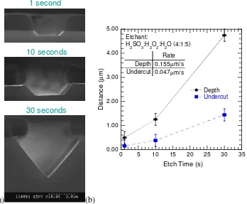
chemical etching from 1 s to 30 s. (b) A graph illustrating the total vertical etching depth (black line) and the resist under cutting with increasing etching time. ... 62 Figure 4.15. Schematics indicating (a) the die layout, (b) the rapid etch-depth vernier, (c)
the contact measurement test pads, and (d) the interdigitated metal grid fingers of the 1x1 cm2 device structures with grid finger spacing ranging from 490 µm to 40 µm. ... 64 Figure 4.16. Triple junction nipi-diode schematic indicating the various layers, doping
concentration, and thickness. ... 65 Figure 4.17. Effect of annealing on a nipi-diode with 90 µm grid finger spacing AM0
illuminated current vs. voltage characteristics... 66 Figure 4.18. Current vs. voltage characteristics for nipi-diodes with varying grid finger
separations; devices were excited with simulated AM0 illumination. ... 67 Figure 4.19. Short circuit current density dependence on nipi-diode grid finger
separation. ... 67 Figure 5.1. Schematic depicting the structure of an indirect-drive radioisotope battery. 70 Figure 5.2. Dieke diagram depicting the energy levels of trivalent lanthanide ions [86].73 Figure 5.3. Schematic of a D-A pair recombination center and a non-interaction D and A
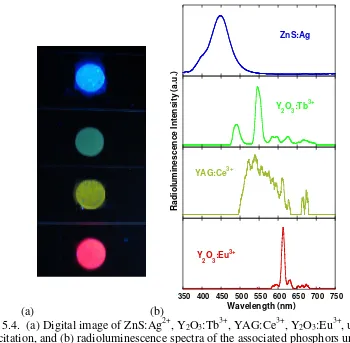
center... 75 Figure 5.4. (a) Digital image of ZnS:Ag2+, Y2O3:Tb3+, YAG:Ce3+, Y2O3:Eu3+, under 254
nm excitation, and (b) radioluminescence spectra of the associated phosphors under irradiation by a 0.1 mCi 210Po alpha-particle source. ... 76 Figure 5.5. (a) Schematic depicting the difference in energy of electronic states for
boxes of differing sizes, and (b) photoluminescence of CdSe QDs under 254 nm excitation. Reproduced with permission of Brian J. Landi [90]... 77 Figure 5.6. Energy level diagram depicting the possible energy level mapping schemes
photons while the upward facing arrows are emissions. Black wave-like arrows are symbolic of phonons. ... 78 Figure 5.7. Schematic depicting affects of film thickness on alpha-particle energy
absorption and self-absorption / scattering. ... 79 Figure 5.8. SEM images of Y2O3:Er3+ synthesized by the UREA precipitation technique.
Variable sizes were obtained by varying the EDTA concentration during
synthesis; the smallest particles had the largest concentration. ... 81 Figure 5.9. Alexandrite laser deposition reactor... 82 Figure 5.10. (a) Cross-sectional SEM image illustrating the undercutting obtained by
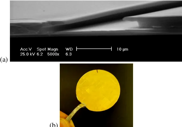
using LOR coated with SC-1813, and (b), digital image of a patterned 2-inch InGaP2/GaAs wafer after thermal deposition of top contact metal... 85 Figure 5.11. Test fixture/configuration for measuring the radioluminescent power output
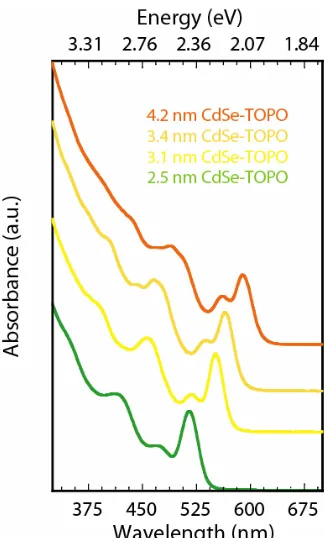
of the thin-film intermediate absorber layers deposited on quartz. ... 87 Figure 5.12. Optical absorption spectra for four different size distributions of
CdSe-TOPO QDs in a hexanes solution. Reprinted with permission by Brian J. Landi [90]... 88 Figure 5.13. Images of CdSe QDs under (a) ambient room light and (b) 254 nm
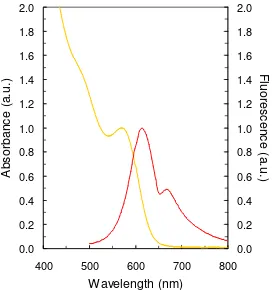
illumination with a UV lamp. (c) Fluorescence spectra for CdSe-TOPO QD samples in hexanes showing the size-dependent optical bandgap. Reprinted with permission of Brian J. Landi [90]. ... 89 Figure 5.14. Overlay of optical absorption and fluorescence spectra for the InP-myristic
acid sample in hexanes. Reproduced with permission of Annick Anctil [98]... 90 Figure 5.15. Fluorescence contour map (excitation vs. emission) of a 5% Tb3+ doped InP
(Myristic Acid-capped) QD sample synthesized at 270° C. The maroon lines are the result of the first order (slope = 1) and second order (slope = 2) reflections of the excitation source from the quartz cuvette. ... 92 Figure 5.16. Photoluminescence spectra for Y2O3:Eu3+,Ce3+ nanophosphor pre- and
post-anneal. The excitation wavelength was 488 nm. ... 93 Figure 5.17. Digital images of Y2O3:Eu3+, Ce3+ under (a) room light, (b) 254 nm
excitation, and (c) irradiation by a 210Po α-particle source... 93 Figure 5.18. Overlay depicting the spectral responsivity of an InGaP2 PV device and the
radioluminescence spectrum of a Y2O3:Eu3+, Ce3+ nanophosphor thin-film
irradiated by a 1 mCi 210Po alpha-particle source... 94 Figure 5.19. Y2O3:Eu3+ and Y2O3:Eu3+,Ce3+ radioluminescence emission spectra under
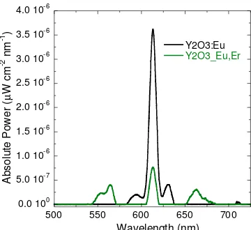
excitation by a 1 mCi 210Po alpha-particle source. ... 95 Figure 5.20. Y2O3:Eu3+ and Y2O3:Eu3+,Er3+ RL emission spectra under excitation by a 1
mCi 210Po alpha-particle source. ... 95 Figure 5.21. (a) Digital image of spray deposition apparatus, and (b) InGaP2 PV spectral
responsivity with respect to wavelength overlaid with the normalized
radioluminescence of Y2O3:Eu3+ (red curve) and Y2O3:Tb3+ (green curve) QD phosphors. ... 96 Figure 5.22. Representative thin-film QD phosphor profile measured using a Tencor
Figure 5.24. Peak radioluminescence emission from Y2O3:Tb3+ QD thin-films (550 nm) plotted with respect to the film thickness. ... 99 Figure 5.25. Normalized peak radioluminescence with respect to 4.2 MeV alpha-particle
fluence for Y2O3:Eu3+ (5%) with various particle sizes: 20-50 nm, 50-150 nm, 250-400 nm, and >500 nm. Solid lines represent linear curve fits and their
corresponding equations (correspond by color) are below the curves... 101 Figure 5.26. Normalized radioluminescence intensity as a function of alpha-particle
fluence for ZnS:Ag2+ and Y2O3:Eu3+... 102 Figure 5.27. Radioluminescence spectra of (a) YAG:Eu3+ and (b) YAG:Tb3+ under
excitation by a ~1 mCi 210Po alpha-particle source. ... 103 Figure 5.28. Normalized contour plot for a cross sectional ADEP within a QD film
comprised of nanocrystalline Y2O3 with a density of 3 g/cm3... 105 Figure 5.29. Digital photographs of a 1.0 cm2 InGaP2 PV cell (left), and a 0.25 cm2
InGaP2 PV cell (right) both have grid contacts with a center spike providing a 4% light shadowing... 106 Figure 5.30. (a) I-V response under simulated AM0 illumination and (b) spectral
responsivity for a representative InGaP2 photovoltaic cell... 107 Figure 5.31. Current density vs voltage plot for a prototype QD radioisotope battery
comprised of Y2O3:Eu3+ and an InGaP2 PV cell... 108 Figure 6.1. Dark diode current density vs. voltage for (a) 1QD and (b) 5QD, measured
over the temperature range of 100 – 400 K. ... 113 Figure 6.2. Spectral responsivity verses wavelength of over the temperature range of (a)
100 – 340 K for the 1QD device, and (b) 100 – 400 K for the 5QD device. In (c), the spectral responsivity of the 5QD device is plotted on a log-scale over the wavelength range of 800-1100 nm to better illustrate the InAs QD photogenerated current. ... 115 Figure 6.3. The (a) open circuit voltage, (b) short circuit density, (c) fill factor, and (d)
efficiency of the QDSC containing 1-layer of InAs QDs (QD1) and the QDSC containing 5-layers of InAs QDs (QD5) as a function of temperature. The lines in the figures are linear curve fits, the equations of which are included in the figures. ... 116 Figure 6.4. (a) Overlay of the pre-irradiated room temperature spectral responsivity of
the PIN (black circles), 1QD (blue squares), 5QD (red diamonds), with respect to wavelength. In (b), the spectral responsivity of the three devices post 6.7 × 10¹¹ alphas-particles/cm2 is plotted with respect to wavelength. ... 118 Figure 6.5. (a) The spectral responsivity at 830 nm as a function of alpha-particle fluence
for the PIN device (black circles), 1QD device (blue squares), and 5QD device (red diamonds), which corresponds to the GaAs bulk responsivity. (b) The
spectral responsivity at 900 nm as a function of alpha-particle fluence for the 1QD device (blue squares) and the 5QD device (red diamonds) which corresponds to the InAs QD responsivity... 119 Figure 6.6. (a) Diagram depicting the baseline GaAs solar cell and the strain
compensated QD solar cell structures. (b) Schematic depicting the energy bands of the strain compensated QD solar cell. ... 121 Figure 6.7. (a) Dark current-voltage response of baseline device and (b) the QDSC device
saturation currents as a function of temperature for the baseline device and the QDSC device, respectively. ... 123 Figure 6.8. (a) and (b) contain the current-voltage response of the baseline GaAs device
and the QDSC device, under simulated AM0 illumination, over the temperature range of 100 – 400 K, respectively. The summary data for these measurements are provided in part (c)... 124 Figure 6.9. (a) Spectral responsivity of the QDSC over the sub-GaAs bandgap range
depicting the variation in the InAs QD responsivity with temperature. For comparison, the 100 K and 420 K spectral responsivity of the baseline GaAs device have been overlaid as dashed and dot-dash lines and the location of the electroluminescence peak emission are included. (b) The variation in the
electroluminescence spectrum of the QDSC over the temperature ranging from 77 – 400 K... 125 Figure 6.10. Spectral responsivity spectra for (a) the baseline device and (b) the QDSC
device for various levels of alpha-particle fluence. ... 126 Figure 6.11. (a) Spectral responsivity of the QDSC at incremental levels of alpha-particle
fluence; the pre-irradiation and post 3.5 x 10¹² alpha-particle/cm2 responsivity spectra of the baseline device are overlaid for comparison. (b) The spectral responsivity as a function of fluence measured at 830 nm for both devices and at 910 nm for the QDSC. ... 128 Figure 6.12. Normalized short circuit current, open circuit voltage, fill factor, and
efficiency with alpha-particle fluence for the baseline and the QDSC devices.. 129 Figure 6.13. (a) Zinc blend bonding structure of InAs, where In and As atoms are
represented by blue and red spheres, respectively. (b)-(f) Depictions of the simulation process where an In (As) is displaced from its equilibrium bonding sight into points locations within the lattice. At each displacement, the potential energy of the atom is calculated... 131 Figure 6.14. Equi-potential surfaces indicating the locations of local minima for As
within the InAs lattice. Moving from left to right, the four blue spheres correspond approximately with the following crystal locations (x,y,z) =
(a/4,3a/4,a/4), (a/4,a/4,3a/4), (3a/4,3a/4,3a/4), and (3a/4,a/4,a/4). The surface near (0,0,0) corresponds to the top of the well (in energy) that the atom sits when in its equilibrium position. An In atom is located at (a/4,a/4,a/4) and therefore these four interstitial sites surround that atom. ... 132 Figure 6.15. Potential energy of an Indium PKO along r = (201) for a relaxed InAs
lattice (black trace) and a strained lattice (green trace). ... 133 Figure 6.16. Effect of strain on the equilibrium lattice cohesive energy of the atom.... 134 Figure 6.17. Effect of strain on the minimum knock-out energy required to reach the
labeled interstitial sites for (a) In and (b) As as the PKO. ... 135 Figure 6.18. Contour map depicting the log of the minimum energy for displacement
along direction (φ, θ) for an In PKO in relaxed InAs. ... 137 Figure 6.19. Contour map depicting the log of the minimum energy for displacement
LIST OF TABLE CAPTIONS
CHAPTER 1.
INTRODUCTION
The accelerated development of microelectronics coupled with improved bulk and
surface micromachining techniques have enabled the growth of economically feasible
and highly functional microsystems [1]. Blanchard and Fabrycky define a system as “…a
set of interrelated components working together toward some common objective or
purpose” [2]. Therefore, a microsystem may be defined as a set of interrelated
components on the sub-millimeter scale working together toward some common
objective or purpose. Such “common objectives” may be accomplished, for example, by
integrating one or many optical switches, pressure sensors, fluid valves, inertial sensors,
etc., together with microprocessing and telemetry subcomponents [1, 3]. The net result is
an integrated system with increased functionality and concomitant low power
consumption, mass, and size.
To date, microsystems have been dominated by Si electronics and sensors;
however, the integration of III-V based components could potentially extend the utility of
microsystems to the expanding fields of high frequency communications along with a
wide host of optoelectronic based technologies. For instance, the high electron mobility
and velocity saturation limit in GaAs and InP have made them ideal for high-frequency
and high-power satellite communications [4, 5]. III-V semiconductors are the basis of
advanced multi-junction photovoltaics [6], which are the current standard for space
power generation systems. Furthermore, III-V semiconductors are widely utilized in
infrared sensing, light emitting diode, and lasing applications [7]. An additional class of
materials which can expand the functionality of microsystems is nanomaterials. The
properties, and the ability to functionally integrate them within existing III-V based
devices.
The main applications requiring the advantages offered by microsystems are often
associated with remote or harsh environments in which data cannot be easily extracted
without extensive infrastructure. Remote locations including desert, oceanic, and
mountainous regions can all be characterized as having constantly changing temperature,
pressure, humidity, etc., which can effect the operation of microsystems. When
employed in space satellite applications, the devices are repeatedly thermally cycled as
the satellite moves into and out of eclipse. There are many terrestrial and space
applications in which some or all of the microsystem’s components are exposed to
ionizing radiation. Ionizing radiation, including gamma rays and high-energy charged
particles, can lead to failure in semiconductor-based electronic device due to rapid
ionization events, or cause a slow continuous degradation in the performance of
electronic devices resulting from trapped charges and a reduction in minority carrier
lifetimes [8, 9].
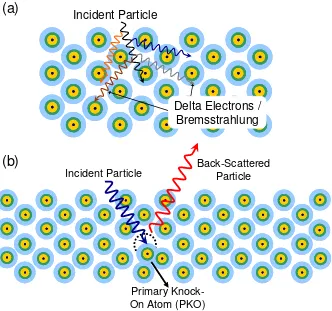
The schematic in Figure 1.1a, is a simplified depiction of an atomic ionization
process where an incident high energy particle loses energy through interactions with the
electrons encountered while traversing through a material. This form of energy loss
accounts for >99% of the energy loss of charged particles (i.e., partially or fully ionized
atoms) and likewise for electrons with energies < 0.5 MeV [10, 11]. These primary
collisions create forward scattered electrons within the semiconductor, which
the case of transistors, the large field present can result in a dangerous current spike
potentially leading to a damaging latch-up condition [9]. However, this process is not in
all cases disadvantageous. In fact, it is the fundamental operating mechanism used in the
detection of nuclear radiation from unstable elemental isotopes in gas-filled counters and
semiconductor junctions; it is also the mechanism which allows smoke detectors to sense
small amounts of smoke within the nearby environment [10, 12]. The ionization of
atoms and generation of excited charge carriers is analogous to creating electron-hole
pairs in a photovoltaic device excited by light. Therefore, with a properly designed
semiconductor device structure, it is possible to capitalize on this form of radiant energy
transfer and use it to generate power [13]. A better understanding of the interaction
between ionizing radiation and nanomaterials or III-V devices will be critical to the
development of novel materials and devices which can enhance the sensing or power
Incident Particle Back-Scattered Particle
Primary Knock-On Atom (PKO) Incident Particle
Delta Electrons / Bremsstrahlung
(a)
(b)
Figure 1.1 (a) Schematic depicting the loss of energy by an incident particle either through collisions with valence and core electrons or through Bremsstrahlung radiation which will be discussed in Chapter 2. (b) Schematic depicting the displacement of a lattice atom as a result of an incident particle collision. The trajectories of the Primary Knock-On (PKO) atom and the back-scattered particle are indicated.
The primary cause for the slow continuous degradation observed in the
performance of semiconductor-based electronic devices is schematically depicted in
Figure 1.1b. In this schematic, a high-energy particle is incident with, and transfers some
or all of its energy to, a bonded atom within the semiconductor lattice causing it to
become displaced. Following the collision, the primary knock-on (PKO) atom traverses
the material, losing energy through electronic and nuclear collisions. Along the path of
the PKO is a column of vacancies and near-by atoms occupying interstitial sites which
[image:19.612.160.492.76.387.2]degradation in the device performance to be observed. Characteristic degradation
equations, parameterized based on empirical data, are often used to describe the variation
in the device performance with increasing defects [14-19]. Such equations have been
shown to adequately describe the variation in III-V based photovoltaic devices under
exposure to high-energy photon, electron, neutron, protons and other light charged
particles. However, to better understand the degradation mechanisms, and to design new
structures for reducing the rate of damage, a more fundamental investigation is necessary.
Such information can then be utilized to increase the lifetime of microsystems employing
III-V bulk and quantum confined semiconductors whether exposure is intentional, as in
radioisotope power generation devices, or is an incidental result of the environment in
which the system is utilized.
The organization of this dissertation is as follows, Chapter 2 contains background
information on fundamental ionizing radiation – matter interactions and a historical
review of solid state radioisotope batteries. Additionally, an overview of nanomaterials
with an emphasis on epitaxially grown InAs quantum dots, and the use of these materials
in GaAs solar cells is provided. To accomplish the goal of understanding the effects of
ionizing radiation on nanomaterials and III-V semiconductor devices, a series of
theoretical and experimental investigations have been conducted. The main experimental
“tool” for this research is a 210Po radioisotope source that emits ~ 5.4 MeV alpha
particles. Such particles have a high rate of ionizing energy loss and are energetic
enough to cause lattice dislocations. Theoretical models (referred to as ADEP and D3P)
are developed in Chapter 3 to understand how the alpha-particle flux emitted from an
generating) energy into a material. Also in Chapter 3 is an overview of a modeling
approach developed to investigate the vacancy generation process in III-V
semiconductors. This is accomplished by a molecular dynamics modeling approach for
calculating the minimum energy necessary to create a lattice defect. Chapters 4-6 are
applications of the theoretical and experiential results provided in the early chapters.
Chapter 4 provides experimental validation for the ADEP modeling procedure and
highlights the experimental and theoretical development of direct conversion radioisotope
batteries. Chapter 5 pertains to the development of indirect conversion radioisotope
batteries with an emphasis on the development of nanophosphor materials. In Chapter 6,
the D3P model and molecular dynamics model are utilized to investigate the effects of
non-ionizing radiation on III-V-based solar cells in which nanomaterials are incorporated.
Chapter 7 concludes this dissertation with a summary of the key findings and how they
CHAPTER 2.
BACKGROUND INFORMATION
2.1
R
ADIATIONI
NTERACTIONS WITHM
ATTERRadioactive isotopes, or radioisotopes for short, are elemental isotopes whose
nuclei are unstable due to a lack or surplus of neutrons. This instability results in
spontaneous nuclear decays which may be in the form of beta particles, alpha particles, or
gamma rays. These decays are a primary source of radiation exposure for electronic
devices employed in terrestrial applications. The rate at which a radioisotope decays is
proportional to the number of radionuclides, N, present and the probability of decay,λλλλ:
N dt
dN
λ λ λ λ
−
= . (2.1)
Using the activity,Ao ≡ Noλλλλ, where No is the initial number of radionuclides, the activity of a radioisotope sample as a function of time is given by:
A= Aoexp
(
−λλλλt)
(2.2) A commonly used unit of activity is the curie (Ci) which is equal to 37 billondecays per second. The parameter used to characterize the life time of a radioisotope is
its half-life, t1/2 =ln
( )
2 λλλλ, which corresponds to the time it takes half of a given sample to decay.A beta particle is a high energy electron created at the moment of neutron decay
and emitted from the nucleus of the radioisotope. A portion of the energy lost in the
neutron decay may also be imparted to a second subatomic particle called an antineutrino.
Antineutrinos are neutral particles which weakly interact with matter and therefore their
effect on matter is commonly ignored. The division of energy between the two particles
from nearly zero to a radionuclide-specific maximum energy. The maximum energy of a
single beta particle emission equals the difference in rest energies between the parent and
daughter atom (Eβ,max = mpc2 – mdc2 - mec2). In order to conserve momentum, most of this energy is imparted to the beta particle since its mass is much smaller than that of the
nucleus. Obeying the law of conservation of electric charge the previously neutral
neutron takes on a positive charge thereby forming a proton which leaves the daughter
atom with an atomic number one greater than the parent. For some radioisotopes, the
maximum energy of the emitted beta particle can exceed 1 MeV, however most
maximum energy emissions are <500 keV.
An alpha particle is a high energy particle emitted from the nucleus of a
radioisotope and consists of two protons and two neutrons (a double ionized helium
atom). The energy of the emission is approximately equal to the rest energy of the parent
atom minus the rest energies of both the daughter atom and the alpha particle. Again,
most of this energy is imparted to the alpha particle because of the disparity in masses.
As a result, the energy per alpha-particle decay for a given radioisotope is nearly
constant; however, depending on the angular momentum of the emitted particle, different
emission energies may result. The remaining energy is conserved by leaving the nucleus
of the daughter atom in an excited energy state. An alpha decay results in a daughter
atom which has an atomic number that is reduced by two and an atomic weight that is
reduced by four. Most common alpha particle emissions energies range from 3 MeV to
7.5 MeV.
occur spontaneously or in conjunction with beta and alpha radiation. Gamma rays result
from energetic transitions of nuclei which have been left in an excited state after
undergoing a radioactive decay, or as the result of a violent collision with another
particle. They consist of extremely energetic emissions of electromagnetic radiation
which can range from a few keV to hundreds of MeV.
An analysis of the interaction with matter for the different types of radioactive
decay is necessary when considering each for power generation. Alpha and beta particles
both carry charge and therefore interact Coulombically with the electrons and nuclei of
the material traversed. The diameter of an atom is on the order of 10-10 m while the
nuclear diameter is about 10-15 m. With 1015 times more volume occupied by electrons,
elastic and inelastic electronic collisions with alpha and beta particles are much more
probable making this the primary form of energy loss. Beta particles may also dissipate
energy in the form of bremsstrahlung radiation which is the emission of light due to the
(de-) acceleration of electrons in the electric field of the nucleus. The total rate of energy
loss of the beta particle as it traverses matter is the sum of the Coulombic and radiative
losses [13]: rad c dx dE dx dE dx dE + = (2.3)
Accounting for relativistic velocities, the Coulombic and radiative energy loss portions
can be modeled by [10]:
and
(
)
(
)
(2.5)3 4 2 ln 4 137 4 2 2 4 2 2 2 0 2 − + + = c m c m T c m c m T N Z e dx dE
rad ππππεεεε
where e is the electronic charge, Z is the atomic number of the absorber, N is the atomic
density of the absorber, m is the electron rest mass, v=ββββcis the velocity of the particle,
c is the speed of light, T is the kinetic energy of the particle, I is the mean excitation
energy of the atomic electrons, and εεεε0is the permittivity of free space. Equation (4)
indicates that the rate of energy loss due to Coulombic interactions increases with
decreasing particle velocity. It is also greater in materials with higher densities. The
relative contributions of the two terms can be found by their ratios which is
approximately: 1600 2 2 Z c m c m T dx dE dx dE c
rad = +
(2.6)
This proportion shows that the radiative term is significant only at high energy and in
heavy materials. In most semiconductor diodes (e.g., Z ~ 28 for InGaP2) the radiative
contribution is less than 2% for T < 100 keV.
A similar expression to (4) can be used to give the magnitude of the energy loss of
alpha particles per unit length due to Coulombic interactions:
(
)
− − + = 2 2 2 2
2 2 2 2 0 2 1 ln 2 ln 4
4
β
β
β
β
β
β
β
β
β
β
β
β
β
β
β
β
π
π
π
π
εεεε
π
π
π
π
I c m c m N Z z e dx dE c (2.7)for relativistic velocities and can be ignored for alpha particles with energies <10 MeV.
For alpha-particles, the range of the particle can be found by integrating the inverse of the
rate of energy loss with respect to the energy of the particle, and has been shown to
provide similar results to those obtained experimentally. In contrast, the large degree of
scattering for beta particles necessitates the use of an empirical relationship when
determining their range in matter [10].
Gamma rays interact with matter primarily through three processes: photoelectric
absorption, Compton scattering, and electron-positron pair production. In the
photoelectric effect, an atom absorbs the gamma ray and an atomic electron
(photoelectron) is released. The energy of the emitted photoelectron is equal to the
kinetic energy of the gamma ray less the binding energy of the electron. The probability
of photoelectric absorption is significant only for lower energy photons (<100 keV) and
increases for materials with higher atomic numbers [10]. Compton scattering is the
process by which a photon scatters from a nearly free electron resulting in a less energetic
photon and a scattered electron that carries the energy lost by the photon. This process is
more probable for lower energy photons and in materials which have greater free electron
densities (e.g., Pb). In an electron-positron pair production process, the photon is
annihilated causing all of its energy to be given to the two particles and its probability is
significant for gamma rays with energies exceeding 5 MeV.
The total linear attenuation coefficient,µµµµ, is used to describe the rate of photon
(gamma ray) removal for a given thickness of material. The linear attenuation coefficient
and pair production. Thus, the intensity of gamma rays after passing through an absorber
with thickness, t, with an initial intensity, Io, is:
) exp( t I
I = o −µµµµ . (2.8)
This equation is useful when determining the necessary shielding required to adequately
attenuate the unwanted gamma rays associated with alpha- or beta-particle decay. The
linear attenuation factors have been used to determine the specific gamma-ray dose
constants for nearly all radionuclides by Oak Ridge National Laboratory [20].
The linear energy transfer of both alpha and beta particles is far greater than that
of gamma particles thereby making the effective range of these particles much shorter.
Additionally, the primary form of energy transfer of both alpha- and beta-particles is by
electronic collisions thereby directly resulting in the formation of electron-hole pairs in
semiconducting materials. The greater mass of the alpha particles, as compared to beta
particles, and larger charge causes it to dissipate energy many times faster than beta
particles. As a result, the maximum range in H2O is approximately 50 µm for a 5 MeV
alpha particle and it is approximately 2 cm for 5 MeV beta particles (200 µm for a 100
keV beta particle). Alpha-particles, therefore, are more attractive for power generation
devices because less material is required to completely stop the particle. The long range
and various modes of energy deposition make gamma particles the least attractive
radioactive emission. However, it is still important to investigate the gamma emissions
2.2
S
OLIDS
TATER
ADIOISOTOPEB
ATTERIESSolid state radioisotope batteries are devices which utilize a semiconductor p/n
junction to convert the radiant energy of a radioisotope into electricity. These devices
may be categorized into two classes, a direct conversion radioisotope battery and an
indirect conversion radioisotope battery. The former directly converts the kinetic energy
of the sub-atomic particles emitted from a radioisotope into power in an analogous
manner as that of a photovoltaic diode converting light into power. Indirect conversion
devices make use of a two-stage energy conversion process whereby the radiant energy
from the radioisotope is converted to light by a radioluminescent phosphor, the light from
which is subsequently converted into electricity via a photovoltaic diode.
The concept of utilizing a solid state device to generate power dates back to 1951
when Ehrenberg et al. first demonstrated the so-called electron voltaic effect [21]. Also
in that year, McKay et al.,reported the generation of electron hole pairs by
alpha-particles [22]. In this report, a commonly used empirical formula was developed relating
the energy required to create an electron hole pair Epair, to that of the semiconductor
bandgap Eg namely: Epair – Eg = 3 ±0.4 [eV]. A second empirical result was also
discussed in this report which was Epair = ~3Eg/2 [eV], though this relationship was only
valid in a few materials investigated.
There are three “efficiency” metrics which will be used to evaluate the
performance of radioisotope batteries. The overall efficiency, ηtot = Pe/Pn is referred to as
the nuclear-to-electrical efficiency. This is a ratio between the electrical power output of
the device Pe and the nuclear power emitted from the radioisotope source Pn. This
will be the primary metric used to compare the different radioisotope batteries reported in
the literature, is the semiconductor conversion efficiency ηsemi = Pe/Pn,semi which is the
ratio of the output power to the nuclear power incident with the semiconductor device.
This corrects ηtot to account for less-than-ideal coupling between the radiation source and
the semiconductor device due to poor geometry matching. Poor geometry can be
overcome by directly depositing the radioisotope source onto the semiconductor device;
however, for conducting research it is more efficient to utilize a single radioisotope
source, deposited onto a foil substrate, for measuring the efficiency of different devices
and structures. The final efficiency metric ηx where x = α or β is similar to a quantum
efficiency value and is defined as the ratio between the number of charge carriers
extracted by the device and the total energy of the incident particle (in eV-1).
The first betavoltaic battery study was performed by Rappaport [23], in 1954, and
later that same year by Pfann and Van Roosbroeck [24] (see Figure 2.1). In both of these
studies, sources comprised of 90S - 90Y were used to excite Si and Ge p/n junctions
fabricated by thermal dopant diffusion. The wider bandgap, and correspondingly lower
intrinsic carrier concentration and dark current, allowed the Si devices in both reports to
generate nearly an order of magnitude more power than that of the Ge devices. The
lower power output of the devices reported by Pfann et al., is due to a shield that was
used to reduce the flux of high energy beta particles which had recently been shown to
cause damage in Si and Ge semiconductor materials [23]. In 1965, the first alphavoltaic
battery research was reported wherein an alpha-particle source was coupled to both Si
damage caused a significant drop in the power output, although the GaAs device
withstood nearly an order or magnitude more fluence before degrading by the same
extent [25].
A major breakthrough in betavoltaic technologies was the development of high
purity promethium-147 radioisotope source. 147Pm is a soft-beta emitter (βmax ~250 keV)
and therefore is relatively benign to the semiconductor converters [26]. In 1964, Flicker
et al. reported their 2-year study on a 147Pm:Si betavoltaic battery which demonstrated a
beginning-of-life power output of 9.1 µW/cm2 and degraded with a half life only slightly
shorter than that of the 147Pm source itself (t
1/2 = 2.6 years for 147Pm). It was suggested
that trace amounts of 241Am could have been present which emits 5.5 MeV
alpha-particles. The ηsemi for this device was 1.5% and it consisted of a 2π geometry and a total
radioisotope source loading of 6.8 Ci. A 2π geometry means that only half of the radiant
energy from the source is converted by the device; a 4π geometry utilizes the radiate
energy emitted from both sides of a thin film radioisotope source material by
sandwiching it between two semiconductors which are serially or parallelly connected
depending on whether high voltage or high current is desired, respectively. A device
with a 4π geometry was also tested by Flicker and co-workers but the performance
suffered due to poor current matching through the serially connected stack and therefore
had an efficiency of only 0.4% [26]. Barnes et al., reported on a 147Pm:Si betavoltaic
battery with a 4π geometry which demonstrated a 10 µW/cm2 peak power output with an
ηsemi of ~2% and a source loading of 4 Ci [27]. Olsen further improved upon this
technology and demonstrated a promethium based betavoltaic battery which output 23
battery to power implantable cardiac pacemakers. Many different radioisotope battery
technologies, including direct conversion, direct charge, and thermoelectric devices, have
been considered (and some have been tested) as long life pacemaker batteries; a good
review of these technologies is provided by Huffman etal. in ref. [29].
Figure 2.1, referred to earlier, contains a timeline of the radioisotope devices
reported in the literature since 1951. The rectangles indicate the semiconductor material,
radioisotope source used, and the geometry of the device, i.e., 2π vs. 4π. Down the
center column is a chart depicting the power output (in log-scale) of the devices and the
year in which they were reported. The markers on the chart are color coded to
correspond with the device and the numbers on the marker indicate the reported (or
calculated) ηsemi. In most instances, the ηsemi was not provided and was calculated based
on the data provided in the manuscripts. Therefore, the power and efficiency values
plotted in Figure 2.1 are accurate to ~15% relative (based on one’s ability to extract data
from graphs visually). There is a large gap in time, extending from the mid 1970s into
the early 1990s, during which no reports on radioisotope batteries appear in the literature.
Interestingly, the dates of the partial melt-down at the nuclear power generation station
on Three Mile Island in Pennsylvania (1979) and the nuclear power generation station
explosion in Chernobyl Ukraine (1986), the worst nuclear disaster in world history,
occurred during this time period.
In the early 1990s the first demonstration of a radioluminescent light source
coupled to a semiconductor diode was reported [30]. The novelty of this approach is the
radioisotope source into light. In 1994 Sims et al., reported the results of simulated
indirect conversion radioisotope devices using a GaP solar cell (Eg=2.26 eV) excited by a
sealed ZnS:Ag / Tritium (3H) light source [31]. The electron-to-light conversion
efficiency of the phosphor was reported as 20.1% and the conversion efficiency of 6%
was achieved by the GaP device under the low intensity ZnS:Ag light emission, which
peaks at 450 nm. This device had good stability, but due to the low energy beta particles,
self absorption was an issue limiting the power to 550 nW/cm2.
In the mid 1990s Kosteski and co-workers reported their research on using 3H to
replace the H atoms typically used in amorphous Si to passivate the dangling Si bonds at
grain boundaries [32]. Deus et al., demonstrated an amorphous Si device with improved
power output, and he, along with Andreev et al., showed great improvements in power
output, efficiency, and longevity, by employing a 3H radioisotope source with a III-V
semiconductor converter [33, 34]. The III-V device was comprised of AlGaAs, which is
a wide bandgap material ranging between 1.4 eV – 2.2 eV depending on the
concentration of Al. Deus’s 3H:AlGaAs device achieved a maximum power output of
259 nW/cm2 with an efficiency of 2.3%. The device reported by Andreev et al. had
comparable efficiencies under similar 3H activity, though to increase the power output by
a factor of 2 over that of device reported by Deus et al., the 3H loading had to be
significantly increased. This large increase in loading was necessitated by the self
shielding effects of the low energy beta particles emitted from 3H. The AlGaAs material
improved the efficiency greatly because the large bandgap increases the shunt resistance
allowing for an open circuit voltage of ~0.9 V to be achieved with a generated current of
In 1996, Rybicki et al., was the first to report on an alphavoltaic battery
comprised of the newly developing SiC semiconductor material with a bandgap between
2.3-3.3 eV depending on the morphology. This device had a bandgap of 3 eV, generated
14 nW/cm2 with a η
semi of 3.1% and ηα of 18% [35]. The low power output of the device was a consequence of the low activity 241Am source; when tested at higher fluxes the
increased power output was concomitant with a rapid rate of degradation. Fleurial et al.
investigated an alphavoltaic battery employing 244Cm and a GaAs diode. The device
achieved a power output of 90 µW/cm2 but this quickly degraded to 10 µW/cm2 in only
10 minutes of operation [36]. In 2006, Cress et al., demonstrated 50.6 nW/cm2 with a 1
mCi 210Po source coupled with an InGaP2 p/n diode. The device had a ηsemi of 3.2%, a ηα of 36% and had a half life of about 30 days [37]. This ηα value was consistent with the maximum monochromatic spectral responsivity measured for that device and was
calculated using the ADEP modeling procedure which is discussed in Chapter 3 [38].
Increases in the efficiency were observed in betavoltaic devices employing soft
beta particle sources, such as 3H and 63Ni, but suffer from self absorption because the
energy of the emitted beta particles is insufficient for beta particles within the material to
escape. Consequently, the maximum power output that can be achieved with these
sources is severely limited. To mitigate these effects, novel techniques have been used to
increase the active surface area of the semiconductor junction thereby maximizing the
incident flux. Guo et al. fabricated inverted pyramids into a Si wafer and subsequently
processed the wafer to form a p/n junction across the entire structured surface. The
liquid source solution [39]. With similar intentions, a 3D p/n diode fabricated from
porous silicon was measured under 3H irradiation [40]. This device only generated 0.17
nW/cm2 with a ηsemi of 0.2%; however, the ratio of the power generated within the pores
to that of the power generated from the surface resulted in a 9x efficiency improvement.
In 2006, the use of soft-beta emitters, 63Ni and 33P used in conjunction with wide
bandgap SiC diodes were investigated by Chandrashekhar, et al.[41], and Eiting, et al.
[42], respectively. In the former, a SiC was excited by a 1 mCi 63Ni source as well as by
a scanning electron microscope (SEM) operated at ~17.5 kV (to simulate the average beta
particle flux). This device is reported to have exceptionally high efficiency, ηsemi = 6.3%,
although the size of the device was only 2.5 mm2. Moreover, the SEM-simulated beta
particle flux will inflate the efficiency obtained because all of the electrons are normally
incident with the diode and will stop very close to the surface. In a real betavoltaic, the
higher energy betas (i.e., Emax = 65 keV for 63Ni) would penetrate much deeper into the
device leading to less efficient conversion. The device reported by Eiting consisted of a
SiC diode excited by a 225 mCi 33P source which had very good efficiency, ηsemi = 4.5%,
and power output 2 µW/cm2 however the 33P has a half life of 25 days making this
1960
1970
1990
2000
1951 Ehrenberg, et al.1954- 56 Rappaport et al.
GaAs α α α α AlGaAs 3H Si 147Pm
10
-910
-710
-5Power (W/cm
2)
Si
90Sr -90Y
Ge
90Sr -90Y
1954 Pfann, et al.
Si
90Sr -90Y
Ge
90Sr -90Y
1964 Flicker, et al. Electron Voltaic Effect
Si α α α α InGaP 210Po 1965 Posey
1965 Barnes, et al.
<1%
Si
147Pm
Si
1972 - 1974 Olsen
Si 147Pm GaP 3H SiC 241Am
1991 Walko, et al.
1996 Rybicki, et al.
GaP
3H
1994 Sims, et al.
2006 Cress, et al.
3D-Si
3H
2005 Sun, et al.
α αα α-Si 3H α αα α-Si 3H
1996 Kosteski et al.
2000 Andreev, et al.
3D-Si
3H
2003 Guo, et al.
*2006 Chandrashekhar, et al.
SiC
33P
2006 Eiting, et al.
SiC
63Ni
AlGaAs
3H
2000 Deus, et al.
1951 McKay
e-& h+Production Alpha
Si 147Pm Si 0.2 0.36 4.5 3.1 GaAs 244Cm
2001 Fleurial, et al.
ZnS:Ag
Three Mile Island (1979)
Chernobyl (1986) 0.8 6.2 3.2 ~2 1.5 0.4 ~2 0.5 0.8 2.4 1.2 0.1
*Simulated 63Ni with SEM
© 2008 Cory D. Cress
0.4 3.5
[image:35.612.111.541.71.633.2]20.1 6.3
Based on this review of betavoltaic and alphavoltaic batteries, many conclusions
may be drawn. The low current level of radioisotope batteries makes the shunt resistance
the critical diode quality parameter, which is in contrast to photovoltaic applications
where currents are high and therefore necessitate low series resistances. This in addition
to low saturation currents and high diffusion lengths are the critical parameters for
achieving high efficiencies at low levels of excitation. These requirements can all be met
by using a wide bandgap semiconductor diode; the high efficiencies obtained by the
AlGaAs, InGaP2, and SiC devices provide experimental evidence supporting this
conjecture (see Figure 2.1). Employing these materials in conjunction with 3-D device
structures may prove effective at increasing the efficiencies further.
The choice of radioisotope is as important as the semiconductor diode utilized.
The energy density, activity density, half life, emission energy, and decay type must all
be considered. The transition from 90Sr – 90Y to the soft beta emitter, 147Pm, had a
profound effect on device performance including increased efficiency and lifetime.
However this material is not favorable for long-term power supplies because the half life
is only 2.6 years. 63Ni and 3H are both soft beta emitters (maximum beta particle energy
is ~65 keV and ~19 keV, respectively), and have half lives in excess of 10 years. As
observed in Figure 2.1, the low energy of these beta particles causes self absorption to
become a problem. In fact the maximum power emitted per unit area of 3H gas is
14 µW/cm2 and only 0.21 µW/cm2 from 63Ni [13]. This is because the added material
shields as many beta particles as it contributes. The modern devices employing
alpha-particle irradiation all achieved good ηsemi values because the alpha particles have a
damage caused by alpha-particles is a major impediment. Based on simple conservation
of momentum and energy arguments, the energy needed by an alpha-particle to cause a
lattice displacement is about 4000 times less than that required by an electron [10]. To
generate a defect in GaAs, a 225 keV beta-particle is needed [26]. This means that a
57 eV alpha-particle would have sufficient energy to generate defects in this material.
Before alpha-particle emitters can be successfully utilized in direct conversion or indirect
conversion radioisotope batteries, it is necessary for major developments in
radiation-tolerant materials to be performed. However, the use of alpha-particle sources as an
experimental tool is very useful for understanding the operation of novel device
structures or materials, and to investigate the damaging effects of ionizing radiation.
2.3
N
ANOMATERIALS ANDN
ANO-E
NHANCEDD
EVICESA nanomaterial can be broadly defined as a material which has at least one
dimension that is measurable on the nanometer scale. With this broad definition, the
components (i.e., gate oxides, gate electrode, source-drain metal contacts, etc.,)
comprised in integrated circuits from as far back as the 1990s could all be considered
nanomaterials. However, there is nothing truly special with the materials used in these
devices when compared with the properties of their corresponding bulk materials.
Therefore, perhaps erroneously, the buzz words “nanomaterial” and “nanotechnology”
imply that the size of these materials is the unique aspect of interest. In contrast, the
interest in nanomaterials is based upon the unique and potentially tunable properties
which can be obtained in certain materials when their size is reduced to the nanometer
Generally speaking, unique properties that have been observed in nanomaterials
include improved catalytic behavior, enhanced plasmonic absorption, increased or
decreased optical absorption, enhanced magnetic properties, and the list goes on [43].
The existence of these unique properties may be attributed to several factors including
[44]:
● The surface atom to interior atom ratio is on the order of one.
● The ratio of the surface energy to the total cohesive energy is on the order of one.
● The conduction and valence electrons are confined to small length or volume and
therefore the minimum wavevector is longer than in the bulk.
● The observed increases in strength among nanometal clusters results from the
difficulty to move dislocations in spatially confined regions.
Many of these properties are only observable at the nanometer scale and are not
necessarily tunable. However, in III-V and other semiconductor systems, as the
dimension of these materials becomes reduced, quantum size effects become apparent. In
particular, the optical and electronic bandgap can be increased to many times the bulk
bandgap depending on the fundamental materials properties and on the dimensionality of
the size reduction. Such size dependent properties are typically referred to as quantum
size effects and result from confinement of the electron motion within the lattice in one,
two, or three dimensions.
Figure 2.2 is useful for illustrating the fundamental origination of quantum
confinement (quantum size effects) in one, two, and three dimensions. On the left
column of this figure are schematics depicting a bulk structure, a quantum well, quantum
a periodic crystalline lattice. The periodicity makes it useful to mathematically describe
the lattice in reciprocal space thereby making Fourier analysis straightforward. Like the
lattice, the propagation of an electron in the lattice can also be described in reciprocal
space and is referred to as the wavevector k =2ππππ λλλλ
r
, where λ is the wavelength of the
electron. This transformation results in possible k
r
ranging from 0 to ~2π/a, where a is
the lattice spacing, as opposed to using wavelengths which range from ~0 to infinity [44].
As the dimensionality of the semiconductor crystals is constricted, the set of allowable k
r
become reduced, starting with a reduction in short k
r
which correspond to long
wavelengths. The schematics in the center column of Figure 2.2 illustrate how the
allowable k
r
states (in the conduction band) become reduced with 1, 2, and 3
kx ky kz
kx ky
kz
∆kz~1/dz
kx ky
kz
∆kz~1/dz
∆ky~1/dy
kx ky
kz
∆ky~1/dz
∆kx~1/dx
∆ky~1/dy
[image:40.612.129.522.72.443.2]Bulk Quantum Well Quantum Wires Quantum Dots D O S 0-D Confinement Energy D O S 1-D Confinement Energy D O S 2-D Confinement Energy D O S 3-D Confinement Energy
Figure 2.2. Moving from left to right the schematics depict the structure under consideration, the corresponding allowed electronic k
r
in reciprocal space, and the density of states with respect to energy for electrons referenced from the top of the valence band. Increasing confinement is depicted from the top down beginning with no confinement, 1-D, 2-D, and 3-D.
The final column of this schematic depicts the resulting density of states (DOS) in
the conduction band (after zone folding [44]) for the materials with the various
dimensionalities of size confinement. The density of states is the number of states
between Ekr and k
Er+ k
dEr. These relationships are determined by differentiating the
total number of states up to energy Ekr with respect to energy, where k
Er is related to k r
by 2*
(
2 2 2)
2 x y z
e g
k k k k
m E
Er = + h + + and E
DOS is obtained from the allowed k
r
requires the use of an example. Consider a sphere
centered at the origin on the reciprocal space state map for the bulk material in the figure
above (the sphere having a radius of k = kx2+k2y +kz2
r
). For a very small sphere, there
are no states present indicating a bandgap; as the sphere increases in size, the number of
states increases. The DOS of states corresponds to the rate of change in the number of
states which are within this sphere1. In the case of the quantum well the density of states
follows analogously; however, one degree of freedom has been lost so the states fill a
circle in k
r
-space. The rate of change in the number o