International Journal of
ELECTROCHEMICAL
SCIENCE
www.electrochemsci.org
A Facile Strategy for the Growth of an Anodic Oxidation Film
of the Ti13Nb13Zr Alloy Driven by Residual Stress
Wei Wang1, Yan Lin1, Yuan Wang1,*, Xiaohua Yu2,*, Ju Rong2, Yannan Zhang2, Jing Feng2
1 School of Machinery and Manufacturing Engineering, Southwest Forestry University, Kunming
650224,China
2 National Engineering Research Center of Solid Waste Resource, Kunming University of Science and
Technology, Kunming 650093, China
*E-mail: [email protected], [email protected]
Received: 9 October 2018/ Accepted: 10 January 2019 / Published: 7 February 2019
Anodizing offers a promising solution to improve the corrosion resistance of Ti and Ti alloys; however, the development of dense and thick anodic oxidation films remains an important scientific problem. Herein, we report a novel and facile strategy for the growth of an anodic oxidation film of the Ti13Nb13Zr alloy driven by residual stress. Under residual stress conditions, the gradient defect film on the Ti13Nb13Zr alloy surface is prepared. The change is coupled to an increase in surface defects and the surface Gibbs free energy, providing structural disorder and boosting the intrinsic activity of the Ti13Nb13Zr alloy surface, which strongly enhances the compactness, thickness and corrosion resistance of the Ti13Nb13Zr surface anodic oxide film. The thickness of the oxide layer increases up to 47.1% under the best residual stress condition. Furthermore, the donor density reduces by 500%, the self-corrosion potential increases by 30.4% and the self-corrosion current density decreases by 64.2%.
Keywords:Ti13Nb13Zr alloy; Shot peening; Residual compressive stress; Gibbs free energy; Corrosion resistance
1. INTRODUCTION
The Ti13Nb13Zr alloy is widely used in biological materials due to its low elastic modulus, high strength, good corrosion resistance and biocompatibility [1,2]. Previous studies have shown that the corrosion resistance of the Ti13Nb13Zr alloy heavily relies on a TiO2 natural protective film;
however, this film shows poor uniformity and densification [3,4]. In particular, in human body fluids, the corrosion resistance of this film is significantly reduced [5,6]. Therefore, the development of a dense and thick TiO2 protective film of the Ti13Nb13Zr alloy is desperately needed.
electrolyte, voltage and current, have proven to be effective for the film structure; however, anodizing is a two-way competitive process of dissolution and growth, and the thickness and density of the TiO2
film is difficult to control [9,10]. On the other hand, our group has found that a large amount of residual stress and surface defects is produced on the Ti alloy surface during the shot peening process. Under the action of residual stress, the corrosion resistance of the Ti13Nb13Zr alloy has been improved to a certain extent, but its overall performance is still unsatisfactory. Actually, our Yu model [11,12] indicates that the growth of the oxide film is related to the diffusion of oxygen atoms and the vacancy concentration [13,14]. Therefore, by integrating the anodic oxidation and shot peening technologies, the oxidation film structure can be effectively driven by residual stress.
Herein, we report a novel and facile strategy for the growth of an anodic oxidation film of the Ti13Nb13Zr alloy driven by residual stress. The gradient defect film was produced by shot peening technology, and the growth behavior of the TiO2 film was controlled by anodic oxidation technology
and our lattice defect model. Finally, the TiO2 film structure and corrosion resistance were investigated
using a thermodynamic model and experiments.
2. MATERIALS AND METHODS
2.1 Surface shot peening
[image:2.596.46.548.488.530.2]Ti13Nb13Zr alloy disks (Sumitomo Metal Industries, Ltd., with a diameter of 100 mm, a thickness of 5 mm and the chemical composition shown in Table 1) were used as the shot-peening substrates, which were polished by sandpaper and diamond paste.
Table 1. Chemical composition of Ti13Nb13Zr alloy (wt.%).
Elements O N C Fe Zr Nb Ti
Content 0.13 0.007 0.018 0.080 13.713 13.612 Bal.
Afterward, these samples were peened on shot-peening equipment (MH-7050) via steel balls (Rockwell hardness of C: 48–52), under the following conditions: shot peening time of 30 min, operating voltage of 220 V, compressed air gauge pressure of 0.6 MPa, compressed air flow rate of 1 m3/min and shot-peening coverage rate of 100%. To analyze the defect-mediated diffusion mechanism of the Ti13Nb13Zr alloy by residual stress, different shot peening diameters were carefully chosen. The non-peened sample was referred to as No.1 and steel balls with diameters of 4, 6 and 8 cm were marked as Nos.2–4, respectively [15].
2.2 Anodic oxidation
The area ratio of the cathode plate to anode plate was 2:1 and the spacing between plates was 5 cm. The whole anodizing process was controlled via a DC power supply (IPD-20001SLU) and the electrolyte was a 0.5 mol/L H2SO4 solution. Before this experiment, high-purity nitrogen gas was
introduced into the electrolyte. In addition, the anodic oxidation potential was 50 V, the oxidation time was 60 min and the oxidation temperature was 25℃.
2.3 Defect growth thermodynamics and dynamics mechanism
Two kinds of Ti13Nb13Zr electrodes were polished to a mirror surface by a 0.05-μm a-Al2O3
suspension, ultrasonically cleaned with absolute alcohol and distilled water in turn, and then dried with N2 with 0.2mol/L (pH =7.5) Ti(HPO4)2-H2O used as the electrolyte. At temperatures of 293.15,
297.15, 299.15, 303.15 and 305.15 K, the thermodynamic function of the samples was obtained by electrodynamic force, where sample No.1 was the electrode, sample Nos.2–4 were the counter electrodes, and a saturated calomel electrode was the reference electrode [17]. It is important to note that this procedure was repeated at least five times for each sample.
Theoretical calculations of the defect-mediated diffusion mechanism were performed using a first principles pseudopotential method (Vienna Ab-initio Simulation Package) [18] and our Yu model [19,20].Considering the effect of defect concentration, the 3×3×3 supercells with no vacancies and one vacancy were prepared. In the Perdew-Burke-Ernzerhof scheme (PBE), the projected augmented wave approach (PAW) and the exchange-correlation term of generalized gradient approximation (GGA) were chosen [21]. The K-point sampling was performed using the Monkhorst-Pack method in the Brillouin zone [22]. In addition, the cutoff energy was calculated to be 500 eV, and the energy and force convergence accuracy were selected to be 10-6 eV/cell and -0.01 eV/Å, respectively. The climbing image nudged elastic band (CI-NEB) method was used to search for transition states [23].
2.4 Film structure analysis
The surface structures were observed via scanning electron microscopy (SEM, LEO 1530Vp) and the residual stress was analyzed by X-ray diffraction (XRD, Philips PW 1830/00) using Cu Kα radiation (0.15406 nm).The sputter depth, thickness of the film and valence state of the elements on the surface were investigated by X-ray photoelectron spectroscopy (XPS, PHI-5000), with aluminum as the source of the ray. The crystallinity of the samples was measured by Raman spectroscopy (Lab RAM Aramis).
3. RESULTS AND DISCUSSION
3.1 Film structure analysis
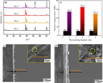
The X-ray diffraction patterns of the shot-peened and non-peened samples are displayed in Fig. 1a. As the figure shows, the half-widths of the diffraction peaks shot-peened samples were wider than that of the non-peened (compare No.1 and Nos.2–4). For (200) and (211), the diffraction peak broadening is particularly obvious. The grain size is inversely proportional to the half-width, indicating that the residual stress generated by shot-peening treatment can refine the grains [24,25].
10 20 30 40 50 60 70
10 20 30 40 50 60 70
10 20 30 40 50 60 70
10 20 30 40 50 60 70
No.2
No.4
Intensity /a.
u.
(211)
(a)
No.3
2 °
No.1 (a)
(200)
(a) (a)
3 4 5 6 7 8 9
0 20 40 60 80
No.1 No.1
No.4 No.3
No.2
Surfa
ce res
idual
st
res
s
/MP
a
Shot-peening diameter /mm No.1
(b)
Oxide film
10μm
250nm (c)
Columnar crystal
Oxide film
10μm
250nm (d)
Dislocation cell
Figure 1. Surface characteristics of shot peening specimens of different diameters: XRD pattern (a), residual stress (b), surface morphology and the cross-section of anodic oxide film of Nos.1 (c) and 3 (d).
[image:4.596.102.501.235.558.2]relaxation and its value was decreased. During the shot-peening process, the high-speed impact of the steel ball causes a strong plastic deformation on the surface of the samples, resulting in a significant increase in residual stress, as a result, the grain is refined and more vacancy defects are formed [26,27]. The SEM morphologies of the anodic oxide film are shown in Figs. 1c and d, with all the samples consisting of anatase TiO2 and exhibiting a white film. The thickness of the oxide film on the
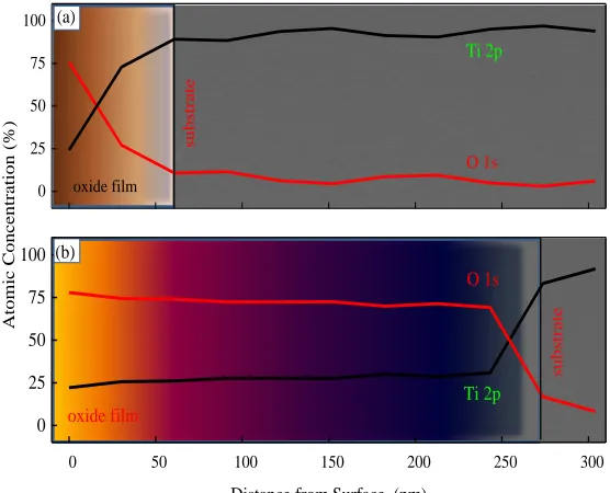
non-peened and shot-peened samples is measured to be ~60 and 270 nm, respectively (see Figs. 2(a) and (b)). Moreover, the oxidation film with higher residual stress has better crystallization performance. This mean that the thickness of the oxide film is controlled by residual stress. In addition, we can see that the shot-peened surface was characterized by the formation of small homogeneous nano-grains, which contain a large number of vacancies. However, the surface of the non-peened sample consists of micro-convex columnar crystals.
3.2 Defect thermodynamics and dynamics
In order to investigate the relationship between residual stress and surface free energy, the electromotive force was measured on the two electrodes. The shot-peened Ti13Nb13Zr electrode is used as the negative electrode of the battery, the Ti13Nb13Zr bulk electrode as the positive electrode. Based on this, the electrochemical reaction method is used to determine the thermodynamic function of shot-peened Ti13Nb13Zr, the electrode reaction equation is as follows:
Anode: (1) Cathode: (2) Cell reaction: (3) Based on the net reaction of the battery, combined with the relationship of the cell's electromotive force, temperature coefficient and reaction thermodynamic function, the following relational equation can be obtained:
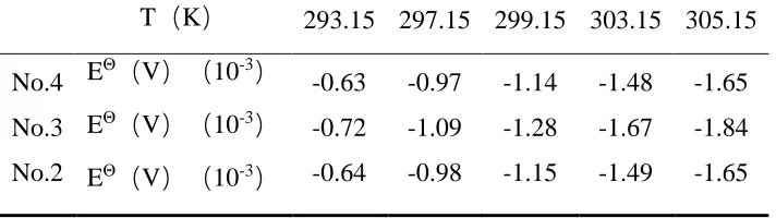
[image:5.596.122.478.631.731.2](4) Where z is the electronic measurement coefficient of the electrode reaction, F the Faraday constant, the standard electromotive force of the battery. Previous studies [28] have shown that , at T=298.15 K. The Gibbs free energy of on the shot-peened Ti13Nb13Zr surface at 298.15 K can be obtained from Eq. (4).
Table 2. Data on the change of cell electromotive force with temperature.
T(K) 293.15 297.15 299.15 303.15 305.15
No.4 No.3 No.2
EΘ(V)(10-3)
EΘ(V)(10-3)
EΘ(V)(10-3)
-0.63 -0.72 -0.64
-0.97 -1.09 -0.98
-1.14 -1.28 -1.15
-1.48 -1.67 -1.49
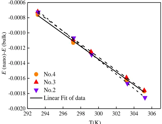
The electromotive force E of the primary battery composed of shot-peened Ti13Nb13Zr and bulk Ti13Nb13Zr electrodes was measured at different temperatures. The corresponding average electromotive forces are listed in Table 2 after five parallel experiments at each temperature. The electromotive force of the battery corresponds to the temperature, and the curve EΘ–T is shown in Fig. 2.
292 294 296 298 300 302 304 306
-0.0020 -0.0018 -0.0016 -0.0014 -0.0012 -0.0010 -0.0008 -0.0006
T(K)
E
(nan
o)-E
(bu
lk
)
No.4 No.3 No.2
[image:6.596.168.431.164.366.2]Linear Fit of data
Figure 2. Curves of electromotive force change with different temperatures.
A linear fitting equation was obtained with a linear fitting coefficient of 0.9993, the derivative of the fitting equation was further derived. Thus, the change coefficient of the electromotive force with temperature can be obtained. When T=298.15 K, the electromotive force of Nos.2, 3 and 4 are -1.05×10⁻³, -1.18×10⁻³ and -1.06×10⁻³ V respectively, the standard molar Gibbs free energy can be
obtained from Eq. (4), the nano-Ti13Nb13Zr samples of Nos.2, 3 and 4 under 298.15 K are 0.432, 0.44 and 0.41 kJ∙mol-1, respectively. The Gibbs free energy of shot-peened samples are higher 432, 440 and
410 times than that of the non-peened samples, respectively. Gibbs free energy is fitted to the residual stress, so that the curve can be obtained.
8.12 (5)
The Eq. (5) is further optimized to the exponential function:
(6) It can be seen from the Eq. (6) that the Gibbs free energy of the shot-peened sample can be improved. Simultaneously, the Gibbs free energy of increases first and then decreases, which is similar to the change law of surface residual compressive stress. The obtained fitting equation shows that the Gibbs free energy on the surface of Ti13Nb13Zr is exponentially related to the surface residual compressive stress.
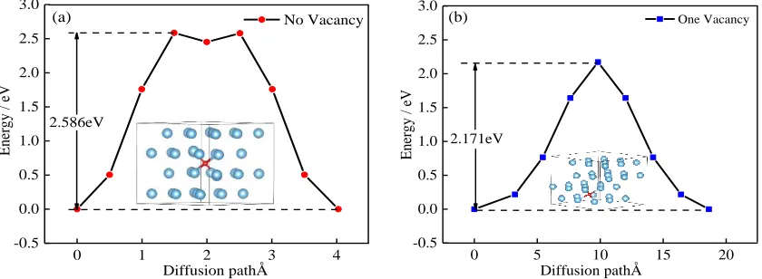
As shown in Fig. 3a, the diffusion path of crystal structures with no vacancies is an octahedron to a tetrahedron, then to an octahedron, then to an tetrahedron and finally to an octahedron. As shown in Fig.3b, the diffusion path of crystal structures with one vacancy is a tetrahedron to an octahedron and then to a tetrahedron. The atom's transition distance of the one vacancy structure was longer than that of the no vacancy structure (from 4.025 to 18.629 Å).Its value increased by 3.63 times and the diffusion barrier decreased by 16% (from 2.586 to 2.171 eV).
0 1 2 3 4
-0.5 0.0 0.5 1.0 1.5 2.0 2.5 3.0
En
ergy / e
V
Diffusion pathÅ
No Vacancy
2.586eV
(a)
0 5 10 15 20
-0.5 0.0 0.5 1.0 1.5 2.0 2.5 3.0
En
ergy / e
V
Diffusion pathÅ
One Vacancy
[image:7.596.90.510.197.351.2]2.171eV (b)
Figure 3. Diffusion barrier curves and diffusion path of O atoms in Ti.
According to the Winter-Zener theory [29], the corresponding diffusion constants, D0, were
3.37×10⁻⁷ and 2.89×10⁻⁷ m2/s. These values allowed the calculation of the diffusion coefficients of O atoms in the no and one vacancy Ti structures through an Arrhenius-type expression [30,31],
7 19 2 1
( ) 3.37 10 exp( 2.586 1.6 10 / )
D No vacancy− = − − − J KT m s− (7)
7 19 2 1
( ) 2.89 10 exp( 2.171 1.6 10 / )
D One vacancy− = − − − J KT m s−
The diffusion coefficients of the one vacancy structure were higher than that of the no vacancy structure (from 5.31×exp(-55) to 3.10×exp(-47)), its value increased by 1749 times. The greater ease with which O diffused in the one vacancy Ti confirmed the result concerning the diffusion barrier, which was found to be higher in the no vacancy structure.
3.3 Film structure characteristics
diffusion activation energy so that the diffusion of Ti and O ions is accelerated, the binding of Ti and O ion is promoted inside the matrix. This conclusion coincides with the vacancy model that is established in this study.
0 50 100 150 200 250 300
0 25 50 75 100
0 25 50 75 100 (b)
subst
rat
e
oxide film
Ti 2p
O 1s
sub
strate
oxide film
Ti 2p
O 1s
(a)
A
tomi
c Concentr
at
ion (%
)
[image:8.596.162.440.143.368.2]Distance from Surface (nm)
Figure 4. XPS depth sputtering profiles analysis.
The OM image and Raman spectrum of are depicted in Fig. 5. For the OM image of the non-peened sample (see Fig. 5a), in the black region, the vibration peaks in four spectra occur at Raman shifts of 144, 405, 530 and 650 cm-1. In the white region, there is only one vibration peak at 114 cm-1. This indicates that the white region contains only anatase TiO2 with short range order. However, for
the OM image of the shot-peened sample (see Fig. 5b), whether in the black or in the white region, these vibration peaks occur at Raman shifts of 144, 399, 516 and 639 cm–1.
0 200 400 600 800 1000
(a)
Raman shift(cm-1)
640
(cm
-1)
530
(cm
-1)
405
(cm
-1)
154
(cm
-1) (a)
0 200 400 600 800 1000
(b)
620
(cm
-1)
508
(cm
-1)
405(cm
-1)
154
(cm
-1)
Raman shift(cm-1)
[image:8.596.100.500.545.714.2]This means that anatase TiO2 with long range and short range order coexist in these two
regions. Moreover, the boundary of the shot-peened samples between the black and white regions became somewhat blurred, which indicated that the shot-peening treatment played a positive role in the crystallization process. Compared with reference [34], we obtain a similar conclusion that the crystallinity of the anodic oxide film on surface nano-crystallization is obviously higher than that of the non-peened sample.
3.4 Corrosion resistance
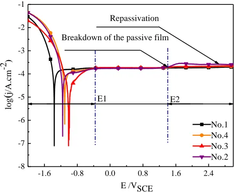
To investigate the corrosion behavior before and after shot-peening treatment, potentiodynamic polarization tests were carried out on Ti13Nb13Zr samples, in 0.9 wt.% NaCl solution (Fig. 6).The curve is divided into a cathode and an anode region. On the cathodic branch, the main reaction is the hydrogen evolution reaction. On the anodic branch, the oxygen precipitation reaction (i.e., titanium oxidation) occurs. A wide passive region from −1.15 to −0.30 VSCE with current density ~ −1 μA cm−2
was observed after a short active dissolution for the shot-peened samples. In contrast, a narrow passive region existed for the untreated samples from −1.35 to −1.20 VSCE. Corrosion resistance behavior is
exhibited in the region in which the samples are passive. The current increases for shot-peened samples at a potential up to −0.3 VSCE. In the E1 to E2 region, the current density remains unchanged.
This is because a low conductivity passivation film is formed on the surface of theTi13Nb13Zr during the anodization process. When the potential rises to E2=1.5 VSCE, the current density of No.4 suddenly
increases, and then the phenomenon of repassivation occurs, passivation film causes the electronic conductance to be delayed as it passes through the oxide film, eventually leading to a constant current. Oliveira et al. and Tavares et al. [35,36] indicate that the passive film is breaking. However, the current range is set rapidly as per the repassivation of the metal.
-1.6 -0.8 0.0 0.8 1.6 2.4
-8 -7 -6 -5 -4 -3 -2 -1
E2 Repassivation
Breakdown of the passive film
E /VSCE
log
(
j/A.cm
-2 )
[image:9.596.179.421.507.705.2]No.1 No.4 No.3 No.2 E1
For the non-peened sample, it translated directly into the passive region from the Tafel region from −1.20 to 3 VSCE, and exhibited a typical self-passivation characterization. However, the
non-peened sample (shot-diameter of 6 mm) experiences several active passive transitions from −1.15 to 0.14 VSCE and then tends to passivation again. This indicates the formation of a passive film that is not
sufficiently protective under immersion into the electrolyte, and in the active-passive region, the corrosion rate increased [37]. According to Geetha et al. [38], the phenomenon of metal repassivation also plays an important role in the alloy's corrosion behavior. Titanium alloys show a faster repassivation phenomenon than stainless steel. This provides excellent corrosion resistance for shot-peened samples [39–41].
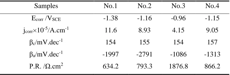
The corrosion potential (Ecorr), corrosion current density (icorr), anodic and cathodic Tafel slopes (βa and βc) of the materials were determined by Tafel analysis of these branches of the polarization curves using EC-Lab software (see Table 3). It can be seen that the Ecorr (i.e.,
self-corrosion potential) of the shot-peened sample was higher than that of the non-peened sample. The Ecorr increased by 30.4% (from -0.96 to-1.38 V), the jcorr (i.e., self-corrosion current density) of the
shot-peened sample was lower than that of the non-peened sample and the jcorr decreased by 2.8 times
[image:10.596.104.496.383.512.2](from 11.6×10-5 to 4.15×10-5 A.cm-2).
Table 3. Electrochemical parameters of samples in 0.9 wt.% NaCl solution.
Samples No.1 No.2 No.3 No.4
Ecorr /VSCE
jcorr×10-5/A.cm-1
βc/mV.dec-1
βa/mV.dec-1
P.R. /Ω.cm2
-1.38 11.6
154 -1997 634.2
-1.16 8.93
155 -2791 793.3
-0.96 4.15 154 -1086 1876.8
-1.15 9.05
157 -1313 866.2
Compared with the corrosion potential (Ecorr) of the untreated sample, this increase represents the achievement of a more noble electrode potential, and indicates an improved corrosion resistance of the Ti13Nb13Zr following shot-peened treatment. The corrosion current density is characterized as an important parameter for evaluating the corrosion reaction kinetics [42]. The metal corrosion rate is normally proportional to the corrosion current density, as measured by Tafel plots, and the lower current density implies a lower corrosion rate. In addition, the polarization resistance (P.R.) of the Tafel curves was calculated using the Stern–Geary equation.
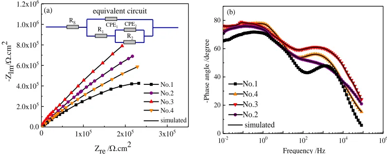
The shot-peened sample data and non-peened sample measured after 600 s of immersion in the 0.9 wt.% NaCl solution at 25 °C are presented in Fig. 7. The Nyquist plots for all samples exhibit an incomplete and capacitive-like semicircle (see Fig. 7a). This phenomenon is related to the charge transfer reaction from the sample surface to the electrolyte through the double electrochemical layer [43]. The semicircle diameter of the shot-peened samples is significantly larger than that of the non-peened sample. An increase in the semicircle indicates an increase in film stability and a decrease in semicircle diameter indicates a decrease in passive film resistance. A similar trend was observed in the impedance spectra of some Ti alloys [16,44]. The corresponding Bode magnitude plots have two characteristic regions and are presented in Fig. 7b. The high frequency region of the Bode phase diagram is characterized by a phase angle of ~0°, corresponding to the electrolyte resistance. Similarly, a phase angle of approximately −80° in the intermediate-frequency region is indicative of a capacitive load. A sharp peak phase angle occurs in each of the high- and low-frequency regions, consistently with the formation of a duplex passive film structure (a compact inner layer and a porous outer layer) on Ti [45].
No.1 No.2 No.3 No.4 simulated
0 1x10⁵ 2x10⁵ 3x10⁵
0.0 2.0x10⁵ 4.0x10⁵ 6.0x10⁵ 8.0x10⁵ 1.0x10⁶ 1.2x10⁶
R2
CPE1 CPE2
RS
-Z
lm
/
.cm
2
Zre /.cm2
R1
(a) equivalent circuit
10-2 100 102 104 106 0
20 40 60 80
Frequency /Hz
-Phase angle /degre
e
[image:11.596.99.497.332.490.2]No.1 No.4 No.3 No.2 simulated (b)
Figure 7. Nyquist plots (a) and Bode plots (b) of the samples in 3.5% wt. NaCl.
The equivalent circuit (see Fig.c7a) was selected based on the EIS results and the fitting of the experimental data with the ZSimpWin software. An Rs((CPE1 R1(CPE2 R2))) circuit model with two
time constants was used to fit the passive film obtained. In the equivalent circuit (Fig. 7a), RS
represents the solution resistance; CPE1 and CPE2 denote the constant phase elements
[46],corresponding to the non-ideal capacitances of the porous outer layer and the compact inner layer, respectively; R1 and R2 represent the resistance of the porous outer and compact inner layer,
respectively [47,48].
The electrochemical parameters obtained from the equivalent circuit are listed in Table 4. The low value (~10−3) of χ2 indicates that the test results correspond closely to the fitting results. As can be seen from Table 4, the R2 values of the shot-peened samples are significantly larger than that of the
non-peened sample. The R2 values are strongly dependent on the passive film characteristic and
corrosion resistance of the materials. A higher R2 value implies good corrosion resistance. A decrease
Table 4. EIS experimental data in 0.9wt.% NaCl solution.
Samples No.1 No.2 No.3 No.4
CPE1(μF.cm-2)
CPE2(μF.cm-2)
Rs(Ω.cm2)
R1(kΩ.cm2)
R2(kΩ.cm2)
χ2(10-4)
11.925 12.92 13.53 0.521 6.07E16
0.82
56.40 0.12 13.61 6.997 8.6E16
3.95
10.535 0.97 13.14 7.719 1.0E17
1.34
21.69 2.89 13.59 6.174 8.0E16
1.92
According to previous studies [20,50], the high reactivity of titanium with oxygen ensures the formation of the passive film that protects the surface of the treated sample, which is consistent with the conclusion of the diffusion of oxygen on the titanium surface.
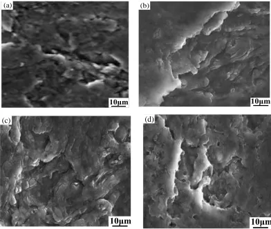
The surface morphologies of the non-peened and shot-peened samples after being immersed in 0.9 wt.% NaCl solution for 240 h are shown in Fig. 8. The cracks of the oxide film on the surface of the shot-peened sample were all smaller than that of the non-peened sample (see Figs.8a–d).
10μm (a)
10μm (b)
10μm
(c)
10μm
(d)
[image:12.596.100.492.388.719.2]In addition, after 10 days of immersion, there are only some corrosion holes with a small diameter on the surface of the shot-peened sample. The corrosion hole decreases first and then increases with the decrease of shot-peening diameter. When the diameter of shot peening is 6 mm, the corrosion pores disappear and the anodic oxide film is relatively smooth. According to electrochemical and immersion tests, the shot-peening process promotes the corrosion resistance behavior of Ti13Nb13Zr in the 0.9 wt.% NaCl solution. This is consistent with the corrosion potential, the corrosion current density, more noble passive region and R2 results reported previously. It is due to the
repeated impact provided by the balls on its surface, resulting in a large amount of surface free energy and vacancies in the surface during the shot-peening process [15].
3.5 Mott-Schottky and donor density analysis
The Mott-Schottky curve and the donor density of the oxide film for the non-peened and shot peened samples at the 3VSCE potential are presented in Fig.9, the Mott-Schottky curves of all the
samples showed a straight line with a positive slope, which indicates that the oxide film formed by the anodization is an n-type semiconductor, and the oxide film of the n-type semiconductor is dominated by vacancy defects. This indicates that the more oxygen vacancies, the better the thickness and crystallization performance of the oxide film [51,52].
-0.8 -0.4 0.0 0.4 0.8 1.2
0.0
2.0x10⁸
4.0x10⁸
6.0x10⁸
8.0x10⁸
1.0x10⁹
No.1 No.2 No.3 No.4
Potential / VSCE
C
-2 /F
-2
cm
4
(a)
3 4 5 6 7 8 9
0.0
2.0x10²³
4.0x10²³
6.0x10²³
8.0x10²³
1.0x1024
1.2x1024
No.1 No.1
No.4
No.3 No.2
Don
or
den
stry
/cm
3
Shot-peening diameter /mm No.1
[image:13.596.70.528.384.552.2](b)
Figure 9. Mott-Schottky analysis (a) and donor density of samples in 3.5% wt. NaCl (b).
The longest straight line of the Mott-Schottky curve is tangented, and the positive slope is calculated from the tangent, the donor concentration ND can be calculated from the positive slope.
(9) Where α is the tangent slope; e the electronic charge (1.60×10⁻¹⁹C), ε0 the vacuum dielectric
constant (8.85×10⁻¹⁴ F/cm), ε the relative permittivity (80 for TiO2), ND is the donor density. The
donor density of the oxide film is shown in Fig. 9b. The donor density of the shot-peened sample is lower than that of the non-peened sample, with the donor density decreasing five-fold (from 1.05×10⁻²⁴ to 5.25 × 10⁻²⁵ cm -3). Meanwhile, with the decrease of shot-peening diameter, the donor density increases first and
stable growth of the oxide film during the anodization process. The oxide film can prevent the charge transfer and further prevent the electrochemical reaction, so as to slow down the dissolution and corrosion of oxide film [53-55]. According to previous studies [56], the flat band potential (EFB) and the donor density (ND) of the anodic films formed on Ti electrode are dependent on the oxide film thickness. On increasing the film thickness the flat band potential is shifted to more negative values and the donor density decreases, enhancing the dielectric characteristics of the titanium oxide.
4. CONCLUSIONS
1) The residual stress of the Ti13Nb13Zr surface was significantly increased by shot-peening. When the diameter of shot-peening was 6mm, the residual stress of the shot-peened sample was higher than that of the non-peened sample, and its value increased by 5.9 times (from 10.17 to 65.3 MPa). With the decrease of the shot-peening diameter, the plastic deformation gradually intensifies. When the plastic deformation reaches the critical value, the surface of the material begins to crack, which makes the residual stress increase first and then decrease.
2) The residual stress generated by shot-peening effectively increases the surface Gibbs free energy of Ti13Nb13Zr. When the diameter of shot-peening is 6mm, the standard molar Gibbs free energy on the surface of the sample with shot-peened treatment was higher than that of the non-peened sample, and its value increased by 440 times (from 0.01 to 0.44 kJ∙mol-1). The functional relationship between the residual stress and Gibbs free energy was established by a polynomial fitting method:
.
3) The residual stress generated by shot-peening significantly increases the thickness and crystallinity of the anodized film on the surface of Ti13Nb13Zr. At the shot-peening diameter of 6mm, the thickness of the oxide film is as high as 273 nm, which is about 4.71 times that of the non-peened sample. Compared with the non-peened sample, the content of Ti2p on the surface with shot-peening treatment decreased from 73% to 18% and the O1s content increased from 23% to 78%.
4) The residual stress generated by shot-peening significantly improved the corrosion resistance of the Ti13Nb13Zr anodized surface. The self-corrosion potential increased from -1.38 to -0.96 V and the self-corrosion current density decreased from 1.16× 10 -4 to 4.15 × 10⁻⁵ A.cm-1. The maximum increase and decrease of the self-corrosion current density were 30.4% and 64.2%, respectively. At a shot-peening diameter of 6 mm, the carrier density of the shot-peened sample is lower than that of the non-peened sample. Its value decreased by 5 times (from 1.05×10⁻²⁴ to 5.25×10⁻²⁵ cm-3), with the
decrease of donor density, the channel of Cl- ion transport is effectively reduced.
ACKNOWLEDGEMENTS
References
1. A. Koyun, A. B. H. Yoruc, H. E.O. Elkoca, Ind. Lubr. Tribol., 66(2014) 106–110. 2. D. Xiong, Y. Yang, Y. Deng, Surf. Coat. Tech., 228 (2013) 442–445.
3. D. Quintero, O. Galvis, J. A. Calderón, J. G. Castaño, F. Echeverría, Surf. Coat. Tech., 258 (2014) 1223–1231.
4. R. D. Ramdan, J. R. P. Djuansjah, M. R. A. Kadir, H. Nur, E. Hamzah, Adv. Mater. Res., 650 (2013) 12–17.
5. L. Benea, E. Danaila, P. Ponthiaux, Corros. Sci., 91 (2015) 262–271.
6. R. Tsaryk, K. Peters, S. Barth, R. E. Unger, D. Scharnweber, C. J. Kirkpatrick, Biomaterials, 34 (2013) 8075–8085.
7. G. A. El-Mahdy,Corrosion. 63 (2007) 299–306.
8. M. Tian, W. G. Pell, B. E. Conway,J. Electroanal. Chem., 552 (2003) 279–290.
9. N. Wang, W. Zhang, J. Xu, B. Ma, Z. Zhang, Q. Jin, J. Solid State Electr., 14 (2010) 1377–1382. 10. X. Yu, Y. Li, W. Ge, Q. Yang, N. Zhu, K. Kalantarzadeh, Nanotechnology, 17 (2006) 808-810. 11. X. H. Yu, Z. L. Zhan, J. Rong, Z. Liu, L. LI, J. Liu, Chem. Phys. Lett., 600 (2014) 43–45. 12. X. H. Yu, R. Ju, Z. L. Zhan, Z. Liu, J. Liu, Mater. Design., 83 (2015) 159–163
13. O. Stein, J. Ankri, M. Asscher, Phys. Chem. Chem. Phys., 15 (2013) 13506 –13512.
14. T. Hu, K. Ma, T. D. Topping, J. M. Schoenung, E. J. Lavernia, Acta Mater., 61 (2013) 2163–2178. 15. Y. Zheng, H. L. Yang, Y. Wang, Z. Xu, X. H. Yu, T.Mater. Heat Treat., 37 (2016) 203–208. 16. T. Fu, Z.L. Zhan, L. Zhang, Y. Yang, Z. Liu, J. Liu, Surf. Coat. Tech., 280 (2015) 129–135. 17. H. F. Tang, Z. Y. Huang, M. Xiao, J. Nanopart. Res., 19 (2017) 312–318.
18. G. Kresse, J. Furthmüller, Phys. Rev. B, 54 (1996) 11169. 19. X. H. Yu, Z. L. Zhan,Nano. Res. Lett.,9 (2014) 516–521.
20. X. Wang, X. H. Yu, Z. L. Zhan,Mater. Res. Express, 5 (2018) 095010.
21. J. P. Perdew, K. Burke, M. Ernzerhof, Phys. Rev. Lett., 77 (1998) 3865–3868. 22. P. E. Blöchl, Phys. Rev. B, 50 (1994) 17953–17979.
23. G. Henkelman, B. P. Uberuaga, H. Jónsson, J. Chem. Phys., 113 (2000) 9901–9904.
24. J. Makni-Chakroun, W.Cheikhrouhou-Koubaa, M. Koubaa,A.Cheikhrouhou,J. Alloy Compd., 650 (2015) 421–429.
25. Y. F. Shen, J. Tang, Z. H. Nie, Y. D. Wang, Y. Ren,L. Zuo,Bio. Resource Technol., 100(2009) 4139–4145.
26. M. Sebastiani, M. Piccoli, E. Bemporad, Surf. Coat. Tech., 215 (2013) 407–412. 27. J. C. Kim, S. K. Cheong, H. Noguchi, Int. J. Fatigue, 55 (2013) 147–157. 28. J. Lindemann, Canf. Buque, F. Appel, Acta Mater., 54 (2006) 1155–1164. 29. C. Wert, C. Zener, Phys. Rev., 76 (1949) 1169–1175.
30. K. Villars, W. B. Cenzual, A. Pearson, Mater. Park, 60 (2011) 13–14. 31. K. J. Laidler, Chem. Educ., 61 (1984) 494–450.
32. T.Y. Sul, C.B. Johansson, S. Petronis, A. Krozer, Y. Jeong, A. Wennerberg, Biomaterials, 23 (2002) 491-501.
33. A. Karambakhsh, A. Afshar, S. Ghahramani, P. Malekinejad, J. Mater. Eng. Perform, 20 (2011) 1690-1696.
34. Zhi. W. Wang, R. J. Diao, Zhen. T. Yuan, Xiao. H. Yu, Tian. L. Fu, Y. Zhao, Zhao. L. Zhan, Int. J. Electrochem. Sci., 13 (2018) 4411-4423.
35. V.M.C.A. Oliveira, C. Aguiar, A.M. Vazquez, Robin. A, Barboza. M. J. R, Corros. Sci., 88 (2014) 317–327.
36. A.M.G. Tavares, B.S. Fernandes, S.A. Souza, J. Alloys Compd., 591 (2014) 91–99. 37. F. Xie, X. He, S. Cao, Electrochim. Acta, 105 (2013) 121–129.
40. T. Li, L. Liu, B. Zhang, Electrochem. Commun., 52 (2015) 80–84.
41. H. Jang, C. Park, H. Kwon H. Jang, C. Park, H. Kwon, Electrochim. Acta, 50 (16–17) (2005) 3503–3508.
42. P. Handzlik, K. Fitzner, Trans. Nonferrous Metals.Soc. China 23 (3) (2013) 866–875. 43. S. Ningshen, U. Kamachi Mudali, S. Ramya, Corros. Sci., 53 (1) (2011) 64–70.
44. J. Jayaraj, A. Ravi Shankar, U. Kamachi Mudali, Electrochim. Acta, 85 (2012) 210–219. 45. A. M. Fekry, R. M. EI-Sherif, Electrochim. Acta, 54(2009) 7280-7285.
46. F. Rosalbino, D. Macciò, G. Scavino, A. Saccone, J. Mater. Sci. - Mater. Med., 23(2012)865-871.
47. S.A. Fadl-Allah, Q. Mohsen, Appl. Surf. Sci., 256 (2010) 5849-5855.
48. Rui. J. Diao, J. Rong, X. Wang, Yu. H. Yao, Zhao. L. Zhan, Xiao. H. Yu, Int. J. Electrochem. Sci., 13 (2018)7765-7777.
49. N.T.C. Oliveira, A.C. Guastaldi. Acta. Biomater., 5 (2009) 399.
50. Macdonald. D. D, Biaggio. S. R, Song. H, J. Electrochem. Soc., 139 (1992) 170-176. 51. A. Cigada, M. Cabrini, P. Pedeferri, J. Mater. Sci. Mater. Med., 3 (1992) 408-412.
52. H. Habazaki, M. Uozumi, H. Konno, K. Shimizu, P. Skeldon, G.E. Thompson, Corros. Sci., 45 (2003) 2063-2073.
53. M. C. Chu, M. J. Singh, P. T. Liu, H. P. D. Shieh, H. C. You, Y. W. Tu, Applied Phys. Express, 6 (2013) 249–257.
54. J. I. Kim, K. H. Ji, M. Jang, H. Yang, R. Choi, J. K. Jeong, Acs. Appl. Mater. Interf., 3 (2011) 2522–2528.
55. X. Wang, J. Rong, Y. H. Yao, J. Feng, Y. N. Zhang, X. H. Yu, Z.L. Zhan, Int. J. Electrochem. Sci., 13 (2018) 9731–9741.
56. M.A. Schmidt, D. S. Azambuja, E. M. A. Martini, Corros. Sci., 48 (2006) 2901-2912.