RIT Scholar Works
Theses
Thesis/Dissertation Collections
1-2005
The development and performance evaluation of
PIF logic functional blocks
Sheetal Suresh Sonar-Pardeshi
Follow this and additional works at:
http://scholarworks.rit.edu/theses
This Thesis is brought to you for free and open access by the Thesis/Dissertation Collections at RIT Scholar Works. It has been accepted for inclusion
in Theses by an authorized administrator of RIT Scholar Works. For more information, please contact
Recommended Citation
Logic Functional Blocks
By
Sheetal Suresh Sonar-Pardeshi
In Partial fulfillment
of the
Requirements for the degree of
MASTER OF SCIENCE
In
Electrical Engineering
Approved by:
Professor
---
D. Patru
(Dr. DORIN PATRU, Thesis Advisor)
Professor
---
P. R.
Mukund
(Dr. P R MUKUND, Thesis Committee Member)
Professor
---
James
E.
Moon
(Dr. JAMES MOON, Thesis Committee Member)
Professor _____________
R_o_b
___
e_r_t _B_o_w
___ m
___ a_n
__________________ _
(Dr. ROBERT BOWMAN, Department Head)
DEPARTMENT OF ELECTRICAL ENGINEERING
KA TE GLEASON COLLEGE OF ENGINEERING
ROCHESTER INSTITUTE OF TECHNOLOGY
ROCHESTER, NEW YORK, USA
Title
ofThesis: The Development
andPerformance Evaluation
ofPD7 Logic
Functional
Blocks
Name
ofAuthor: Sheetal Suresh Sonar-Pardeshi
Degree: Master
ofScience
Major: Electrical
Engineering
College:
Kate Gleason College
ofEngineering
As
per currentRochester Institute
ofTechnology
(RIT)
guidelinesfor
completionof
my
degree,
I
understandthat
I
needto
submit acopy
ofmy Master's
thesis to the
RIT
Archives.
I
hereby
permitRIT
andits
agentsto
archive and make use ofmy
thesis
ordissertation in
whateverforms
necessary.I
retainthe
ownership
rightsto
the
copyright ofthe thesis
ordissertation
and also retainthe
rightsto
use all orpartofmy
thesis
in
my
future
work.Acknowledgements
I
wouldlike
to
thankthe
people who contributedtowards the
success ofthis
thesis.
I
willstartwiththe
Supreme
Being, GOD,
for his blessings.
I
amvery
muchgrateful andwill
be
soforever
to
my
parents, Dr.
Suresh
Sonar
andMrs. Nanda Sonar
and
my
family (Smita,
Ashwini
andSahil)
for
theirinspiration
and moralsupport;
I
owemy every
successto them.
I
have learned
alot from
Dr. Dorin
Patru,
my
thesis
advisor notjust
aboutdigital
design but
also about practical aspects oflife.
I
thank
Dr. Patru
for
many insightful
conversations
during
the
development
ofthe
ideas in
this
thesis,
andfor
helpful
comments on
the text.
Also for
the
freedom he has
allowed meto
makemy
owndecisions
during
the
design
anddevelopment
work.His
intelligence
andwisdomis
whathas
madethis thesis
possible.I
wouldlike
to thank
my
committeemembers, Dr. P R
Mukund
andDr.
James
Moon
for
taking
outtime
from
their
busy
scheduleto
reviewmy
work.Finally,
I
wouldlike
to
thankour systemadministratorMr. James
Stefano
for providing
allthe
necessary
Abstract
In
the
deep
submicron range ofIntegrated circuitdesign,
interconnects
and notthe
logical
gates arecausing
the
performancebottleneck.
The
number of availabletransistors
increase
by
afactor
of2 every
technology
nodebut interconnects do
not scalewithdevices,
devices
scaledown
faster
andthus the
presentdesigns
needto
be
scalable andreusable.
Pipeline
interconnect free
(PIF)
logic
methodology
has
a potentialto
solvethese
current
design
problems.In PEF
logic
design methodology
the
globalinterconnects
arereplaced
by
chain oflogical
gates.PIF
logic
usesonly
onetype
of gatewhichcanbe
connected
only
to the
adjacent eight gatesmaking
the
gate andthe
interconnect
modeling
easier.
In
orderto
migratefrom
onetechnology
nodeto other,
just
onePIF
cell needsto
be
redesigned.The PIF
cellin
newtechnology
node can replacethe
present cellsthus
making PIF
logic based
circuitsfully
reusable.This
thesis
implements
PIF
design methodology
to
develop
two
libraries
consisting
ofcombinational and sequentialfunctional
blocks
such asadder,
shiftregisters, multiplexers,
decoders
and encoders.The
performance ofthese
functional
blocks is
comparedwiththe
standard cellimplementation
withrespectto the
quality
Table
ofContents
Acknowledgements
iii
Abstract
iv
Table
ofContents
vTable
ofFigures
ix
Chapter 1: Introduction
1
1
.1
Scope
ofResearch
2
1
.2Organization
ofThesis
2
Chapter 2: Background
work4
2.1
Global Interconnect
4
2
.2 Power Management
5
2
.3
Scaling
andreusability
6
2.4 Device
andProcess modeling
6
2.5 Non-CMOS
device
7
2.6
Yield Enhancement
7
Chapter 3: PD7
logic design methodology
andfew
examples9
3. 1 PIF
logic
definition
9
3.2 Introduction
ofPIF cells10
3.3
PU
logic design
rules13
3.5 PIF
logic
performanceanalysis18
3.6
Conclusion
20
Chapter
4: Multiplexer based PIF logic design
21
4.1 PIFNAND
design limitations
21
4.2 Need
for
a newPIF
cell22
4.3
Why
transmission
gatetopology
23
4.4 PIF
multiplexertopology
25
4.5 Layout
of4-to-l
multiplexer28
4.6
Examples
ofPIF
logic implementation
30
4.6. 1 Multiplexer
30
4.7 Performance
assessment 344.7.1 Power
dissipation
calculation35
4.7.2 Propagation
delay
measurement36
4.8
Simulation
results of2-to-l
multiplexer38
4.9
Comparison
ofQuality
metricsfor
of2-to-l
multiplexer40
4.10 Multiplexer 4-to-l
45
4.11 Functional Verification
andSimulation
Results
of4-to-l
Multiplexer
48
4.12 Multiplexer 8-to-l
52
4.13 Functional Verification
andSimulation Results
of8-to-l
Multiplexer
56
4.14.
One bit full
adderdesign
61
4.15 Functional Verification
andSimulation
Results
of1
Bit
full
adder65
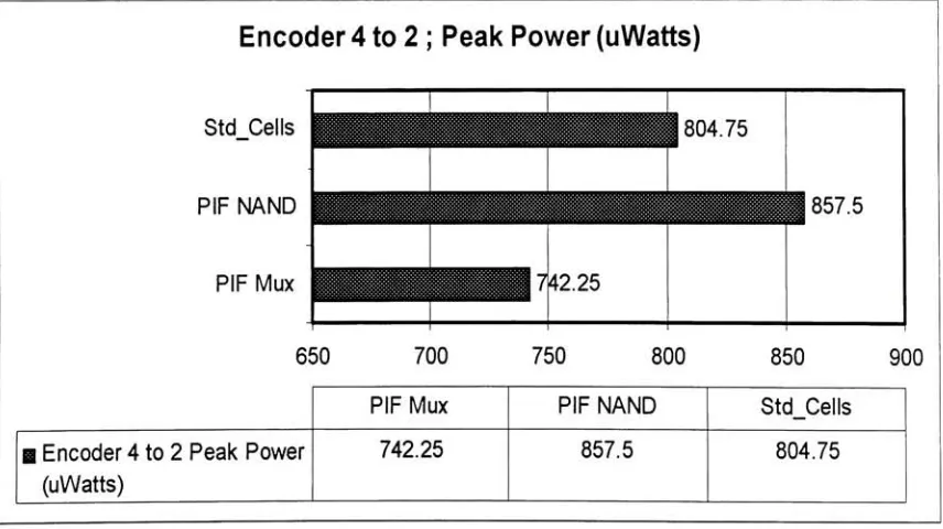
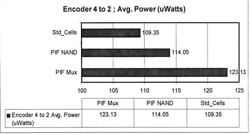
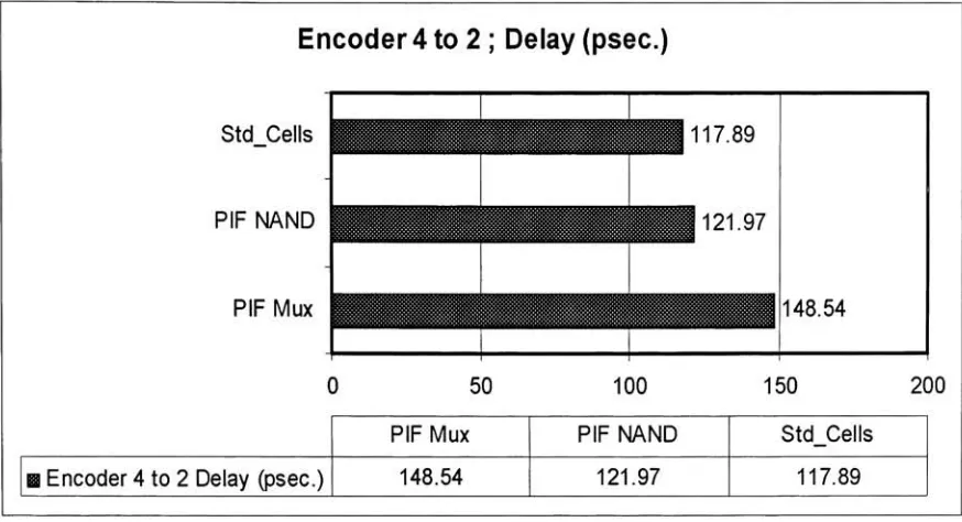
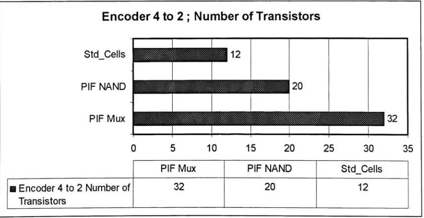
Chapter 5: Encoders
71
5.1
Standard
cell4-to-2
encoder71
5.2 PIF
logic
4-to-2
encoder73
5.3 Functional Verification
andSimulation Results
of4-to-2
encoder75
5.4 Encoder 8-to-3
80
5.5 Functional
Verification
andSimulation Results
of8-to-3
encoder84
5.6
Conclusion
89
Chapter 6: Decoders
90
6. 1
Standard
cells2-to-4 decoder
90
6.2 PIF
logic
2-to-4
decoder
92
6.3 Functional Verification
andSimulation Results
of2-to-4 decoder
95
6.4 Decoder 3-to-8
100
6.5 Functional Verification
andSimulation Results
of2-to-4
decoder
106
6.6 Conclusion
111
Chapter 7:
Shift
registers112
7.1 Master-slave D
flip
flop
112
7.1.1 D
flip
flop
withpreset and clear114
7.2 1
bit
shift register115
7.3 Functional Verification
andSimulation Results
of1
Bit Shift
register119
7.5 Functional Verification
andSimulation Results
of2 Bit
shift register128
7.6 4
bit
shift register134
7.7 Functional Verification
andSimulation
Results
of8 Bit
shiftregister138
7.8
Conclusion
143
Chapter 8:
Feasibility
ofPIF
logic
circuitsin
current andfuture
technologies
144
8.1 Throughput
in
PIF
logic based
circuits144
8.2 Power dissipation
in Current
andfuture
technologies146
Power dissipation
in
currenttechnologies
due
to
interconnects
146
Power dissipation in
future
technologiesdue
to
interconnects
148
Power dissipation in
future
technologies
due
to
leakage
currents150
8.3 Propagation
delay
predictionin future
technologies
152
8.4
Conclusion
1
52
Chapter 9: Conclusion
andfuture
work154
9. 1
Summary
1
54
9.2
Future
work155
References
157
Appendix
A;
Short forms
usedin
the
writeup
160
Appendix
B;
Simulation
Results
161
Table
ofFigures
Figure (3.2.1):
PIF
multiplexer astwo
input
AND
gate10
Figure (3.2.2):
PIF
multiplexer astwo
input
OR
gate1 1
Figure (3.2.3):
PIF
multiplexer astwo
input
NOR
gate11
Figure (3.2.4): PIF
multiplexer astwo
input
XORgate
12
Figure (3.2.5): PEF
multiplexer astwo
input
XNOR
gate12
Figure (3.4.1): NOT
gate,
PIF NAND
implementation
14
Figure
(3.4.2):
NOT gate, PIF
multiplexerimplementation
15
Figure
(3.4.3):
NOT
gate,
PIF
multiplexerimplementation
15
Figure (3.4.4): AND
gate,
PIF NAND implementation
16
Figure (3.4.5): OR
gate,
PIF
NAND implementation
16
Figure (3.4.6): NOR gate, PIF NAND
implementation
17
Figure (3.4.7):
XORgate,
PIF NAND
implementation
17
Figure (3.4.8): XNOR gate, PIF NAND implementation
18
Figure
4.3. 1
:Transmission
Gate
24
Figure (4.4.1): Transmission
gatebased
2-to-l
multiplexer26
Figure (4.4.2): Transmission
gatebased
4:1
Multiplexer
27
Figure (4.5.1): Stick diagram
for
PIF 4-to-l
multiplexer28
Figure (4.5.2): PIF
multiplexerlayout
in 0.25
utechnology
29
Figure (4.6.1): Standard
cellbased
2-to-l
Multiplexer
31
Figure (4.6.2): PIF NAND
based
2-to-l
Multiplexer
32
Figure
Figure
Figure
Figure
Figure
Figure
Figure
Figure
Figure
Figure
Figure
Figure
Figure
Figure
Figure
Figure
Figure
Figure
Figure
Figure
Figure
Figure
4.10.2):
PIF NAND
based
4-to-l Multiplexer
46
4.10.3): PIF
multiplexerbased
4-to-l
multiplexer47
4.12.1):
Standard
cellbased
8-to-l Multiplexer
53
4.12.2): PIF NAND
based
8-to-l
multiplexer54
4.12.3):
PIF
multiplexerbased
8-to-l
multiplexer55
4.14.1):
One bit full
adder,
standard cellimplementation
62
4.14.2.1):
One bit full
adder,
PIF NAND
implementation
63
4.14.2.2): One
bit full
adder, PIF
multiplexerimplementation
64
5.1.1): Encoder
4-to-2,
standard cellimplementation
72
5.2.1): Encoder
4-to-2,
PIF NAND
implementation
73
5.2.2): Encoder
4-to-2,
PIF Multiplexer
implementation
74
5.4.1): Encoder 8-to-3
standard cellsimplementation
81
5.4.2): PIF NAND
based
Encoder 8-to-3
82
5.4.3): PIF
multiplexerbased
Encoder 8-to-3
83
6.1.1):
Standard Cells
Decoder 2-to-4
92
6.2.1): Decoder
2-to-4;
PIF NAND
93
6.2.2): Decoder
2to4;
PIF Multiplexer
94
6.4.1): Decoder
3-to-8,
standard cellimplementation
102
6.4.2): Decoder
3-to-8,
PIF NAND
implementation
104
6.4.3): Decoder
3-to-8,
PIF
Multiplexer
implementation
105
7.1.1): D Latch
112
Figure
(7.1.3): Master-Slave
D
flip flop
withPreset
andClear
signals115
Figure (7.2.1):
IBit
shift registerStandard
cell116
Figure (7.2.2):
PIF
multiplexer1
Bit
shiftregister;
logical
depth
12
117
Figure (7.2.3):
PIF NAND 1 Bit
shiftregister;
maximumlogic
depth 17
118
Figure (7.4.1):
2Bit
shift registerStandard
cell125
Figure
(7.4.2):
2 Bit
shiftregister, PIF NAND
implementation
126
Figure
(7.3.3):
2Bit
Shift
register, PIF
multiplexerimplementation
127
Figure
(7.6.1):
Shift
register4
bit,
Standard
cellimplementation
134
Figure (7.6.2):
4 Bit
Shift
Register PIF NAND
136
The
integration
density
and performance ofintegrated
circuitshave
gonethrougha revolution.
The
device
sizeis shrinking
andas aresult, the
numberoftransistorsintegrated
on a singledie is increasing.
This
makesthe
modeling
ofdevices
andinterconnects
adifficult
task.
The
designs
produced sufferfrom
poorperformancedue
to
inaccurate
assumptions andinvalid
design
decisions
madeduring
design
simulation.The
mainsources of
the
variousproblems aredue
to
or relatedto
globalinterconnects,
andpower management.
Furthermore
due
to the
reductionin device
size, the
designs
needto
be
scalable and reusableto
be
usedin
the
newtechnology
node.A
lot
of researchhas been done
andis
stillgoing
onto
find
solutionsto these
problems,
such as multithreshold
devices,
organicdevices,
3
dimensional
interconnects,
interconnect
optimization,
delay
uncertainty
analysis,
selectivepowering
schemes.However,
thesesolutionstend to
workfor
a special problemunderspecial circumstances(as
canbe
understoodby
the
names).The
pipelinedinterconnect free
(PIF)
logic design
methodology
attemptsto
provide anapproach which addresses global
interconnects,
powerdissipation,
scalability
and
reusability
problems.In PIF
logic,
the
circuitinterconnects
are replacedwitha chainof gates.
The
resultant circuitdoes
nothave
any
globalinterconnects
except powersupply
lines
(VDD
andGND). The only
connectionspresentin
the
circuit arethe
local
interconnects between
the
neighboring
gates.A
schematicdesigned using PIF
logic
is
morestructured,
in
terms
of schematicdesign making it
device independent
andin
future
couldbe
usedfor
non-CMOSdevices.
1.1:
Scope
ofResearch
The
goalofthis
researchis
to
comparethe
performanceofPIF
logic
design
methodology
withstandard cellimplementation.
Various functional
blocks
areimplemented
in
both
the
design
methodologies and are comparedwithrespectto the
performance
quality
metrics such as powerdissipation,
propagationdelay
andlayout
area.
Three
different libraries
arebuilt,
2
based
onPIF
logic
and1
on standard cell.The
functional
blocks designed
aremultiplexers,
onebit
full
adder, encoders,
decoders
andshift registers.
The PIF
library
consists of1 1 schematics, 1 1
power schematics(the
circuits modified
to
obtain power consumptionresults)
and1 1
layouts
ofthe
abovementioned
blocks.
The
standard cellbased
library
consists of1 1
schematics andthe
layout
areais
calculatedfrom
the
availablelibrary.
Altogether 88
functional
blocks
aredesigned
(schematic
andlayout)
for
this
research.The
designs
areimplemented
in
0.25um
technology
using Cadence IC design
tools.
1.2: Organization
ofThesis
Chapter 2 describes
the
currentdesign
challenges andthe
solutions proposedby
others as
the
background
work.Chapter 3
presentsPIF
logic
design
rules and explainshow it
can provide a solutionto
some ofthe
currentdesign
problemsdiscussed in
PIF
andstandardcelllogic implementation.
Chapter
5
and6
explainthe
design
and comparison ofEncoders
andDecoders
respectively.
Chapter
7
deals
withthe
sequentiallogic
implementation
ofPIF
design,
the
shift registers and
their
comparison.Chapter
8
concludeswith asummary
andThe
design
challenges such as globalinterconnects,
powermanagement,
scaling
and
reusability,
device
and processmodeling
arediscussed
in detail
in
this
chapteralong
withsome of
the
solutions proposedby
other researchers.The
nextchapter willexplainthe
potential ofPIF
logic
methodology
to
provide a solutionto these
currentdesign
problems.
2.1: Global
Interconnect
For
efficient and predicTableimplementation
of alogic
circuit,
interconnect
planning
is
one ofthe
major challenges pointed outby
International
Technology
Roadmap
for
Semiconductors
(ITRS)
2004
edition.With
the
increase in
the
number oftransistors
perdie,
the
interconnect length is
alsoincreasing.
Interconnect
delays have
become
greaterthangatedelays
causing
synchronization problems[12]. With
increase in
wire
length
anddecrease in
wirewidth, the
interconnect
resistanceis
increasing
andmaking
it
to
behave like
atransmissionline causing
delay
anddata
errorsin
the
circuit[6]. As
aconsequence,
interconnect
analysisbecomes
more complex and correctinterconnect
modeling
is
becoming
more and moredifficult.
Significant
workhas been done
and continuesto
be
performedto
overcomethe
interconnect
andit's
modeling
problem.Three
dimensional
interconnects
areusedto
decrease
the
length
ofthe
globalinterconnect
andthus
reducing its
parasitic resistanceand capacitance
[7].
Interconnect
centricdesign
approachis
usedfor
gigascalesystem-on-a-chip
to
obtainanintegrated
architecturefor
globalinterconnects
[8].
Interconnects
circuit
design
performance[9].
2.2: Power
Management
Power
management andthe
leakage
current arethe
secondmajor challenge statedby
ITRS. The
power consumption of a circuitis divided into
two
categories: whenthe
devices in
the
circuit areswitching,
calleddynamic
power,
andwhenthe
devices
are notswitching,
called static power.During
transition
orswitching,
the
devices
performusefulworkof
changing
ormaintaining
the
logical
valuesin
the
circuit.Static
powerconsumption
is
causeddue
to
leakage
currentwhichflows
whenthe
transistoris
notswitching
oris
OFF
during
whichnouseful workis done.
In
sequentialcircuits, only
somedevices
areswitching
or some part offunctional
block
is
performing
useful work andthe
other partis
not;
that
is,
it is
wasting
the
powerin
the
form
of staticpowerdissipation.
Wise
use of powerwouldbe
reducing
staticconsumption
by
minimizing
the
idle
statetime
andobtaining
maximumthroughput
during
the
dynamic
orswitching
operation ofthe
circuit.The
management of poweris
applied atthe
systemlevel
using
static anddynamic
power reductiontechniques.
Static
technique
includes
synthesis and compilationdone for
low
powerdesign.
In
dynamic
technique,
runtime
behavior is
usedto
managethe
supply
voltage
to
different
parts ofthe
circuit;
this
is
calleddynamic
powermanagement(DPM).
One
ofthe
waysto
implement
DPM
is
by
dynamic
voltagescaling
whichis shutting
down
the
unusedI/O
devices [11].
Many
computing
devices
offer multiplesupply
the
power consumption ofthe
systemis
reducedandthenthe
powersupply
to the
devices
can
be
switchedback
againto
high
power statewhenthey
areperforming
usefulcomputation
[10].
2.3:
Scaling
andreusability
At every
technology
node, the
numberofavailabletransistorsincreases
by
afactor
of2. With
introduction
of new materialsfor
the
dielectric
and metallayers,
the
previously
designed
circuits are nolonger
useful and needto
be
redesigned.Interconnects
do
not scalewithdevices,
device
size changes more rapidly.Thus,
there
is
a needfor
the
designs
to
be
reusable and scalablewiththe
technology
in
orderto
copewiththe
changing
device
sizes.For
efficient andlow
costdesigns,
scaling
andreusability
is
necessary
andthus
is included
as one ofthe
major challengesin
the
ITRS
road map.Therefore,
designers
needto
comeup
withamethodology
that
willallowdesigns
to
be
scalable andfully
reusablefor
the
present andfuture
technology
nodes.This
willreduce
the time
requiredto
develop
the
previousdesigns
and alsothe
costinvolved.
2.4: Device
and processModeling
Introduction
ofnew materials and reductionin
device
sizetriggers the
rapid needofnew
device
models.The
simulationtools
also needto
be
updated withthe
latest device
models, to
obtain accurate and reliabledesigns.
The
fabrication
processesinvolved
alsoprocess
modeling
and makeremodeling
easieris
obviously
desirable.
2.5: Non-CMOS devices
Every
physicalquantity
has its
ownlimitations
andthe
conventionalCMOS
devices
are no exception.Thus,
peoplehave
startedto
look
at otherdevices like
crossbarlatches
of metal(introduced
by
Hewlett Packard
researchgroup
[15]),
organictransistors
[17]
and quantumlogic
[18]. The
crossbarlatch
is
abisTable
switch witha2
nanometerdevice
size.Organic
transistors
offer a wide range ofdevice
structures[16],
whilequantum
logic
makes use of single electron as atransistor.
These
devices
arein
the
primitive stage and need
to
be
modeled and characterizedin
orderto
be
usedin designs.
Introduction
ofthese
devices
also manifeststhe
needfor
reusabledesigns.
2.6:
Yield
enhancementThe
cost of anintegrated
circuitis
calculated as[4]:
Cost
perIC
=Variable
cost perIC
+(Fixed
cost/
volume)
where,
fixed
costis
the
effortin
time
and manpower neededto
producethe
design,
Volume
is
the
numberICs
produced andsold,
andVariable
cost=(cost
ofdie
+cost ofdie
test
+ cost ofpacking) / final
test
yieldwhere cost of
die is
givenas,
Cost
ofdie
=(cost
of
wafer)
/ dies
per wafer*die
yieldThe
cost of anIC
depends
on variablecostbecause
the
fixed
costis
constant asless
expensiveby increasing
the
volume of production whichrequireshigh
die
yield.Thus,
there
has
alwaysbeen
akeen
interest
and an attemptto
increase
the
yield.But
the
complexity
and stepsinvolved in
fabricating
adesign
on siliconwaferusing
opticalmasks
is increasing.
A
newdesign methodology
which usesless
number of metallayers
andthus
reduces
the
number ofstepsinvolved in fabrication is
needed.Each layer in
the
design
requiresseveral
processing
steps which costs money.If
the
number of steps requiredin
the
fabrication
processis
reduced, the
process variations andthe
errorcausing
sourceswill also
be
reduced,
thus
providing
high die
yield.For
time
and cost effectiveproducts,
This
chapterdeals
withthe
definition
ofPIF
logic
andintroduces
the
PIF
logic
design
rules.It
also explainsthe
potential ofthePIF
logic design
methodology
in
providing
a solutionto
some ofthe
currentdesign
problems.A
few
simplegateslike
NOT,
AND,
OR
and multiplexer are realizedin
PIF
logic
methodology.PIF
wasinitially
formulated
by
Richard Retanubun
[1]
in
2003. In
[20]
Vaibhav
has
extendedthe
work withaPIF
CAD
toolimplementation.
Interested
users can alsorefer
to their
workto
further
explorethe
PIF
logic design
methodology.3.1 PD7 logic definition
In
the
PIF
logic
only
onetype
of gateis
usedto
implement
the
entiredesign.
We
willcall
this the
gate orthe
PIF
cell.A
gatewhichcanimplement
any
arbitrary function
can
be
aPIF
cell.Examples
include
universalgatesNAND
orNOR,
which are completefunctions
in Boolean
algebra-i.e,
they
canimplement
any
otherfunction
and canbe
usedas
PIF
cell.For
this
research workwehave
usedtwo
different
gates1
.4-to-l
Multiplexer,
designed
as part ofthisresearch,
addressed asPIF
multiplexer
2.
Two
input
NAND
gate(NAND2),
Developed
by
Retanubun
[1]
asthe
first
PIF
gateimplementation,
addressed asPIF NAND
The NAND
gateis
the
gate of choiceinstead
ofthe
NOR
gatebecause
of smallinternal
parasitic(diffusion)
capacitances.The
reasonfor
selection of4-to-l
multiplexer3.2
Introduction
ofPIF
cell;
4-to-l Multiplexer
This
sectionintroduces
the
PIF
celldesigned
anddeveloped for
this thesis
andhow it
canbe
usedto
implement
any
two
variablefunction.
Minimum
two
input
gates arerequired
for
practicalpurposes, thus the
selection of4-to-l
multiplexeras aPIF
cell.Multiplexer
gateThe
output of a multiplexerdepends
onthe
logic
values ofits
selectline inputs.
PIF
logic design
methodology
makes use ofthe
selectlines
to
providethe
input
signalsand
the
data inputs
arehardwired
to
eitherVDD
orGND
depending
onthe
logic
function
implemented.
For
example,
AND
gateimplementation
using
multiplexeris
shownin
Figure
(3.2.1).
Figure
(3.2.
1): PIF
multiplexer astwo
input
AND
gateThe
output ofAND
gateis
logic
'1
'
only
whenboth
the
input
signals 'A' and 'B' areone,
elseit is
logic '0'. To
obtainthis
functionality,
inputs
'DO'hardwired
to
GND
and'D3'to
VDD.
Similarly,
two
input
OR, NOR, XOR,
XNOR
gates canbe implemented
using 4-to-l
multiplexer.
The
input
signalsare connectedto the
multiplexeras selectlines
andthe
data
inputs
'DO'through
'D3' areconnectedto
eitherVDD
orGND exactly in
the
samemanner as
the
outputlogic
that
appearsin
the
respectivetruthTables.
VDD
jWwiwWw
WiWWftWlMMiV
3$-3L
Q
Figure
(3.2.2):
PIF
multiplexerastwo
input
OR
gateHUX4 1
1;(*M**<W*(*M*M*W*
VDD
+f******r**r*rrrre *****&*>
MWW*w**ifif*i^?
?
WWWWKWW^+++++++f+r**+++*rr*++tirl.
Jrik.
0*
3
K(IHIilli>liWMMMttlIW
Figure
(3.2.4):
PIF
multiplexer astwo
input
XOR
gateGND
VDD
B
JTm
r*W*w***<*A*ft*ftafr'<**
Figure (3.2.5): PIF
multiplexer astwo
input
XNOR
gateThus,
multiplexer canimplement any
two
input
variable gatefunctionality.
These
gates can
be further
usedto
implement
the
arbitrary
functions
as canbe
seenin
the
3.3 PIF
Logic design
rules1.
Make
use ofonly
onetype
of gate.This
gate canbe
any
logic function
that
canbe
used
to
implement
any arbitrary
logic
function.
2.
On
atwo
dimensional
plane,
one gate canonly
be
connectedto the
eight adjacentgates.
3.
Output
of each gatedrives
one ortwo
inputs
ofthe
adjacentgates.But
for
better
delay balancing
in
this
pipelinedlogic, driving
two
inputs
is
preferred.For
example,
if
the
outputis
driving
a gatewhichis
in inverter
configuration,
thenit
should
drive
both
the
inputs
ofPIF NAND
gateimplementation
andboth
selectlines in
case ofPIF
multiplexerfor load balancing.
4.
If
output of a gateis
driving
two
different
gates,
thenonly
oneinput
of eachgateshould
be
connectedto the
outputpin ofdriving
gate andthe
unused pins onthe
loading
gates shouldbe
connectedto
VDD
in
caseofPIF NAND
gate andGND
in
case ofPIF
multiplexer.5.
Only
one gatedelay
is
allowedbetween
a signal andits inverted
value.In
case ofPIF NAND implementation
youhave
to
live
withthis
difference,
but in
case ofPIF
multiplexeroneadditional gatedelay
canbe
addedin
the
signalpath withoutinverting
the
logic
to
obtainthe
same gatedelay
between
a signal andits
complement.
A
circuitdesigned
using PIF
logic
rulesis
more structured.The
PIF
logic
methodology
circuit structure gives afloor
plan ofthelayout
asearly
asthe
gatelevel
design.
This
feature
ofPIF
logic
design
methodology
provesto
be
an advantagein
case3.4 PIF logic
implementation
ofBasic
gates1.
Inverter:
Both
the
inputs
ofNAND
gate are giventhe
same signalto
get aninverted
output
(Figure (3.4.1)).
?
WtWMWWWWWW
-v
MOOOOOOOOOMMMMHWMMMMMK
<-<<>:>*< <y>:**
Figure
(3.4.1):
NOT gate, PIF NAND
implementation
For
the
Multiplexer,
Inverter
canbe
implemented
in
two
waysi.
Input
signalis
givento
both
the
selectlines
anddata inputs
DO
andDl
areconnected
to
VDD
andD2
andD3
are connectedto
GND
to
getlogic
inversion,
seeFigure
(3.4.2).
ii.
Input
signalis
givenonly
to the
LSB
selectsignal(SO),
Figure
(3.4.3)
andDO
is
connectedto
VDD
andDl
to
GND,
restofthe
input
pinsareconnected
to
GND.
In
this
configuration,
one2-to-l
multiplexer and1
transmission
gatewithinthe
PIF
gate arethe
2
circuitswhichareswitching.
If only MSB
select signal(SI)
is
used asinput,
then
only
one2-to-1
multiplexer needsto
be
switched, saving
some peak powerFigure (3.4.2):
NOT gate, PIF
multiplexerimplementation
Figure (3.4.3):
NOT gate, PIF
multiplexerimplementation
3.
AND:
Input
signals are givento
oneNAND
gate andthen
it is followed
by
aninverter
as configuredin Figure (3.4.4).
In Multiplexer
implementation,
input
signals areconnected
to
selectlines
andthe
data inputs
are connected as seenA
B
mta
L>
mm'
AND
Figure
(3.4.4):
AND gate, PIF NAND
implementation
4.
OR
andNOR:
If
inverted
signals are givento
NAND gate,
it
acts asOR
gateproviding
a prooffor
De Morgan's
theorem
A=A+B
The
schematicfor
NAND
is
shownin
Figure
(3.4.5)
andfor
multiplexerin
Figure
(3.2.2).
For NOR
implementation,
aninverter is
connected atthe
output asshown
in
Figure
(3.4.6)
for
NAND.
'-nXH&H' :
;o
*ii*W
Figure
(3.4.5):
OR gate, PIF NAND
implementation
5.
XOR
andXNOR:
These
gates areimplemented
using
the
NOT
andOR
gatesas
discussed
above.The
resultantcircuits are shownin
Figures
(3.4.7)
for
C C C 60B 0 B ? > .^^ftiiiiiiim
rv~
Figure
(3.4.6):
NOR gate, PIF NAND
implementation
mm"^":^
mm'"
mmj'"""i
T )tMNH
Figure
(3.4.8):
XNOR gate, PIF NAND
implementation
3.5 PD7 logic
performance analysis3.5.1
Global Interconnect
The
PIF
logic
design
rule allows connectiononly
to the
neighboring
gateswhichmeans
that the
globalinterconnects
are nolonger
required(except
VDD
andGND)
andonly
local interconnects
are present.Most
ofthe
design
issues discussed
in Chapter
two
were
due
to
long
interconnects
andtheireffects on circuit performancelike increase
in
propagation
delay.
In
case ofthe two
adjacent cells connectedin
PIF
logic design
methodology,
nolarge
currentsflow
between
them,
so a minimumwidthwire canbe
used.
For
powersupply
lines
VDD
andGND,
the
placement of cellsis
suchthat the
VDD
and
GND
of each cell overlapswithVDD
andGND
of other cell respectively.The
powersupply
lines
are placedusing
the
top
metallayer,
thus
notdisturbing
the
metals usedfor
eliminating
the
long
interconnect
andbalancing
the
delay
throughthe
pipelining
ofPIF
cells.
3.5.2 Power
managementBy
using
the
sametype
ofcell,
the
powerdensity
is
uniformly
distributed
overthe
PIF
block.
Due
to the
organization ofthe
PIF
logic
andthe
intrinsic
pipelining,
the
gatesare utilized more
intensely,
reducing
the time
in
whichthere
is
no orvery
little
switching
activity.
More switching
of a gate means moredynamic
powerconsumed,
but
that
poweris
being
utilizedfor
computation.3.5.3
Scaling
andreusability
Due
to
the technological
changes,
a circuit needsto
be
redesignedmaking
the
previous
designs less
useful.This
makesscaling
andreusability
desired
propertiesofanew
design.
PIF
logic
circuitshave
these
propertiesinherently
because
the
design
uses asingle
PIF
cell.For
adesign
to
migratefrom
onetechnology
to
anotheronly
one cellhas
to
be
redesigned andthe
cellsin
the
previous circuit canbe
replacedby
the
new one.This
savesdevelopment
effortandimplicitly
time to
market.3.5.4
Non-CMOS devices
The PIF
logic design
methodology
is based
on afunctional
gate andis device
independent;
it
canbe
easily
implemented in
non-CMOSdevices.
Same design
rules needrules.
But
againonly
one cell needsto
be designed
and usedto
replacethe
CMOS
based
functional
gates.3.5.5 Yield
enhancementThe PIF
logic helps
to
enhancethe
die
yieldby
reducing
the
number of possiblefault
sources.Only
two
metals are neededfor local interconnections.
Reducing
the
number of metal
layers
also reducesthe
stepsinvolved in
the
manufacturing
process.Decreasing
the
number of steps also reducesthe
manufacturing
cost.3.6
Conclusion
This
chapterintroduced
PIF
design
rules and gave some examples ofhow
simple gatescan
be implemented in
PIF
logic design
methodology.The
currentdesign
challengesidentified
by
ITRS,
mentionedin
Chapter 2
werediscussed in
terms
ofPIF
logic design
methodology.
The
following
chapters providethe
variouscircuitsdesigned for
the
PIF
libraries
Chapter
4: Multiplexer Based PD7 Logic Design
In
the
previouschapter,
two
PIF
cells wereintroduced.
Both
ofthem
have
their
advantages and
disadvantages.
In
this
chapter wewill seewhy
the
4-to-l
multiplexerwaschosen as
the
other gatefor
PIF
logic implementation
andits detail description. Some
examples of
PIF,
like
multiplexers and adder arediscussed.
Other
functional blocks like
Encoders,
Decoders
and shift registers arethe
subject ofthe
following
chapters.4.1: PD? NAND design limitations
As
part ofthis research,
aPIF NAND
based
schematic andlayout
library
wasdesigned.
The
following
problemshave
been
identified
during
the
development
ofthe
PIF NAND
library:
To
obtainthe
complement ofasignal,
there
willbe
a gatedelay
between
the
signal and
its
complement.This
is due
to the
structure ofNAND
gatewhichprovides
inverted
output.The NAND
is designed
using
staticCMOS
logic
implementation. As
aresult,
the
circuit experiences moredelay
in
onebranch (one
with
the
complementedsignal)
thanthe
other(with
the
signalitself)
increasing
the
response
time
ordelay
ofthe
circuit.In
the
PIF
logic
design
methodology,
for
delay balancing
more number of gates needto
be
addedin
otherbranches
aswell.In
case ofD
flip
flop,
if both
the
inputs
D
andits
complement are available atthe
sametime,
thenthe
settling
time
ofthe
flip flop
reduceswhichin
turnIn
orderto
implement
afunction like
XOR,
PIF NAND
requiresfive
gates, Figure
(3.4.7).
A
cell which would providethe
XOR
operationin less
number of gates(effectively
transistors)
is important for fast
and cost effectivedesigns.
If
a circuit gives alogically
incorrect
result,
debugging
the
circuitfor
finding
the
fault
andfixing
it is
tedious.
The
reasonsfor
this
difficulty,
for XOR
as a samplecircuit are:
i.
The
logic
depth
of afunction,
like
XOR,
is
morein
NAND,
ii.
Even
if
youknow
that
XOR
is
the
gatecausing
problem,
stillfive
gatesneed
to
be
examinedto
find
the
exact spot oftrouble
iii.
NAND
schematicis implemented in
staticCMOS logic
consisting
offour
transistors.
Due
to
its
structure,
staticCMOS
suffersfrom
static powerdissipation
drawback.
A
cellwhichwould reduce staticpowerdissipation
is
required.4.2:
Need for
a newPD7
cellAlthough any
logic
gate capable ofimplementing
any arbitrary
function
canbe
usedas a
PIF
cell,
a4-to-l
multiplexer was selectedfor
the
following
reasons:With
the
use ofa4-to-l
multiplexer,
afunction
andits
complemented output canbe
generated afterthe
same amount of gatedelay
To
implement
functions like
XOR only
one cellis
required,
Figure
(3.2.4),
thus
reducing
the
number of cellsBeyond resolving
some ofthe
disadvantages
ofthe
PIF
NAND,
the
multiplexerbased
PIF
cellhas
the
logical
effort of2
andthis
effortis
independent
ofthe
number ofinputs
[4],
so you can selectany
multiplexer2-to-l,
4-to-l
or8-to-l. This
implies
that the
delay
of a
logic
gate won'tincrease
withthe
increase in
the
number ofinputs [5].
From
the
available multiplexers we needto
decide
whichonewouldbe
efficientin
case of
the
PIF
logic implementation.
A
minimum oftwo
input
gateis
requiredby
the
PIF
logic
to
implement
the
circuits(as in
case of2
input
NAND
gate).For PIF
multiplexer,
selectlines
are usedasinputs
andthe
data inputs
ofthe
multiplexer arehardwired
to
VDD
orGND.
So,
a2-to-l
multiplexeris
outof questionsinceit has
only
one select
line.
Both
the
4-to-l
and8-to-l
multiplexers canimplement
a2
input
function
but
4-to-l
multiplexeris
selectedwhichhas
smaller parasitic capacitance[5]
and requiresless
decoding
circuitfor its
selectlines
ascomparedto
8-to-l
multiplexer.The 4-to-l
multiplexer
is
designed using
transmissiongates.The
reasonsfor
this
selectionis
explained
in
the
next section.4.3:
Why
Transmission
Gate
topology?
A
transmissiongate,
shownin
Figure
(4.3.1),
is
a switch closeto the
ideal
switchin
performance,
because
the
NMOS
passesastrong
logic
'0'and a weak
logic
'1
' whilePMOS
passesstrong
logic
'1
'andweak
logic
'0'For
the
transmissiongatein Figure
(4.3.
1),
wheninput
A
is
atlogic
'1
',
NMOS
andPMOS
transistors
areconducting
andthe
transmissiongate
is
saidto
be
ON. When A
is
atlogic
'0',
none ofthe transistors
areON
EZ>
Input
I
!>U
NMOS
PMOS
~LT
-I
>
Output
=A. Input
/A
Figure 4.3. 1
:Transmission
Gate
4.3.1:
Advantages
ofTransmission
gateThe
equivalent resistance ofthe
transmissiongateis
PMOS
resistance(Rp)
parallelto
NMOS
resistance(Rn)
whichcanbe
assumedto
be
constantin
analysisThe
equivalent parallel resistancefor
pullup
and pulldown
operationis
approximately
the
same evenfor
the
same sizetransistors
[4].
The
numberoftransistors
neededfor
4-to-l
multiplexeris less
comparedto the
staticCMOS
implementation
4.3.2:
Disadvantages
ofTransmission
Gates
For
a chain of ntransmission
gates where outputofonetransmissiongateis
connected
to the
data input
ofother,
the
propagationdelay
of[4]
tp
=(Q.69*C*Rtq*n*(jt
+\))
+2
-(4.3.2.1)C
=output capacitance of each gate
Req
=Equivalent
resistance oftransmissiongaten=
Number
The
delay
in
atransmission
gate chainhas
a squaredependence
onthe
number oftransmission
gatesn;
for four
gatesin
achain,
delay
willbe
sixteentimes
greaterthanone
transmission
gate.But
in
the
PIF
logic,
the
output of onetransmission
gateis
givento
the
selectline inputs
and notto the
data inputs
ofthe
next gate.The only
node wherethe
output of one
transmission
gate goes as adata input
to the
otheris
withinthe
4: 1
multiplexer
PIF
cell, thus the
number oftransmission
gatesin
chain, n,
is
always equalto
2
in
the
PIF
logic design implementation
using
multiplexer asPIF
gate.The
data input
to
each
4: 1
multiplexeris
eitherVDD
orGND,
thus
every
output comesdirectly
from
the
power
supply
(due
to the
transmissiongates)
whichdrives
the
select signalsofthe
nextstage,
andthus
delay
is
notaffectedby
the
long
chain.4.4: PD7
multiplexertopology
The 4: 1
multiplexeris implemented
using
three
2: 1
multiplexers andtwo
inverters,
onefor
each select signal.The
transmission
gatebased
2-to-l
multiplexeris
shown
in
Figure
(4.4.1).
Two
transmission
gates are connectedin
parallel and selectsignal
is
connectedto the
PMOS
offirst
transmission
gate andNMOS
ofsecond,
whereasthe
/select
signalis
connectedto
NMOS
offirst
transmission
gate andPMOS
ofthe
secondgate.
When
the
selectline is logic
'0',
the
first
transmissiongateis
turned
ON
andoutput
logic
is
changedto the
logical
value ofdata input 'DO'.
Similarly,
for
select signalof
logic
'1',
outputlogic becomes
equalto
data
input
'Dl'Three
such2-to-l
pt
t~~~Z~2
*A********V^^****4ffc**WWVWV****MAAAf(
Figure
(4.4.1):
Transmission
gatebased
2-to-l
multiplexer4.4.1:
4-to-l
multiplexer schematic andlayout
The
transmission
gatebased
4: 1
multiplexeris
shownin
Figure
(4.4.3).
Three
2-to-1
multiplexers andtwo
inverters
are used.Inverters
are requiredto
obtainthe
inversion
ofselect signals
to
implement
the
logic
of4: 1
multiplexer.NMOS
transistors
are ofminimum size
but
PMOS
transistors
are madetwice the
size ofNMOS
to
keep
the
gateswitching
threshold
atVDD/2
in
orderto
obtain symmetric output[4],
A PMOS
transistorwithgatewidthgreater
than twice the
size ofNMOS willslightly
improve
the
current
drive
onrising outputs,
but
wouldadd significantdiffusion
capacitance,
whichslows
both
(rising
andfalling)
transitions
andincreases
the
loading
onthe
selectinput
[4].
The
reason aninverter
orbuffer
is
not present atthe
output of4-to-l
multiplexerand select
lines
areconnectedto the
output ofthe
previous multiplexers.Due
to this
arrangement,
the
outputis
always connectedto
VDD
orGND,
providing
alow
outputresistance and
thus
eliminating
the
needfor
aninverter
atthe
output.IS
03 O
Figure
(4.4.2):
Transmission
gatebased
4:1 Multiplexer
Connecting
the
output of one multiplexerto
selectlines
of next stagemultiplexer makes sure
that the
numberoftransmission
gatesin
a chainis limited
to
2
4.5:
Layout
of4-to-l
Multiplexer
The
standard-celllayout
technique
is
usedfor
the
physicalimplementation
ofthe
4-to-l
multiplexer.Its
stickdiagram is
shownin
Figure
(4.5.1).
The
signals are routedin
polysiliconwhich
is
placed perpendicularto the
powersupply
lines
and serves asthe
input
to the transistors.
For
density
reasons,
it is desirable
to
realizethe
activeregion ofall
NMOS
andPMOS
transistors
unbroken[4]
as shownin
the
Figure
(4.5.1).
This
approach
for
layout
enablesto
obtaindense layouts
andis
avery
popularchoicefor
automation as well.
^0
VDD
l
SI
VDI)
%? : f
do!
!
J !
i
ky
~~r~i !
(
GND
|
!
Dl|
|
i
i
Y
? r*
i
iI
\; i
GNI
*
(Pi
/si
.('viI
'*>
I V
Output
{m
l
i{ { : i i ; i
\
i
r- ! * > : D3?
\
4
i
_ .i
i
y <1 !
j
t ; t [ c t t t t t i i i
*
i f 1Hi
t tPoly
Silicon
Active
Metal
1
Metal 2
Metal 3
The
layout
of4-to-l
multiplexerdesigned
for
the
0.25um
technology
is
shownin
Figure
(4.5.2).
Polysilicon,
Metall
andMetal2
arethe
layers
usedfor local interconnects.
Metal3
is
usedfor GND
andMetal4
for
VDD
connections, thus
minimizing
the
totalnumber of
layers
used.The
layout
area ofthis
cellis
76.962
urn2
(height
9.34
um andwidth
8.24
urn).r 1 1 1. *KSl-$?:
ll
:v
Sog
'1->'.'i$ -.*
1 1
lllllll
S5Ss i8
-' 1 1 1. 1 IMl
>"M\
: :m
fflr sjfega i ir doSj^
llll'
'(
%$$$,
II* J^IPJI : i. i ii-
fulfill'
9SE 'KS
;-;
-"W$tk
ttj{<. ,. *
imwt "
,. Sw
,*.
Figure
(4.5.2):
PIF
multiplexerlayout in
0.25pm
technology,
in
cadence virtuoso4.6:
Examples
ofPIF
logic Implementation
A IBit
full
adder and8-to-l
multiplexer arethe two
functional blocks discussed
in
this
section.These
blocks
aredesigned
using PIF
multiplexer andPIF NAND
cells.The
circuits are analyzed and comparedwithrespectto the
standard celllibrary
components or
the
resultant circuit which usethese
components.Quality
metrics such aspower
consumption,
propagationdelay
andlayout
area arethe
parameters ofinterest
for
comparison.
4.6.1: Multiplexer
The 8-to-l
multiplexerfunctional block is first
considered.In
standard celldesign
methodology
the
8-to-l
multiplexer canbe built
by
using
one2-to-l
andtwo
4-to-l
multiplexers or
by
using
seven2-to-l
multiplexers.Since
a2-to-l
multiplexeris
neededin
both
cases,
its design is discussed first
using
standard cellimplementation
andthenby
using PIF
logic
gates[4-to-l
multiplexer andNAND
gate].A
reference standard celllibrary
whichis designed
in 0.25
umCMOS
technology
is
used.The
referencelibrary
has
a2-to-l
multiplexerfunctional block
as shownin
Figure
(4.6.1).
'SD'is
the
selectline
and'DO'
and
'Dl'
pins of
the
symbol arethe
2
data inputs.
This
circuitmakes use of12
transistors
withthe
maximumNMOS length
of680
nm andwidthof
1.8097
umandPMOS length
of249
nm and width of2.474
um.The
referencelibrary
has four
to
five different
multiplexers,
but
the
one usedfor
this
researchis
"MUX21"
whichprovides positive
logic
output."MUX21"
cell varies
in
is
the
fanout
capability).In
case ofPIF
logic
methodology,
afanout
of2 (or
load
capacitance of
20
fF for
0.25
pmprocess)
is
allowed.This
narrowsdown
the
selection ofany
standard cell usedin
the
comparison circuitto
acell/
gatewithafanout
of2. If
a celldoes
nothave
afanout
of2
thenthe
cellswithafanout
of3
areused.i'M
* &]<-
m^izi0,
,*-lSe!*et3
^
""-m^-^-^i
Figure
(4.6.1):
Standard
cellbased
2-to-l Multiplexer
The NAND
based
PIF
logic
implementation
of2-to-l
multiplexeris
shownin
Figure
(4.6.2),
whichmakes use ofonly
onetypeofgate,
2
input
NAND
gate.Each
NAND
gatehas
4
transistorsthus
involving
16
transistors
in
the
circuit andhas
alogic
depth
ofthree.
Both
the
NMOS
andPMOS
transistors
have
240
nm oflength
and800
nmof width.
When
'SelectO'is logic
'0',
the
output ofNAND
atlocation A2
is
logic
'
1
' andthus the
outputofgate atlocation
Al
depends
onthe
logic
ofinput
'DO'. When
the
signal'SelectO'
is logic
'1',
input logic
'Dl'is
available atthe
outputthroughthe
gates atlocations
'A3' and'B2'
AND
operationis
performedby
the
gates atlocation
'Al'
and
'A3'
whereas
OR
operationis
providedby
the
gate atlocation 'B2'.
An
interesting
thing
to
note aboutthis schematicis
that,
one ofthe
inputs
ofNAND
gateatlocation
A2
is
connecteddirectly
to
VDD
because
the signal'SelectO'
is
connected
to two
different
gates atlocation A2
andA3,
having
afan
outoftwo.This
is
two.
If
the
output of one gateis
to
be
connectedto two
different
gates,
then theunusedinput
ofthe
receiving
gates shouldbe
connectedto
VDD.
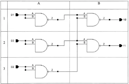
B
D0
gnd
Select0
mux_2to1
Dt
Figure
(4.6.2):
PIF
NAND
based
2-to-l Multiplexer
A 4-to-l
multiplexerimplementation
requiresjust
one gatewithlogic
depth
ofoneas seen
in Figure (4.6.3). Notice
that
select signalSelectl
andtwo
inputs
(D2
andD3)
areunused, thus
connectedto
ground.This
schematic showsthe
implementation
when
the
output ofthe
driving
gate ofthis
cellis
also connectedto
anothercellin
the
circuit.
If
the
incoming
signal'selectO'
is
notdriving
any
other gatebut just
one gatein
Selects
Mux_2to1
Figure
(4.6.3):
PIF
multiplexerbased
2-to-l Multiplexer
Figure
(4.6.4).
This
is
abetter
approachfor
delay
balancing
and powerdistribution.
PIF Multiplexer
based
circuit uses16
transistors to
implement
2-to-l
multiplexerincluding
the
inverters
neededby
the
selectlines,
but
it is
interesting
to
notethat
just
half
of
the
circuitis
actually
usedin
case ofthe
schematicin
Figure (4.6.3).
Thus,
4-to-l
multiplexer can
implement
more complexfunctions
easily
(less
complicated)
thanthe
D0
D1
Selects
D0
D1
D2
D3
S0
S1
-^Mux_2to1
Figure
(4.6.4):
PIF
multiplexerbased
2-to-l
Multiplexer
4.7: Performance
Assessment
The
circuits are simulatedusing
the
Cadence Spectra
simulatorwhichis
a part ofthe
Cadence
platform.The
inputs
ofthe target
circuits aredriven
by
inverters instead
ofinput
sourcesto
emulatethe
physical conditions evenbetter.
For
the samereasons,
theoutputs of
the target
circuitsdrive
aninverter.
The
performance of eachtarget
circuitis
evaluatedby
measuring
the
powerdissipation
and propagationdelay
for
a particularinput
combination.The
layout
areaofPIF
circuitsis
measuredfrom
the
cellsin
the
layout
library
designed
for
this
research.For
the
Standard
cellbased
circuitsthe
layout
areais
measured eitherdirectly
from layout
(2-to-1
Multiplexer)
orby
adding
the
layout
area ofthe
functional blocks
(8-to-l
Standard
cellFigure
(4.7.1)
showsthe
schematic arrangementfor
the
standard cellimplementation
of a2-to-l
multiplexer.The
symbolhas been
modifiedto
accommodatethe
VDD
andGND
pinswhich are usedin
powerdissipation
measurement.The
valuefor
VDD
is
2.5 V
for
IBM 0.25
umtechnology,
thus the
DC
sourceof2.5
V
is
used as seenin Figure (4.7.
1). A
resistor of1
Q is
connectedbetween
the
powersupply
in
the
circuitand
the
VDD
pin ofthe
2-to-l
multiplexer.Current
throughthis
resistoris
plottedduring
simulation and peak current and average current values are measured
for
powerdissipation
calculations.The
output ofthe
inverter
whichloads
the
2-to-l
multiplexeris
terminated
using
a20
fF
capacitor whichis
the
equivalentinput
capacitancefor
afanout
of2
in
the
0.25
umtechnology
used.TV2
4\Vdc=2.5 N
[
a
m ft a Ul w
a
oeiecw w
end
_D0_
Dl
SD
vdd
Mus<_Z1
sel 9nd
-ftMu>L2to1
CB
-l-c=20f
5nd
Figure
(4.7.
1):
Standard
cellbased
schematicfor
powerdissipation
measurementin
4.7.1: Power
dissipation
calculationPeak
power consumptionPpeak
=iPeakVDD
~(4.7.
1)
Average
power consumptionPav
=(l/T)Jp(t)
dt
=(VDD
/
T)JiDD(t)
dt
-(4.7.2)
where,
p(t)
is
the
instantaneous
power,
idd