This is a repository copy of Magnetic two-dimensional systems.
White Rose Research Online URL for this paper:
http://eprints.whiterose.ac.uk/117887/
Version: Accepted Version
Article:
Liu, Wenqing and Xu, Yongbing orcid.org/0000-0002-7823-0725 (2016) Magnetic
two-dimensional systems. CURRENT OPINION IN SOLID STATE. pp. 388-395. ISSN
1359-0286
https://doi.org/10.1016/j.cossms.2016.10.003
[email protected] https://eprints.whiterose.ac.uk/ Reuse
This article is distributed under the terms of the Creative Commons Attribution-NonCommercial-NoDerivs (CC BY-NC-ND) licence. This licence only allows you to download this work and share it with others as long as you credit the authors, but you can’t change the article in any way or use it commercially. More
information and the full terms of the licence here: https://creativecommons.org/licenses/
Takedown
If you consider content in White Rose Research Online to be in breach of UK law, please notify us by
1
Magnetic Two-Dimensional Systems
Wenqing Liu,1, 2 and Yongbing Xu1, 2, *
1 York-Nanjing Joint Center (YNJC) for Spintronics and Nanoengineering, School of Electronics
Science and Engineering, Nanjing University, Nanjing 210093, China
2 Spintronics and Nanodevice Laboratory, Department of Electronics, University of York, York
YO10 5DD, UK
* Author to whom correspondence should be addressed. Email: [email protected]
Abstract
Two-dimensional (2D) systems have considerably strengthened their position as one of the
premier candidates to become the key material for the proposed spintronics technology, in
which computational logic, communications, and information storage are all processed by
the electron spin. In this article, some of most representative 2D materials including
ferromagnetic metals (FMs) and diluted magnetic semiconductor (DMSs) in their thin film
form, magnetic topological insulators (TIs), magnetic graphene and magnetic transition
metal dichalcogenides (TMDs) are reviewed for their recent research progresses. FM thin
films have spontaneous magnetization and usually high Curie temperature (Tc), though this
can be strongly altered when bonded with semiconductors (SCs). DMS and magnetic TIs
have the advantage of easy integration with the existing SC-based technologies, but less
robust magnetism. Magnetic ordering in graphene and TMDs are even more fragile and
limited to cryogenic temperatures so far, but they particularly interesting topics due to the
desired long spin lifetime as well as the outstanding mechanical and optical properties of
2
1. Introduction
The possibility of providing ultimate logic bit by electronÕs spin rather than or in addition
to its charge has claimed exciting new horizons in physics, material science and electronic
engineering. For spin-electronics or spintronics purposes, the materials carrying out the
mission must be spin polarized, such as magnetic metals with the broken symmetry
between spin down and spin up states near the Fermi level (EF). Historically the spin
arrangement has long been investigated within the context of conventional FM and their
alloys, while the study of spin generation, relaxation, and spin-orbit coupling in
non-magnetic materials has taken off rather recently with the advent of spintronics and it is here
that many novel 2D materials and systems can find their greatest potential in both science
and technology.
The earliest studies of 2D magnetic phenomena can be tracked back to discussions
of the interfacial magnetism of FM/SC heterojunctions.[1-18] In this regard, a large portion
of the research work over the last two decades was stimulated by the idea of creating a spin
field effect transistor (SFET),[19] in which the transport of the electron spins is confined in
a high mobility 2D electron gas (2DEG) channel and can be manipulated by the application
of a gate voltage.An ideal spin-injected SC would demonstrate high spin polarization,
operate at room temperature (RT) and be both robust and easily fabricated for potential
high throughput needs. Various FM/SC heterostructure have been hotly investigated since
it was demonstrated that substantial spin accumulation and diffusion occurs at the FM/SC
interface.[20] The generation of high-spin-polarization current is essential for the SFET
concept and therefore the half metallic materials (such as Heusler alloys, Fe3O4, and CrO2)
have also been integrated into the hybrid systems.[21-23]Although an all electrical all
semiconductor spin field effect transistor has recently been demonstrated, all be it at 300
mK and requiring quantum ballistic point contacts;[24] hybrid systems with ferromagnetic
source and sink of spin and an easily gate tuned channel through a high mobility 2D
material may offer a route to the spin field effect transistor at room temperature.
Van der Waals materials such as graphene, layered TMDs, copper oxides, and iron
pnictides with properties dominated by their 2D structural units have become the new focus
of 2D magnetism research for the recent few years. The success of single-layer graphene
has shown that it is not only possible to exfoliate stable, single-atom or
single-polyhedral-thick 2D materials from bulk van der Waals solids, but also that these materials can exhibit
fascinating and technologically useful properties. In graphene's band structure, the linear
dispersion at the k point gives rise to novel physical phenomena, such as the anomalous
3 ÒDiracÓ physics. Stimulated by the rise of graphene, other 2D crystals including layered
hexagonal-boron nitride (h-BN) and TMDs were subsequently demonstrated.The more
recently discovered TIs, featured with an insulating bulk gap and gapless Dirac-like band
dispersion surface states, are new members of the 2D family.Unlike that of graphene, the
electron states of TIs surface are strongly spinÐorbit coupled and immune to
time-reversal-invariant disorders. Magnetism is not common for the elements consisting Van der Waals
2D materials; however, spin polarization in these materials can still be induced by defects,
edge states, magnetic dopants and/or via the proximity to an adjunct magnetic source etc..
Compared to FM, they generally have less robust magnetism, but significantly longer spin
lifetime or spin coherence length, which are eagerly desired in spintronics. Furthermore,
their capacity of integration with FM offers a promising direction toward the development
of hybrid devices that can perform logic, communications, and storage within the same
material technology.
In the reminder of this article, a selection of magnetic 2D systems will be
introduced, following their historical path of emergence. This includes FM and DMS in
their thin film form, magnetic TIs, magnetic graphene and magnetic TMDs, as illustrated in
Figure 1. The very recent advances of the study of these materials will be reviewed. This
article does in no way try to give a complete overview of the emerging 2D systems, as
many of them are still under fast developing till this day; neither is it intended to give deep
theoretical descriptions of why the many fascinating phenomena occur in them. The
purpose of this article is, instead, to present some of the most important findings of these
material systems and to highlight a few hotly debated topics of the contemporary magnetic
[image:4.595.185.407.539.690.2]2D systems research.
4
2. Ferromagnetic Metal Thin Films
As the simplest form of magnetic 2D system, transition metal thin films and their alloys
have been most thoroughly exploited in the history, as they are relatively easy to grow
epitaxially on III-V semiconductors (SCs) such as GaAs, InAs and InGaAs etc.. [1-18] In a
FM/SC heterojunction, the best opportunity for spin transport could only be achieved in the
absence of a magnetic dead layer at the interface. The atomic-scale interfacial
magnetization of the FM/SC is, in turn, closely linked with two general questions, namely
(i) how the magnetic ordering changes with reduced dimensionality and (ii) how the
magnetic ordering changes due to electronic bonding at the interface with the SC substrate.
In general, three factors are predominately responsible for the suppressed
magnetization of the FM/SC interfaces. One rises from the stacking of FM when epitaxially
deposited on SC. Bulk-like Co has its stable and metastable phase as hexagonal close
packed (hcp) and face center cubic (fcc), but can form into a body center cubic (bcc)
stacking by epitaxial growth on GaAs. The bcc Co/GaAs was firstly demonstrated by
Prinz[2, 4, 25] in 1985 and since then many experiments on Co/GaAs were reported with
inconsistency, making this issue rather complex.[1-6] Using high-resolution transmission
electron microscopy (TEM), Gu et al.[1] demonstrated hcp-structured epi-Co on GaAs and
Mangan et al.[2] observed the coexistence of bcc and hcp phases. Idzerda et al.[3]
confirmed the bcc structure of Co on GaAs(110) using extended x-ray absorption fine
structure and theory suggests that bcc Co is not a metastable phase but a forced structure
originating from imperfections.[4, 5] Calculations suggest bulk bcc Co can have a magnetic
moment aslarge as 1.7 µB/atom.[6] The tendency to form into bcc stacking, which doesnÕt
exist in nature, has also been found in epitaxial Ni thin films on GaAs. This was firstly
demonstrated by Tang et al.[7] as early as 1986 by growing Ni on GaAs(001) at RT and the
presence of bcc phase was observed up to 2.5 nm. This study was late on reproduced by X.
M. Jiang et al.,[8]who alternatively did the growth at 170 K and obtained a thicker bcc Ni,
i.e. 3.5 nm. The bcc Ni/GaAs(100) as having a Curie temperature (Tc) of 456 K and a
magnetic moment of 0.52 µB/atom, reveals a remarkably different electronic structure to
that of fcc Ni and crucially a positive cubic anisotropy of +4.0×10⁵ ergs/cm3, as opposed to −5.7×10⁴ ergs/cm3 for the naturally occurring fcc Ni.
Another possibility is associated with the detrimental interdiffusion between the
FM and the SC atoms. Theoretical calculations suggest a bulk bcc Co can carry a magnetic
momentas large as 1.7 µB/atom,[6, 9] while experimental reports are always below this
5 ferromagnetically dead layer associated with the formation of interfacial Co2GaAs for Co
thickness less than 3.4 monolayers (MLs) and an abrupt in-plane spin-reorientation
transition reorients the magnetization along the [001] direction at 7 ML. It should be noted
that all these boundaries discussed above are not absolute values but strongly depend on the
specific sample deposition conditions, such as the substrate configuration and the
temperature etc.. For example, passivating layers such as S and Sb have been used to
reduce the chemical interaction at the Co/GaAs interface and the latter gives a factor of 2.3
enhancement of the magnetic moment compared to the film deposited on bare GaAs(110)
substrate.[3] Characterized by x-ray photoelectron spectroscopy (XPS), the presence of the
As peak in the 6-nm Ni film reveals the occurrence of As diffusion into the Ni layer
destroying the magnetic properties of the fcc Ni film and leading to a 20% reduction of the
magnetization compared to the bulk value.[11] In the study of the evolution of interface
properties of the electrodeposited Ni film upon annealing, a significant increase of As
out-diffusion has been observed for annealing temperatures up to 623 K accompanying a rise in
the Schottky barrier height, which has been attributed to the Ni-Ga-As compound
formation.[12]
The third reason is the reduced thickness. It is well known that FM materials
follow the so-called island growth geometry at low coverage. In other words, FM atoms at
low thicknesses, typically less than a few MLs, may be too diffused for them to intensively
interact with one another. For example, many researchers have reported on high quality
epitaxial growth of Fe on GaAs, among which there exist the long lasting debate over the
presence of magnetic dead layer at the Fe/GaAs interface.[13]This detrimental effect used
to be attributed to the formation of antiferromagnetic Fe2As[14] and half-magnetized
Fe3Ga2xAsx in the vicinity of the interface, until Xu et al.[15] demonstrated the evolution of
the magnetic phase of Fe/GaAs corresponding to the growth morphology. This result was
further confirmed with unambiguous x-ray magnetic circularly dichroism (XMCD)
measurement of the Fe/GaAs(100) interface.[16]
Direct experimental demonstration of the magnetic state of epitaxial FM/SC
interface down to the atomic scale remains a nontrivial task, even up to this day, partially
due to the inaccessibility of the buried layer (referred to as FM2 hereafter) between the
upper layers (referred to as FM1 hereafter) and the substrate. One classical method of
resolving this problem is to engineer the FM1/FM2/SC superstructure, as shown in Figure
2.[16-18] Here, the FM2 layers, usually with one monolayer thickness, are epitaxially
deposited on the SC and then capped with a thick layer of FM1 (≠ FM2), which serves as
6 the FM2, providing it with a source of exchange interaction. Combined with the unique
element selectivity of XMCD, this structure allows direct observation of the interfacial
behavior of the bulk FM2 on the SC. Applying this approach to two model FM/SC systems,
namely Co/GaAs and Ni/GaAs, Liu et al.[18] observed a robust room temperature
magnetization of the interfacial Co, whilst that of the interfacial Ni was strongly
diminished down to 5 K due to hybridization of the Ni d(eg) and GaAs sp3 states. The validity of the selected method was confirmed by first-principles calculations, showing
only small deviations (<0.02and <0.07 µB/atom for Co/GaAs and Ni/GaAs, respectively)
compared to the real FM/SC interfaces. Their work also proved that the electronic structure
and magnetic ground state of the interfacial FM2 is not altered when the topmost FM2 is
replaced by FM1 and that this model is applicable for probing both magnetically active and
dead layers.
Figure 2. Demonstrate of the FM1/FM2/SC superstructure model. Upper row: Illustration of the FM1/FM2/SC structure (right) retrieving the FM2/SC structure (left). Lower row: the magnetic moment of Co/GaAs and Ni/GaAs interfaces versus distance along the (100) direction. The
[image:7.595.190.409.322.614.2]7
3. Diluted Magnetic Semiconductor Thin Films
One of the most useful aspects of SCs resides in their capacity to be doped with impurities,
by which the electrical properties of the SC can be tuned. This approach has been
developed to introduce magnetic ions into non-magnetic SCs to make them magnetic,
known as DMSs.[26] The concept behind it is that to transfer spin between similar
materials would be a simpler task than over a metal-SC interface due to the retained control
over band-gap engineering. The long established presence of spin filtering effects in these
SCs[27] and more recently observed properties for spontaneous[28, 29] or field
controlled[30, 31] magnetic ordering add to their viability in this field. The early
experimental efforts on the demonstration of DMSs started from II-VI (such as CdTe and
ZnSe) in which the transition metal ions (such as Mn) are easy to be doped to high
concentrations.[32] The fabrication of IIIÐV DMSs, on the other hand, was limited mostly
to (In,Mn)As,[28] (Ga,Mn)Sb,[33] and (Ga,As)Mn,[29, 34, 35] in which demonstrably
carrier-mediated ferromagnetism already persists.
While DMSs may offer opportunities of easy integration with conventional
SC-based devices, it is however a great challenge to improve the quality of DMS and in
particular to enhance their magnetism.[35-43] With the thickness down to nanometer scale,
these issues become even more sophisticated. For example, (Ga,As)Mn is a technological
important material due to its potential use in short-range optical communications, however,
whose highest Tc up to now is no more than 200 K even after combining efforts of heavy
Mn doping, nano-patterning, optimizing the growth conditions, and post-growth
annealing.[34, 35, 37, 44] RT ferromagnetism has been predicted and demonstrated in
magnetic oxide SCs such as Co- and Mn-doped ZnO, though debates exist on whether the
ferromagnetism obtained in DMS oxides is intrinsic or not.[38, 39]
In a magnetic bilayer system, the exchange coupling from a ferromagnetic layer
can induce a spin polarization in the nonmagnetic layer or enhance the TC in the other
magnetic layer with low ordering temperatures through the proximity effect. By such
approach, substantial increase of TC from 40 to 70 K due to the presence of a few
monolayers of Fe atop (Ga,Mn)As was obtained by Song et al. in a lateral spin injection
device.[40]The magnetic proximity effect persists to room temperature at Fe/(Ga,Mn)As
interfaces was reported by Maccherozzi et al.,[41, 42] who observed a significant induced
magnetic order in the (Ga,Mn)As layer that extends over more than 2 nm, as shown in
Figure 33. An antiparallel magnetic coupling between Fe and Mn, with ferromagnetic order
8 this system by Olejnik et al..[43] Altering the Fe induction layer with the high Tc half
metallic Heusler alloy Co2FeAl, Nie et al. demonstrate that a 1.36 nm thick (Ga,Mn)As
thin film remains ferromagnetically order up to 400 K. Unlike the antiferromagnetic
coupling in Fe/(Ga,Mn)As system, these authors observed a parallel alignment between the
[image:9.595.173.405.189.423.2]Fe, Co and the Mn in the Co2FeAl/(Ga,Mn)As system.
Figure 3. Demonstration of the enhanced magnetism of (Ga, Mn)As via proximity effect with Fe. (a) Spontaneous M(T) curves of Mn from a Fe/(Ga, Mn)As and a pure (Ga, Mn)As. (b) Sketch of the model for the Mn distribution ρ(x) and the fraction of ferromagnetic Mn δ(x) at RT. [41]Error!
Bookmark not defined.
4. Magnetic Topological Insulators
As a class of matter with newly discovered eccentric electronic phase, the spin-orbit
induced TIs have a rather short history but fast growing family.[45-47]Since they were
first theorized in 2005[48] and experimentally produced in 2006,[49] TIs, with their ability
to insulate on the inside and conduct on the outside, have presented new possibilities for
the future spintronics applications. Three-dimensional (3D) TIs feature novel phases of
quantum matter characterized by sharp changes in electronic structure at their very
surfaces, i.e. with insulating bulk band gap and gapless Dirac-like band dispersion surface
state (SS). Unlike the different electronic properties of the surface and the bulk universally
existing in all solids owing to the inevitable termination of periodic lattice structure when
9 strong spin-orbital coupling (SOC) and characterized by a Rashba spin texture.[50-52]
These low-dimensional conducting states are immune to localization as long as the disorder
potential is time-reversal-invariant and therefore have strong implications for the emerging
technologies such as dissipationless spin transport and quantum computing.[53, 54]
Breaking time-reversal-invariance by introducing magnetic perturbation, on the other hand,
reveals a complex phenomenology associated with an excitation gap of the surface
spectrum, resembling that of a massive Dirac fermion.[55, 56] Such a system with a
tunable gap promises rich exotic topological phenomena and would allow purely electric
control of the surface transport and magnetization.[45, 57, 58]
Two categories of route for introducing ferromagnetic order or breaking
time-reverse symmetry (TRS) in TIs have been developed. One route is to dope the TI host with
specific elements, by which ferromagnetism has been observed in Cr- and Mn-doped single
crystals of Sb2Te3,[59-61] Fe-, and Mn-doped single crystals of Bi2Te3,[62, 63] and Mn-
and Cr-doped thin films of Bi2Se3.[64, 65] However, for the electronic and magnetic
ground state of the magnetically doped TIs, evidence from the experimental observations
including magneto-transport measurements,[60] global magnetometry,[55]and core-level
spectroscopies[66-68]are so far inconclusive. Magnetic studies on epitaxial, Cr-doped
Bi2Se3 using superconducting quantum interference device - vibrating sample
magnetometer magnetometry (SQUID-VSM)[64] and polarized neutron reflectometry
(PNR)[68] universally reported a magnetic moment of no more than ∼2 µB/atom,
remarkably lower than the HundÕs rule of 3 µB/atom of substitutional Cr3+ on Bi sites.
According to the pioneering work by Haazen et al.,[64] the magnetic moment of Bi
2-xCrxSe3 decreases with increasing doping concentration and sharply drops beyond ∼10%.
This is well resembled by Liu et al.[69] using a combined approach of XMCD and density
function theory (DFT) calculation, as summarized in Figure 44. These authors found a
remarkable fraction of the (CrBi-CrI) 3+
antiferromagnetic dimers in the Bi2-xCrxSe3 for 0.02
< x < 0.40, which was neglected in previous studies. Significant mismatch also exists in
Mn- and Fe-doped Bi2Se3, who typically show global magnetic moments of ∼1.5 µB/atom
and ∼3µB/atom, while their HundÕs rule prediction is 5 µB/atom. It has been proposed that
in magnetic TIs, ferromagnetic moments can be developed not only through the s-d
exchange interaction such as in diluted magnetic semiconductors (DMSs),[34, 70-73] but
also through the van Vleck mechanism, by which magnetic ions are directly coupled
through the local valance elecrons.[47] Both types of mechanism have been observed
independently in Mn-doped Bi2(TeSe)3[74] and Cr-doped (BiSb)2Te3[75] thin films.
(TR-10 ARPES) has been performed to distinguish bulk and surface electron-phonon coupling of
the bare TI.[76] In the regard of magnetic TI, β-nuclear magnetic resonance (β-NMR)was
very recently used to depth-profile the electronic wavefunctions at topological
[image:11.595.173.416.164.437.2]surfaces.[77]
Figure 4. A summary of the experimentally measured and the DFT‐calculated dependence of (a) magnetic moment and (b) the fraction of the three predominant defects CrI3+, CrBi0, and (CrBi‐ CrI)
3+
, as a function of the chemical potential of Cr (μCr) in Bi2‐xCrxSe3.[69]
The other routine of making TIs magnetic is to engineer layered heterostructures,
where the SS of TIs experience the exchange interaction from an adjacent ferro- or ferri-
magnetic material. This route subsequently can be divided into two ways in terms of ferro-
or FM and ferro- or ferri- magnetic insulator (FMI) induction. Pioneering theoretical
work[78-80] suggests that suitable FMIs have the potential to achieve a strong and uniform
exchange coupling in contact with TIs without significant spin-dependent random
scattering of helical carriers on magnetic atoms. Progresses are made experimentally in
FMI/TI heterostructures including GdN/Bi2Se3 byKandala et al.,[81] EuS/Bi2Se3 by Yang
et al.,[82] andWei et al.,[83] respectively, although the effect observed is limited to low
temperature (< 22 K) due to the low TCof EuS. The interface magnetism of (anti-) FM/TI
heterostructures, such as Fe/Bi2Se3,[56, 84, 85]Co/Bi2Se3,[85]and Cr/Bi2Se3,[86] has also
11 ferromagnetism up to RT can be induced in Bi2-xMnxTe3 by a deposited Fe overlayer, as
shown in Figure 5. However, in the presence of a metallic layer, the nontrivial surface
states of the TI can be significantly altered due to their hybridization with the bulk states of
the (anti-) FM in contact. Besides, the metallic layer naturally short circuits the TI layer
and therefore fundamentally restrict the device design. Using high-Tc ferrimagnetic
insulator, [88] Liu et al.[89] demonstrated the magnetic proximity effect of Bi
2-xCrxSe3/Y3Fe5O12 and obtained a large (6.6 nm at 30 K) but fast decreasing penetration
depth compared to that of ordinary DMSs. This could indicate a novel mechanism for the
interaction between the ferromagnetic insulator and the nontrivial TIs surface and has
strong implications for the TI-based dissipationless electronic devices, as it no longer limits
[image:12.595.209.385.300.688.2]the ÒproximityÓ to short range.
12
5. Magnetic Graphene and Transition Metal Dichalcogenides
Since its successful synthesis by mechanical exfoliation from graphite in 2004, graphene
has attracted enormous attention in the community of physics, chemistry and materials
science.[90] As a prototypical two-dimensional quantum system, graphene displays a
combination of exceptional properties including large charge carrier mobility, high thermal
conductivity, strong mechanical strength, excellent optical characteristics, electrically
tuneable band gap, as well as the recently discovered long spin coherence length.[91-93]
The revolutionary nature of graphene makes it a prime candidate to become a key
material for the proposed spin transistors, in which the generation and tuning of
spin-polarized currents are prerequisites.[94-96] In pristine state, graphene exhibits no signs of
conventional spin-polarization and so far no experimental signature shows a ferromagnetic
phase of graphene. This gap is now filling up by combined efforts in multi-disciplinary
research. While ideal graphene is non-magnetic, many of its related materials and
nanostructures, either realized in practice or considered theoretically, have shown various
scenarios of magnetism. Pioneering works reveal that spin origin in graphene are defect,
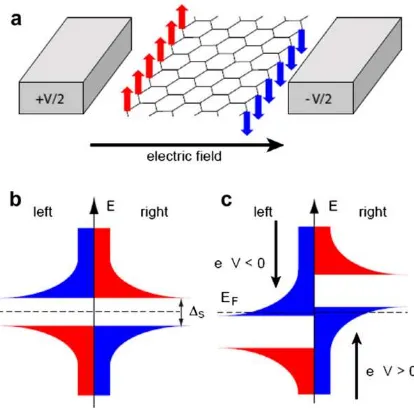
vacancy, and edge state where topological frustration of the p-bonds occurs. This was first
discussed by Son, Cohen and Louie, who showed that external electric fields can induce
half-metallicity Ð the coexistence of a metallic state for electrons with one spin orientation
and an insulating state for electrons with the opposite spin orientation, in the zigzag
graphene nano-ribbon (ZGNR), as shown in Figure 66.[97] Enoki et al. observed localized
spins in nano-graphite domains of activated carbon fibers and attributed the origin to the
[image:13.595.190.397.534.739.2]zigzag edges.[98]
13 across the nanoribbon, from left edge (spin‐up, red arrows) to right edge (spin‐ down, blue arrows). (b) Schematic representation of the spin‐resolved local density of states for the opposite edges at zero applied field. (c) Applied electric field breaks the symmetry for different spin types.[99]Error! Bookmark not defined.
Engineering FM/graphene heterojunction is one of the most promising avenues to
realise efficient spin injection into graphene and this was first achieved by Ohishi et al.
into ZGNRs at room temperature.[100] Fascinating properties of spin transport phenomena
have been presented in the Co/graphene system,[100, 101] though theoretical calculations
show that the atomic magnetic moment of Co can be reduced by more than 50% when
absorbed on graphene surface.[102] The magnetic moment of monolayer Fe is reduced but
still sizable when epitaxially deposited on graphene, and this in turn induces a spin
polarization in the carbon atoms.[103] The graphene-based FET has been demonstrated in
back gated devices on highly doped Si,[104] and the conductance of the top surface of such
structure can be modulated via gas exposure and top-back dual gates.[102]The spin valve
effect was also successfully demonstrated in NiFe/graphene/NiFe vertical structures and
the signal is enhanced when the number of graphene layers is doubled.[105] An inserted
graphene sheet can drastically improve the spin-injection efficiency from a ferromagnet
into silicon.[106] All these demonstrations indicate that the interaction of graphene with
FM surface plays a fundamental role in the related technological process, which has
renewed the interest of FM/SC heterojunctions, although the binding mechanism of the
FM/graphene interface is still far from a complete understanding.
Beyond graphene, the unique electronic and optical properties of TMDs are
establishing them as the next hotspot in 2D materials research. Despite the plethora of
reports on the electronic structure of the single layer TMDs it was only recently that their
magnetic features have been investigated. So far VS2 and VSe2 are the only 2D materials
with their magnetism confirmed in the pristine state.[99]For metal intercalated TMDs,
FexNbSe2 and CuxNbSe2 were proved to be magnetic.[107] In the case of MoS2 the
presence of magnetism was believed to be related to the defects (including structural
defects and/or adatoms and/or impurities).[108] The substitution of a S atom by atoms of
complete d band (Pd and Au) was found not to lead to magnetic polarization except for a
slight modification of the density of states near EF.[109] On the other hand, substitution of
a S atom by atoms with incomplete d band atoms (Fe, Mn and V) was found to induce spin
polarization and significant modification of the states near the band edges.[110] The
14 Very recently the effect on TMDÕs magnetism upon cation substitution with
magnetic impurities has became a key subject of interest. Mishra et al.[112] investigated
the long-range ferromagnetic ordering in fairly diluted Mn doped (less than 5%) MoS2,
MoSe2, MoTe2, and WS2 within the density functional theoryÐspin polarized generalized
gradient approximation and Hubbard- U (SGGA+U) parametrization. Cheng et al. [113]
studied the magnetism of the MoS2 monolayer doped with Mn, Fe, Co, Zn, Cd, and Hg and
found that the Fe and Co doping lead to antiferromagnetic ground states, while the doping
with Mn, Zn, Cd, and Hg lead to ferromagnetic ground states. Ramasubramaniam and
Naveh[114]compared the results for the exchange coupling coefficient among Mn dopants
in MoS2. They found noticeable differences only at the nearest neighbor dopant distances
and that ferromagnetic coupling between Mn dopants and antiferromagnetic spin
polarization between the Mn dopants and their fist nearest neighbor S anions. The very first
successful experimental demonstration of in situ doping of monolayer TMD is the
Mn-doped MoS2 included in Figure 7, reported by Zhang et al.[115] with the assistance of a
graphene buffer layer on sapphire. Unlike the theoretical studies which have focused on
doping of freestanding 2D materials, these authors show that the capacity of the
incorporation of magnetic dopants in TMD is highly dependent on the choice of the
substrate.
[image:15.595.139.448.432.585.2]15
6. Summary and Outlook
2D systems have become one of the most exciting new classes of materials due to the
wealth of exceptional physical properties that occur when charge, spin and heat transport
are confined to a plane. Their unique 2DEG-like behaviours not only enrich the world of
low-dimensional physics, but also provide a platform for transformative technical
innovations. In the pursuit for such goals, the intrinsic material properties (e.g. mobility,
anisotropy, conductivity etc.) are important indicators and the artificially synthetized
hybrid systems (e.g. multilayers, hybrid systems, and nano-structures etc.) are valuable
models for studying spin-dependent phenomena and could potentially be used as actual
components for an eventual spintronic device.
Among the four representative 2D systems reviewed in this article, FM thin films
have the topmost advantages of spontaneous magnetization and usually high Tc. Their
electronic and magnetic ground states have been intensively studied in the history, though
dramatic alterations occur when it comes to the FM/SC interface. Using FM as spin filters
also bring problems such as the well-known conductivity mismatch, based on the fact that a
FM metal has a conductivity typically several orders of magnitude larger than that of a SC,
which has limited the efficiency of spin injection. Interface engineering by means of
improved epitaxial deposition, interface doping, and buffer layer insertion etc. may
eliminate the undesired effects and further enhance the operation temperature of the
FM/SC-based spintronic devices. By contrast, DMS thin films naturally avoid the
difficulties of integration with conventional SC-based technologies; however great
challenges remain to improve their crystallinity and in particular their Tc. Magnetic
proximity effect is a promising pathway in this regard. Not only many DMS thin films, but
also the newly discovered TIs have shown their pronounced capacities with several high Tc
magnetic materials via proximity. The later even reveals an increasing penetration depth,
which are expected to free the proximity effect from short-range limit. Future work to
explore the tuning of the magnetization of TIs and its dependence on the band filling will
be of both great fundamental interest and practical merits.
2D materials like graphene and TMDs carry the desired long spin lifetime as well
as the outstanding mechanical and optical properties that FM, DMSs and TIs donÕt have. It
is rather unconventional to seek for magnetism from these Van der Waals materials, which
were believed nonmagnetic. Nevertheless research into magnetic graphene and magnetic
TMDs has rapidly taken off, though their magnetic signatures are so far fragile and limited
to cryogenic temperatures. This is because the origin of spin polarization of these materials
16 magnetic source etc.. Direct magnetic doping to high concentration and forming long-range
magnetic ordering persisting up to RT are still major obstacles for magnetic graphene and
TMDs. Investigations into the interplay between imbalanced spin states and the Dirac-like
band dispersions will lead to find experimental approaches to enhance the magnetism in 2D
17 References
[1] Gu E, Gester M, Hicken R, Daboo C, Tselepi M, Gray S, et al. Fourfold anisotropy and
structural behavior of epitaxial hcp Co/GaAs (001) thin films. Physical Review B.
1995;52:14704.
[2] Mangan M, Spanos G, Ambrose T, Prinz G. Transmission electron microscopy
investigation of Co thin films on GaAs (001). Applied physics letters. 1999;75:346-8.
[3] Idzerda Y, Elam W, Jonker B, Prinz G. Structure determination of metastable cobalt
films. Physical review letters. 1989;62:2480.
[4] Subramanian S, Liu X, Stamps R, Sooryakumar R, Prinz G. Magnetic anisotropies in
body-centered-cubic cobalt films. Physical Review B. 1995;52:10194.
[5] Izquierdo M, D‡vila M, Avila J, Ascolani H, Teodorescu C, Martin M, et al. Epitaxy
and magnetic properties of surfactant-mediated growth of bcc cobalt. Physical review
letters. 2005;94:187601.
[6] Bagayoko D, Ziegler A, Callaway J. Band structure of bcc cobalt. Physical Review B.
1983;27:7046.
[7] Moruzzi V, Marcus P, Schwarz K, Mohn P. Total energy surfaces in the MV plane for
bcc and fcc cobalt. Journal of magnetism and magnetic materials. 1986;54:955-6.
[8] Tian C, Qian D, Wu D, He R, Wu Y, Tang W, et al. Body-centered-cubic Ni and its
magnetic properties. Physical review letters. 2005;94:137210.
[9] Bland J, Bateson R, Riedi P, Graham R, Lauter H, Penfold J, et al. Magnetic properties
of bcc Co films. Journal of Applied Physics. 1991;69:4989-91.
[10] Monchesky T, Unguris J. Magnetic properties of CoÚ GaAs (110). Physical Review B.
2006;74:241301.
[11] Chen C, Idzerda Y, Lin H-J, Smith N, Meigs G, Chaban E, et al. Experimental
confirmation of the X-ray magnetic circular dichroism sum rules for iron and cobalt.
Physical review letters. 1995;75:152.
[12] Scheck C, Evans P, Zangari G, Schad R. Sharp ferromagnet/semiconductor interfaces
by electrodeposition of Ni thin films onto n-GaAs (001) substrates. Applied physics letters.
18 [13] Filipe A, Schuhl A, Galtier P. Structure and magnetism of the Fe/GaAs interface.
Applied physics letters. 1997;70:129-31.
[14] Prinz G, Rado G, Krebs J. Magnetic properties of single crystal {110} iron films
grown on GaAs by molecular beam epitaxy. Journal of Applied Physics. 1982;53:2087-91.
[15] Xu Y, Kernohan E, Freeland D, Ercole A, Tselepi M, Bland J. Evolution of the
ferromagnetic phase of ultrathin Fe films grown on GaAs (100)-4× 6. Physical Review B.
1998;58:890.
[16] Claydon J, Xu Y, Tselepi M, Bland J, Van der Laan G. Direct Observation of a
Bulklike Spin Moment at the F e/G a A s (100)− 4× 6 Interface. Physical review letters.
2004;93:037206.
[17] Giovanelli L, Panaccione G, Rossi G, Fabrizioli M, Tian C-S, Gastelois P, et al.
Layer-selective spectroscopy of FeÚ Ga As (001): Influence of the interface on the magnetic
properties. Physical Review B. 2005;72:045221.
[18] Liu W Q, Zhou Q H, Chen Q, Niu D X, Zhou Y, Xu Y B, Zhang R, Wang J L, and
van der Laan G. Probing the Buried Magnetic Interfaces. ACS App Mater Inter. 2015;00
11438p.
[19] Datta S, Das B. Electronic analog of the electro optic modulator. Applied Physics
Letters. 1990;56:665-7.
[20] Lou X, Adelmann C, Furis M, Crooker S, Palmstr¿m C, Crowell P. Electrical
detection of spin accumulation at a ferromagnet-semiconductor interface. Physical review
letters. 2006;96:176603.
[21] Nie S, Chin Y, Liu W, Tung J, Lu J, Lin H, et al. Ferromagnetic interfacial interaction
and the proximity effect in a Co2FeAl/(Ga, Mn) As bilayer. Physical review letters.
2013;111:027203.
[22] Liu W, Xu Y, Wong P, Maltby N, Li S, Wang X, et al. Spin and orbital moments of
nanoscale Fe3O4 epitaxial thin film on MgO/GaAs (100). Applied Physics Letters.
2014;104:142407.
[23] Liu W, Song M, Maltby N, Li S, Lin J, Samant M, et al. X-ray magnetic circular
dichroism study of epitaxial magnetite ultrathin film on MgO (100). Journal of Applied
19 [24] Hu Y, Zeng L, Minnich AJ, Dresselhaus MS, Chen G. Spectral mapping of thermal
conductivity through nanoscale ballistic transport. Nature nanotechnology. 2015;10:701-6.
[25] Prinz G. Stabilization of bcc Co via epitaxial growth on GaAs. Physical Review
Letters. 1985;54:1051.
[26] Ohno H. Making nonmagnetic semiconductors ferromagnetic. Science.
1998;281:951-6.
[27] Esaki L, Stiles P, Von Molnar S. Magnetointernal field emission in junctions of
magnetic insulators. Physical Review Letters. 1967;19:852.
[28] Munekata H, Ohno H, Von Molnar S, SegmŸller A, Chang L, Esaki L. Diluted
magnetic III-V semiconductors. Physical Review Letters. 1989;63:1849.
[29] Ohno H, Shen A, Matsukura F, Oiwa A, Endo A, Katsumoto S, et al. (Ga, Mn) As: a
new diluted magnetic semiconductor based on GaAs. Applied Physics Letters.
1996;69:363-5.
[30] Ohno H, Chiba D, Matsukura F, Omiya T, Abe E, Dietl T, et al. Electric-field control
of ferromagnetism. Nature. 2000;408:944-6.
[31] Matsukura F, Chiba D, Omiya T, Abe E, Dietl T, Ohno Y, et al. Control of
ferromagnetism in field-effect transistor of a magnetic semiconductor. Physica E:
Low-dimensional Systems and Nanostructures. 2002;12:351-5.
[32] Hovel HJ. Semiconductor and semimetals, Vol. 11. Solar cells. 1975:24.
[33] Adhikari T, Basu S. Electrical properties of gallium manganese antimonide: a new
diluted magnetic semiconductor. Japanese journal of applied physics. 1994;33:4581.
[34] Edmonds K, van der Laan G, Farley N, Campion R, Gallagher B, Foxon C, et al.
Magnetic linear dichroism in the angular dependence of core-level photoemission from
(Ga, Mn) As using hard X rays. Physical review letters. 2011;107:197601.
[35] Wang M, Campion R, Rushforth A, Edmonds K, Foxon C, Gallagher B. Achieving
high curie temperature in (Ga, Mn)As. Applied Physics Letters. 2008;93:132103.
[36] Edmonds K, Wang K, Campion R, Neumann A, Farley N, Gallagher B, et al. High
Curie temperature GaMnAs obtained by resistance-monitored annealing. applied Physics
20 [37] MacDonald A, Schiffer P, Samarth N. Ferromagnetic semiconductors: moving beyond
(Ga, Mn)As. Nature materials. 2005;4:195-202.
[38] Coey J. Dilute magnetic oxides. Current Opinion in Solid State and Materials Science.
2006;10:83-92.
[39] Dietl T. A ten-year perspective on dilute magnetic semiconductors and oxides. Nature
materials. 2010;9:965-74.
[40] Song C, Sperl M, Utz M, Ciorga M, Woltersdorf G, Schuh D, et al. Proximity induced
enhancement of the Curie temperature in hybrid spin injection devices. Physical review
letters. 2011;107:056601.
[41] Maccherozzi F, Sperl M, Panaccione G, Min‡r J, Polesya S, Ebert H, et al. Evidence
for a magnetic proximity effect up to room temperature at Fe/(Ga, Mn) As interfaces.
Physical review letters. 2008;101:267201.
[42] Sperl M, Maccherozzi F, Borgatti F, Verna A, Rossi G, Soda M, et al. Identifying the
character of ferromagnetic Mn in epitaxial Fe/(Ga, Mn) As heterostructures. Physical
Review B. 2010;81:035211.
[43] Olejnik K, Wadley P, Haigh J, Edmonds K, Campion R, Rushforth A, et al. Exchange
bias in a ferromagnetic semiconductor induced by a ferromagnetic metal: Fe/(Ga, Mn) As
bilayer films studied by XMCD measurements and SQUID magnetometry. Physical
Review B. 2010;81:104402.
[44] Edmonds K, Wang K, Campion R, Neumann A, Farley N, Gallagher B, et al. High
Curie temperature GaMnAs obtained by resistance-monitored annealing. arXiv preprint
cond-mat/0209554. 2002.
[45] Chang C-Z, Zhang J, Feng X, Shen J, Zhang Z, Guo M, et al. Experimental
observation of the quantum anomalous Hall effect in a magnetic topological insulator.
Science. 2013;340:167-70.
[46] Liu C-X, Qi X-L, Dai X, Fang Z, Zhang S-C. Quantum anomalous Hall effect in Hg1−
yMnyTe quantum wells. Physical review letters. 2008;101:146802.
[47] Yu R, Zhang W, Zhang H-J, Zhang S-C, Dai X, Fang Z. Quantized anomalous Hall
21 [48] Kane CL, Mele EJ. Z 2 topological order and the quantum spin Hall effect. Physical
review letters. 2005;95:146802.
[49] Bernevig BA, Hughes TL, Zhang S-C. Quantum spin Hall effect and topological phase
transition in HgTe quantum wells. Science. 2006;314:1757-61.
[50] Hasan MZ, Kane CL. Colloquium: topological insulators. Reviews of Modern
Physics. 2010;82:3045.
[51] Moore JE. The birth of topological insulators. Nature. 2010;464:194-8.
[52] Hsieh D, Xia Y, Qian D, Wray L, Dil J, Meier F, et al. A tunable topological insulator
in the spin helical Dirac transport regime. Nature. 2009;460:1101-5.
[53] Roushan P, Seo J, Parker CV, Hor Y, Hsieh D, Qian D, et al. Topological surface
states protected from backscattering by chiral spin texture. Nature. 2009;460:1106-9.
[54] Fu L, Kane CL, Mele EJ. Topological insulators in three dimensions. Physical Review
Letters. 2007;98:106803.
[55] Chen Y, Chu J-H, Analytis J, Liu Z, Igarashi K, Kuo H-H, et al. Massive Dirac
fermion on the surface of a magnetically doped topological insulator. Science.
2010;329:659-62.
[56] Wray LA, Xu S-Y, Xia Y, Hsieh D, Fedorov AV, San Hor Y, et al. A topological
insulator surface under strong Coulomb, magnetic and disorder perturbations. Nature
Physics. 2011;7:32-7.
[57] Garate I, Franz M. Inverse spin-galvanic effect in the interface between a topological
insulator and a ferromagnet. Physical review letters. 2010;104:146802.
[58] Yokoyama T, Tanaka Y, Nagaosa N. Anomalous magnetoresistance of a
two-dimensional ferromagnet/ferromagnet junction on the surface of a topological insulator.
Physical Review B. 2010;81:121401.
[59] Dyck J, Drašar Č, LoštÕ‡k P, Uher C. Low-temperature ferromagnetic properties of the
diluted magnetic semiconductor Sb2−xCrxTe3. Physical Review B. 2005;71:115214.
[60] Kou X, He L, Lang M, Fan Y, Wong K, Jiang Y, et al. Manipulating surface-related
ferromagnetism in modulation-doped topological insulators. Nano letters.
22 [61] Dyck JS, H‡jek P, LoštÕ‡k P, Uher C. Diluted magnetic semiconductors based on Sb2−
xVxTe3(0.01<~ x<~ 0. 0 3). Physical Review B. 2002;65:115212.
[62] Hor Y, Roushan P, Beidenkopf H, Seo J, Qu D, Checkelsky J, et al. Development of
ferromagnetism in the doped topological insulator Bi2−xMnxTe3. Physical Review B.
2010;81:195203.
[63] Kulbachinskii V, Kaminskii AY, Kindo K, Narumi Y, Suga K, Lostak P, et al.
Ferromagnetism in new diluted magnetic semiconductor Bi2−xFexTe3. Physica B:
Condensed Matter. 2002;311:292-7.
[64] Haazen P, Lalo‘ J-B, Nummy T, Swagten H, Jarillo-Herrero P, Heiman D, et al.
Ferromagnetism in thin-film Cr-doped topological insulator Bi2Se3. Applied Physics
Letters. 2012;100:082404.
[65] Kou X, Lang M, Fan Y, Jiang Y, Nie T, Zhang J, et al. Interplay between different
magnetisms in Cr-doped topological insulators. ACS nano. 2013;7:9205-12.
[66] Figueroa A, van der Laan G, Collins-McIntyre L, Zhang S-L, Baker A, Harrison S, et
al. Magnetic Cr doping of Bi2Se3: Evidence for divalent Cr from x-ray spectroscopy.
Physical Review B. 2014;90:134402.
[67] Collins-McIntyre L, Watson M, Baker A, Zhang S, Coldea A, Harrison S, et al. X-ray
magnetic spectroscopy of MBE-grown Mn-doped Bi2Se3 thin films. AIP Advances.
2014;4:127136.
[68] Watson M, Collins-McIntyre L, Shelford L, Prabhakaran D, Speller S, Mousavi T, et
al. Study of the structural, electric and magnetic properties of Mn-doped Bi2Te3 single
crystals. New Journal of Physics. 2013;15:103016.
[69] Liu W, West D, He L, Xu Y, Liu J, Wang K, et al. Atomic-Scale Magnetism of
Cr-Doped Bi2Se3 Thin Film Topological Insulators. ACS nano. 2015;9:10237-43.
[70] Ruderman MA, Kittel C. Indirect exchange coupling of nuclear magnetic moments by
conduction electrons. Physical Review. 1954;96:99.
[71] Yosida K. Magnetic properties of Cu-Mn alloys. Physical Review. 1957;106:893.
[72] Jungwirth T, Sinova J, Mašek J, Kučera J, MacDonald A. Theory of ferromagnetic
23 [73] Hong NH, Sakai J, Poirot N, BrizŽ V. Room-temperature ferromagnetism observed in
undoped semiconducting and insulating oxide thin films. Physical Review B.
2006;73:132404.
[74] Checkelsky JG, Ye J, Onose Y, Iwasa Y, Tokura Y. Dirac-fermion-mediated
ferromagnetism in a topological insulator. Nature Physics. 2012;8:729-33.
[75] Chang CZ, Zhang J, Liu M, Zhang Z, Feng X, Li K, et al. Thin Films of Magnetically
Doped Topological Insulator with Carrier Independent Long Range Ferromagnetic
Order. Advanced materials. 2013;25:1065-70.
[76] Sobota JA, Yang S-L, Leuenberger D, Kemper AF, Analytis JG, Fisher IR, et al.
Distinguishing bulk and surface electron-phonon coupling in the topological insulator
Bi2Se3 using time-resolved photoemission spectroscopy. Physical review letters.
2014;113:157401.
[77] Koumoulis D, Morris GD, He L, Kou X, King D, Wang D, et al. Nanoscale β-nuclear
magnetic resonance depth imaging of topological insulators. Proceedings of the National
Academy of Sciences. 2015;112:E3645-E50.
[78] Luo W, Qi X-L. Massive Dirac surface states in topological insulator/magnetic
insulator heterostructures. Physical Review B. 2013;87:085431.
[79] Eremeev S, Men'shov V, Tugushev V, Echenique PM, Chulkov EV. Magnetic
proximity effect at the three-dimensional topological insulator/magnetic insulator interface.
Physical Review B. 2013;88:144430.
[80] Men'shov V, Tugushev V, Eremeev S, Echenique PM, Chulkov EV. Magnetic
proximity effect in the three-dimensional topological insulator/ferromagnetic insulator
heterostructure. Physical Review B. 2013;88:224401.
[81] Kandala A, Richardella A, Rench D, Zhang D, Flanagan T, Samarth N. Growth and
characterization of hybrid insulating ferromagnet-topological insulator heterostructure
devices. Applied Physics Letters. 2013;103:202409.
[82] Yang QI, Dolev M, Zhang L, Zhao J, Fried AD, Schemm E, et al. Emerging weak
localization effects on a topological insulatorÐinsulating ferromagnet (Bi2Se3-EuS)
24 [83] Wei P, Katmis F, Assaf BA, Steinberg H, Jarillo-Herrero P, Heiman D, et al.
Exchange-coupling-induced symmetry breaking in topological insulators. Physical review
letters. 2013;110:186807.
[84] Li J, Wang Z, Tan A, Glans P-A, Arenholz E, Hwang C, et al. Magnetic dead layer at
the interface between a Co film and the topological insulator Bi2Se3. Physical Review B.
2012;86:054430.
[85] West D, Sun Y, Zhang S, Zhang T, Ma X, Cheng P, et al. Identification of magnetic
dopants on the surfaces of topological insulators: Experiment and theory for Fe on Bi2Te3
(111). Physical Review B. 2012;85:081305.
[86] Zhao X, Dai X-Q, Zhao B, Wang N, Ji Y-Y. Cr adsorption induced magnetism in
Bi2Se3 film by proximity effects. Physica E: Low-dimensional Systems and
Nanostructures. 2014;55:9-12.
[87] Vobornik I, Panaccione G, Fujii J, Zhu Z-H, Offi F, Salles BR, et al. Observation of
Distinct Bulk and Surface Chemical Environments in a Topological Insulator under
Magnetic Doping. The Journal of Physical Chemistry C. 2014;118:12333-9.
[88] Lang M, Montazeri M, Onbasli MC, Kou X, Fan Y, Upadhyaya P, et al. Proximity
induced high-temperature magnetic order in topological insulator-ferrimagnetic insulator
heterostructure. Nano letters. 2014;14:3459-65.
[89] Liu W, He L, Xu Y, Murata K, Onbasli MC, Lang M, et al. Enhancing magnetic
ordering in Cr-doped Bi2Se3 using high-TC ferrimagnetic insulator. Nano letters.
2014;15:764-9.
[90] Geim AK, Novoselov KS. The rise of graphene. Nature materials. 2007;6:183-91.
[91] Min H, Hill J, Sinitsyn NA, Sahu B, Kleinman L, MacDonald AH. Intrinsic and
Rashba spin-orbit interactions in graphene sheets. Physical Review B. 2006;74:165310.
[92] Tombros N, Jozsa C, Popinciuc M, Jonkman HT, Van Wees BJ. Electronic spin
transport and spin precession in single graphene layers at room temperature. Nature.
2007;448:571-4.
25 [94] Li X, Wang X, Zhang L, Lee S, Dai H. Chemically derived, ultrasmooth graphene
nanoribbon semiconductors. Science. 2008;319:1229-32.
[95] Wang X, Ouyang Y, Li X, Wang H, Guo J, Dai H. Room-temperature
all-semiconducting sub-10-nm graphene nanoribbon field-effect transistors. Physical review
letters. 2008;100:206803.
[96] Prinz GA. Magnetoelectronics. Science. 1998;282:1660-3.
[97] Huang B, Yan Q-m, Li Z-y, Duan W-h. Towards graphene nanoribbon-based
electronics. Frontiers of Physics in China. 2009;4:269-79.
[98] Shibayama Y, Sato H, Enoki T, Endo M. Disordered magnetism at the metal-insulator
threshold in nano-graphite-based carbon materials. Physical review letters. 2000;84:1744.
[99] Ma Y, Dai Y, Guo M, Niu C, Zhu Y, Huang B. Evidence of the existence of
magnetism in pristine VX2 monolayers (X= S, Se) and their strain-induced tunable
magnetic properties. ACS nano. 2012;6:1695-701.
[100] Ohishi M, Shiraishi M, Nouchi R, Nozaki T, Shinjo T, Suzuki Y. Spin injection into
a graphene thin film at room temperature. Japanese Journal of Applied Physics.
2007;46:L605.
[101] Han W, Kawakami RK. Spin relaxation in single-layer and bilayer graphene.
Physical review letters. 2011;107:047207.
[102] Ando K, Saitoh E. Inverse spin-Hall effect in palladium at room temperature. Journal
of Applied Physics. 2010;108:113925.
[103] Liu W, Wang W, Wang J, Wang F, Lu C, Jin F, et al. Atomic-Scale Interfacial
Magnetism in Fe/Graphene Heterojunction. Scientific reports. 2015;5.
[104] Novoselov KS, Geim AK, Morozov S, Jiang D, Zhang Y, Dubonos Sa, et al. Electric
field effect in atomically thin carbon films. Science. 2004;306:666-9.
[105] Iqbal MZ, Iqbal MW, Lee JH, Kim YS, Chun S-H, Eom J. Spin valve effect of
NiFe/graphene/NiFe junctions. Nano Research. 2013;6:373-80.
[106] Van't Erve O, Friedman A, Cobas E, Li C, Robinson J, Jonker B. Low-resistance spin
injection into silicon using graphene tunnel barriers. Nature nanotechnology.
26 [107] Koh Y, Cho S, Lee J, Yang L-X, Zhang Y, He C, et al. Growth and Electronic
Structure Studies of Metal Intercalated Transition Metal Dichalcogenides MxNbSe2 (M: Fe
and Cu). Japanese Journal of Applied Physics. 2013;52:10MC5.
[108] Ataca C, Ciraci S. Functionalization of single-layer MoS2 honeycomb structures. The
Journal of Physical Chemistry C. 2011;115:13303-11.
[109] Fuhr JD, Saœl A, Sofo JO. Scanning Tunneling Microscopy Chemical Signature of
Point Defects on the MoS2 (0001) Surface. Physical review letters. 2004;92:026802.
[110] Andriotis AN, Menon M. Tunable magnetic properties of transition metal doped
MoS2. Physical Review B. 2014;90:125304.
[111] He J, Wu K, Sa R, Li Q, Wei Y. Magnetic properties of nonmetal atoms absorbed
MoS2 monolayers. Applied Physics Letters. 2010;96:082504.
[112] Mishra R, Zhou W, Pennycook SJ, Pantelides ST, Idrobo J-C. Long-range
ferromagnetic ordering in manganese-doped two-dimensional dichalcogenides. Physical
Review B. 2013;88:144409.
[113] Cheng Y, Zhu Z, Mi W, Guo Z, Schwingenschlšgl U. Prediction of two-dimensional
diluted magnetic semiconductors: doped monolayer MoS2 systems. Physical Review B.
2013;87:100401.
[114] Ramasubramaniam A, Naveh D. Mn-doped monolayer MoS2: an atomically thin
dilute magnetic semiconductor. Physical Review B. 2013;87:195201.
[115] Zhang K, Feng S, Wang J, Azcatl A, Lu N, Addou R, et al. Manganese doping of

![Figure 2. Demonstrate of the FM1/FM2/SC superstructure model. Upper row: Illustration of the FM1/FM2/SC structure (right) retrieving the FM2/SC structure (left). Lower row: the magnetic moment of Co/GaAs and Ni/GaAs interfaces versus distance along the (100) direction. The dashed lines indicate the interfacial or the FM2 region, where the magnetic ground state of the interfacial FM2 is not altered when the topmost FM2 is replaced by FM1.[18]](https://thumb-us.123doks.com/thumbv2/123dok_us/7861158.180022/7.595.190.409.322.614/demonstrate-superstructure-illustration-structure-retrieving-interfaces-interfacial-interfacial.webp)
![Figure 3. Demonstration of the enhanced magnetism of (Ga, Mn)As via proximity effect with Fe. (a) Spontaneous M(T) curves of Mn from a Fe/(Ga, Mn)As and a pure (Ga, Mn)As. (b) Sketch of the model for the Mn distribution ρ(x) and the fraction of ferromagnetic Mn δ(x) at RT. [41]Error! Bookmark not defined.](https://thumb-us.123doks.com/thumbv2/123dok_us/7861158.180022/9.595.173.405.189.423/demonstration-magnetism-proximity-spontaneous-distribution-fraction-ferromagnetic-bookmark.webp)
![Figure 4. A summary of the experimentally measured and the DFT‐calculated dependence of (a) magnetic moment and (b) the fraction of the three predominant defects CrI3+, CrBi0, and (CrBi‐CrI)3+, as a function of the chemical potential of Cr (μCr) in Bi2‐xCrxSe3.[69]](https://thumb-us.123doks.com/thumbv2/123dok_us/7861158.180022/11.595.173.416.164.437/experimentally-calculated-dependence-magnetic-fraction-predominant-function-potential.webp)
![Figure 5. The antiferromagnetically coupled hysteresis loops of Mn and Fe, respectively, from the Fe/ Bi2‐xMnxTe3 bilayer from 22 K to 273 K.[87]](https://thumb-us.123doks.com/thumbv2/123dok_us/7861158.180022/12.595.209.385.300.688/figure-antiferromagnetically-coupled-hysteresis-loops-respectively-xmnxte-bilayer.webp)
![Figure 7. Experimental demonstration of Mn‐doped MoS2. Left: TEM image of Mn‐doped MoS2. Right: Two‐terminal conductance versus back gate voltage measurements indicating that Mn‐doping leads to an increase in the density of states in the bandgap of the MoS2 and thus lower saturation conductance.[115]](https://thumb-us.123doks.com/thumbv2/123dok_us/7861158.180022/15.595.139.448.432.585/experimental-demonstration-conductance-measurements-indicating-increase-saturation-conductance.webp)
