Abstract: This paper deals with the mitigation of voltage related PQ issues by using three phase neutral clamped VSI topology is used to realize the DVR and the design of DVR for the selection of suitable interface inductor, DC capacitor storage series resistance and the capacitance. Here three-phase four wire DVR with modified switching band controller topology is proposed, which overcome the frequent band violation, poor controllability and heavy filter currents, and compared to three-phase four wire DVR with conventional filter topology. The compensation capability of the proposed topology is analyzed based on simulation studies and corresponding results are compared with different switching control strategies. The consequent merits and demerits switching loss in VSI, ripple in compensated load voltages and error between reference injected voltages and actual injected voltages in different switching control strategies are discussed.
Keywords: Dynamic Voltage Restorer (DVR), Neutral Clamped VSI,Switching Band Controller, Synchronous Reference Theory (SRF) and Power Quality (PQ).
I. INTRODUCTION
The demand for electricity is booming due to growth in population and economy in the last decade. The quality and reliable power are essential for sustainable development of any country. Now a day‟s a large number of Renewable Energy Sources (RES) are integrated to the distribution the grid to achieve reliable and to meet the present electrical energy demand. However, the interaction of RES requires the use of power the electronic converters. However, they introduce distortion in Voltage (V) and Current (I), which leads to many PQ issues [1],[2]. Moreover, other PQ issues like voltage unbalance and voltage sag/swell are arising due to various power system faults, large single phase loads like traction loads, induction furnace loads and connection /disconnection of heavy loads in the distribution grid. Non-linear loads, for example, control hardware gear including Adjustable Speed Drives (ASD), Switched Mode Power Supplies (SMPS), and data processing equipment type of loads, starting of large motors, lightning and switching surges, etc., causes, harmonics in distribution grid [3]. The adverse effects with these PQ issues are excessive neutral currents, overheating of the electrical Equipment, voltage distortions leading to malfunctioning of the relays, increased power losses in the distribution systems and interference with
Revised Manuscript Received on November 06, 2019.
Dr Vasudeva Naidu, Electrical department, Matrusri Engineering College, Hyderabad, India. Email: [email protected]
Dr Srinivas Sura, Electrical department, GITAM, Vishakhapatnam, India. Email: [email protected]
Prasad Bolla, Electrical department, GITAM, Hyderabad, India Email: [email protected]
the communication systems [4]. Hence, there is a need for corrective measures to achieve quality and reliable power. There are several approaches proposed by the researchers for mitigating the PQ problems in the existing literature. Earlier researcher‟s proposed passive filters consisting of inductor and capacitors tuned for a particular frequency, are used to reduce these power quality problems, but these filters have the limitations like bulky in size, involve in series and parallel resonance, need for the high rating and require proper reactive power coordination. To overcome the above mentioned problems, active power filters are introduced in [5]-[8]. They are also called custom power devices (CPDs) when these are utilized in power distribution systems [3]. Recently many researchers have been proposed CPDs overcome power quality issues in distribution systems. The custom power devices include D-STATCOM, DVR and UPQC have been realized using power electronic converters [9]. However, control of these power electronic converters is a key concern for mitigating the PQ issues in distribution systems.
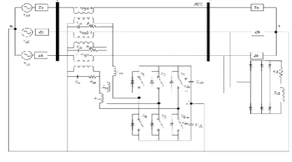
In present era the major power quality issue facing industries, local customers are voltage sag, voltage swell, interruptions etc., so in this paper is designed the dynamic voltage restorer (DVR) to compensate the voltage related issues in load end or at PCC. The design of DVR the primary consideration is selection of VSI topology, Various VSI topologies are used for mitigate voltage related problems at the PCC like three phase 3-wire VSI topology, H-bridge VSI Topology, three phase 4-wire VSI topology etc., but in this paper designed neutral clamped VSI topology based DVR is shown Fig.1. Here VSI consist of switches 1, 3, 5 in upper limb and 4, 2, 6 in lower limb with diode in parallel to each switch. Two identical D.C. Storage capacitors (common DC-link) are connected in parallel to VSI. By taking energy stored in DC link each leg of VSI is independently controlled [10]-[12]. The second important aspect in design of DVR is the selection of suitable coupling transformer, it can experience saturation during the transient period after a voltage sag starts. For preventing this, normally the value of flux taken is twice that of steady state limit. The DVR coupling transformer performs two important functions: voltage boost and electrical isolation. The third consideration in design of switching band filter circuit which consist of interfacing inductor and the passive capacitor (Cse) finally the selection of reference DC link voltage values is also essential [13]-[14].This method has a major drawback i.e reverse dc voltage is applied using control algorithim, which leads to increase in switching loss, and which in turn injects ripples into the injected voltage. These ripples reduces the system performance.
Performance Analysis of Three-Phase DVR with
Modified Switching Band Controller
Hence in this chapter three-phase four wire DVR with modified switching band controller topology is proposed, which over comes the switching losses, poor controllability and improve the system performance. The DVR consist of switching band filter hence the performance of depends on the values of filter components. The simulation studies carried out and the compensation capability of proposed method with different switching control strategies, merits and demerits, switching loss in VSI, ripple in compensated load voltages and error between reference injected voltages and actual injected voltages are discussed.
II. SYSTEMREPRESENTATION
Schematic of conventional three phase three leg-four wire DVR topology is shown Fig.1.This topology consists of voltage source inverter (VSI) connected in series to load at the PCC through injection transformer, interface filter (interface inductor ( ) and capacitor ( ). The purpose of interfacing filter is to shape inject voltages while tracking the reference injected voltages. Here , , represents the instantaneous phase voltages at the PCC, which may be distorted because of faults that can exist in the system are single line-to-ground fault, double line-to-ground, line-to-line
fault and three-phase fault. The injected
voltages , represents the actual injected
voltages obtained using hysteresis control
technique, , , represents the source currents and , , represents the load currents. The capacitance is the dc storage capacitor used for maintaining the input voltage of VSI at reference value of . However,
[image:2.595.308.547.179.282.2]instantaneous voltage across is denote as in following text.
Fig.1 Schematic diagram of conventional three phase four wire DVR topology
A. Different Operations of DVR In-Phase Boosting Technique:
The phasor diagram of the DVR compensated distributed system through in-phase boosting technique is shown in Fig. 2. The load voltage is 1
1 l
V before occurrence of sag and the load draws a current 1
1
l
I at a power factor angle . The source current 1
1 s
I is in phase with the load voltageVl11. It can be observed from Fig.2 that the terminal voltage will be
1 2
t
V with phase jump
due to the sag in the system. In DVR through in-phase boosting operation during balanced sag, the series active power filter (SEAPF or DVR) injects voltage in phase with source current and voltage sag to achieve nominal voltage. In case of unbalanced voltage sag with phase jumps, by in-phase boosting operation nominal load voltage can be attained but phase jumps are not eliminated. Hence, in-phaseboosting operation is not applicable for mitigating the negative and zero sequence sag voltages. Hence, first the negative sequence voltage, 1
2
t
V and zero sequence voltage
10 2
t
V of the terminal voltage sag 1 2
t
V should be mitigated to make it balanced sag. After mitigating 1
2
t
V and 10 2
t
V , DVR
also injects 1
inj
V in phase with the source current 1 2
s I to
achieve the nominal load voltage 1
inj
V with respect to 1 2
t V
labelled as X which is shown in Fig.2. Therefore, real power is injected into the system by DVR in order to achieve 1
2
l V .
Fig. 2. Phasor diagram for DVR through in-phase boosting operation
Pre-Sag Supply Voltage Boosting Technique
In this method, the series injected voltage is vector difference between the presage voltage and the sag voltage (i.e.,
1
inj
V 1 1
1 2
t t
V V
), which is shown in Fig.3. This method of operation is called as DVR-presag. Here, the DVR injects both real and reactive power. In all the above methods, except pre-sag supply voltage boosting operation, the mitigation of voltage sag with phase jumps is with respect to positive sequence voltage sag( 1
2
t
V ). The DVR require positive sequence voltage components only but in above methods it inject the negative sequence voltage ( 1
2
t
V ), zero sequence
voltage ( 10 2
t
V ) and along with 1
inj
V . Hence the VA loading
[image:2.595.68.277.457.573.2]increase.
Fig.3. Phasor diagram for DVR- presag operation. B. Control Theory for Generation of Reference
Quantities in DVR
The DVR has two important tasks first one is the generation of reference injecting voltages and secondly comparing these voltages with that of actual voltages generated by voltage source inverter (VSI).
C. Generation injected voltages by using synchronous reference frame (SRF) method.
Synchronous Reference Frame (SRF) theory:
This theory discussed is used to generate reference compensating voltages for DVR. Here it is used to generate reference injected voltage for DVR. By using park transformation the three phase instantaneous voltages in abc
reference frame are transferred to dq0 rotating reference, and the expressions of voltages as
0
cos cos 2 3 cos 2 3
2
sin sin 2 3 sin 2 3
3
1 2 1 2 1 2
sq sa
sd sb
s sc
v v
v v
v v
(1)
0
0 t
t t dt
(2)_ _
dqo s dqo abc s abc
v
T
v
(3)Now, at , the frequency component of source voltages include both oscillating components (
v
sd andv
sq), average components (vsd andvsq) and under unbalanced sourcevoltage with harmonics. Switching loss of VSI ( vloss ) component should be added to vsd obtain total axis
reference injected voltages. In oscillating components _q s
v
having source voltage negative-sequence components and harmonic under distorted load conditions. So that cancel the
_q
s
v
= 0 andv
s0
0
Voltages should be supplied from controller. Therefore the d q, , 0reference load voltages aregiven in equation. 4, *
ld sd loss
v
v
v
(4)*
0
lq sq
v
v
,v
l*0
v
s0
0
Injected reference voltages ( *inj_dqo
v ) in dqo reference frame ( *
inj_dqo
v ) as given in equation.5.
* *
inj_dqo s dqo_ l dqo_
v
v
v
(5)To transfer the injected voltages from dqo to abc inverse Park transformation is used and voltages are as given in equation (6)
* *
0
inj_ inj_
abc dq
abc dqo
v T v (6) and (7)
* *
inj_ inj_d
* *
inj_ inj_q
* *
inj_ inj_ 0
cos
sin
1
2
2
cos
2
3
sin
2
3
1
2
3
cos
2
3
sin
2
3
1
2
ab c
t
t
v
v
v
t
t
v
v
t
t
v
III. SWITCHINGCONTROL A. Inverter’s output filter design of DVR:
In the DVR compensator system, the inductance of the is the sum of leakage inductance of transformer and inverter interface inductor. This inductance along with capacitor acts as an active filter. Here , denote load current and capacitor current, , denote inverter output current and voltage respectively. The polarity of depends on the boundary conditions of the hysteresis controller. The schematic diagram of this active filter is shown in Fig.4a.
The DVR voltage trajectory is a parabolic and leads to second order response as it combination of L & C which oscillates between limits of *
dvra
v h and *
dvra
v h as shown in Fig.4b. Due to the oscillating nature of the response the voltage across capacitor is not linear, even when a reverse DC voltage is also applied. This violation leads poor quality of load voltages
[image:3.595.46.283.52.161.2]which increases THD (%) and decreases reactance of capacitor at switching frequency which leads to higher rating of capacitor, hence cost of DVR increases. This is a major drawbacks of the conventional filter which can be eliminated by proper selection filter circuit.
Fig..4 Schematic diagram of DVR (a) filter circuit (Conventional), (b) Output voltage across the capacitor B. Modified Filter Circuit for Band Controller: The drawback of the conventional filter is overcome by adding a resistor ( ) in series with filter capacitor as shown in Fig. 5 (a). This value of resistance makes resistive voltage drop greater than capacitive reactance voltage drop ( at switching frequency. Now the active filter act as like R-L circuit, making the DVR voltage linear as shown in Fig. 5(b). Since these injected voltages are linear the above drawback is nullified.
[image:3.595.311.545.122.319.2] [image:3.595.321.537.584.781.2]Fig..5. Schematic diagram of DVR (a) modified filter circuit, (b) Output voltage across the capacitor C. Switching Frequency Variation:
v
dvra
v
*dvra
h
, + is applied across the active filter components. Now Applying KVL and KCL above filter circuit we get,12
;
invse dc dvr on
di
L
V
v
dt
t
dt
(8)inv load c
di
di
di
(9) Since the variation of load current compared to the capacitor current is small it is neglected. The duration of the positive slope can be derived from the above equation as in (10),12 se c ON dc DVR L di t V v
(10)
v
dvra
v
dvra*
h
,
- is applied across the filter components. Applying KVL we get12
;
inv
se dc dvr OFF
di
L V v dt t
dt (11) 12 se c OFF dc DVR L di t V v
(12)
From (10) and (12), the time duration of one switching cycle can be calculated as,
12 12 2 2
2 dc ON OFF ts c
dc DVR V
T t t L di
V v
(13)
Change in capacitor current dic can be found from the
capacitor dynamics equation in (13).
Fig.6 switching operation of band controller Differentiating and rearranging the above equation, the change in capacitor current can be written as in equation (14)
12
1 c ON
c dvr se se i t di dv R C
(14)
Assuming the reference voltages are perfectly tracking actual injected voltage, the difference between these voltages is equal to double width of the band for one switching cycle. This leads to minimum the change in capacitor voltage at high frequencies. Thus,
*
*
2
dvr dvra dvradv
v
h
v
h
h
and 120 c ON c se i t dv
C
(15) Substituting (15) in (14), the change in capacitor current is obtained as 2 c se h di R (16) The time duration for one switching cycle is found by,
2
* 24 se sw se dc dvr L h T
R V v
(17)
Assuming that only fundamental component is present in reference voltage the expression for switching frequency of band controller is given eq. (18),
2
* 24 se
sw dc dvr
se dc R
f V v
L hV
(18)
From the above expression for the switching frequency the only time dependent variable is reference voltage.
Rearranging (18), we get,
2 2 2
(2 cos(2 t))
8
se
sw dc mref mref
se dc R
f V V V
L hV
(19)
From equation (19) it can be concluded minimum value of switching frequency the reference voltage should reach the maximum value and maximum switching frequency occurs at zero crossing of reference voltage. The modified expressions as given below,
2 2
min
2
|
4
se
sw sw dc mref
wt n
se dc
R
f f V V
L hV
For n=1, 2..
max |
4
se
sw sw wt n dc
se R
f f V
L h
For n=1, 2, 3… (20)
D. Fixed Hysteresis current controller (FHCC)
This section discuss the basic operation of a switching band controller for DVR, the reference injected voltages *
injabc v for
* '
1 4
,S 0, 1
inja inja
v v h S (S is 1 OFF,
' 4 S is ON)
(S is 1 ON,
' 4
S is OFF)
Similarly the same logic can be applied for other legs of VSI.
IV. DESIGNOFSYSTEMPARAMETERSFORVSI ANDACTIVEFILTER
The various parameters which influence the compensation capability of DVR are DC link voltage ( ), interface inductor ( ), switching Resistance ( ), filter capacitance ( ). First step is select the DC link voltage ( ) which is equal to 1.6 times the peak value of system line voltage ( ) in order to derive injected voltage. These injected voltages depend on filter capacitor currents whose rms value is expressed as
2 2
c inv load
i
I
I
(21)From the Fig 4(a) it seen that the capacitor branch current ( ) is divided into two independent components given as
2 2
1
c c sw
i
I
I
(22)Where the current corresponding to the reference injected DVR voltage and is the switching frequency current. The rms value of switch band voltage is given as
3 sw Rse sw se
h
V V I R (23)
The required fundamental reference voltage drop across capacitor can be written as,
1
1 1 1
1
2
c ref c c
se I
V V I X
f C
(24)
Now the rms DVR voltage can be computed as
2 2
1
dvr ref sw
V V V (25)
A. Design of Series Active Power Filter Parameters (Capacitance ( ), Switching Band Resistor ( ) and Interface Inductor ( ))
From Fig.4.4 the equivalent circuit of DVR the parameters for design of filter capacitor and switch band resistor can be obtained. From the above equations (23) and (24) the values of filter capacitor and switch band resistor are given as,
3 se
sw h R
I
and 1
12 1
c se
ref I C
V f
(26)
To shape and track the reference injected voltages an interfacing inductor is necessary. The value of inductor should be design based on the switching frequency of the DVR. The values of interfacing inductor is obtained as follows,
max
1 4
dc
ts se
sw V
L R
f h
(27
)
V. RESULTS
After the design of VSI paramerters now compensate load voltages at PCC using modified switching band controller
DVR with neutral clamped VSI as shown in Fig.1 and simulation studies is done in MATLAB. The system parameters considered for the above analysis are given in Table.1.
System Parameters System quantities Values
System voltages Vm = 200 V peak voltage, 50 Hz
Feeder impedance Zs = 1+j0.314Ω
Non linear load Three-Phase bridge rectifier
consisting of R-L Load (100 Ω and
100 mH)
Linear load Unbalanced load: Zla=150+j31.41Ω,
Zlb=75+j31.41Ω, Zlc=50+j3.141Ω
VSI parameters Rse =1.2Ω, Cse =10 µF and Lse =
15mH
Coupling
transformer
10 MVA,200/200,50Hz, R=0.002 pu,
X=0.6 pu
DC link voltages Vdcref =1100 V, CDC1 =2,200µF and
CDC2 =2,200µF
Hysteresis band h = 10% Compensated Voltage
The DVR is connected in series with load, the reference injected voltages are calculated using equations (1) and (7) and these reference voltages are compared with actual injected voltages using hystestersis band control which genrates switching pulses for VSI.
Case-1: Performance of modified controlled DVR under voltage swell occurs between interval of time 0.04 to 0.06 sec.
Fig.7 shows that the voltage compensation, performance using the proposed method at 20% swell with the combination of nonlinear load and linear load. Initially, design proper phase locked loop (PLL) is used to provide rotational speed (wt in rad/sec) to reference frame (dq0), the rotational speed shown in fig, in this particular rotational speed using in equations (1), (4) and (5) and generates the dq0 rotating reference source voltages, load voltages and generate abc refernce injected voltages. Now the neutral clamped VSI is realized by these reference injected voltages and controlled by using fixed hysteresis switching controller techniques. The switching signals for the VSI are generated using switching band controller with a fixed value of ± h
(which is depends upon the compensated voltage, i.e., 10% compensated voltage)
The switching frequency of the VSI is calculated using eq (20), in this frequency generates signals to VSI. The DVR injects voltages (Vdvrinj) at PCC and compensates the swell at
(a)
(b)
(c)
(d) and (e)
(f)
(g)
Fig.7 (a) Rotational Speed (wt) from PLL (b) dq0 rotating reference source voltages (c) dq0 rotating reference load voltages, (d) , (e) are injected voltages and error voltages (f) Load voltages (Vlabc) before compensation and (g)
Load voltages (Vlabc) after compensation
Case2: Performance of modified controlled DVR under unbalanced source voltages:
In case-2 it assumed that the source voltages are unbalanced and duration of these unbalanced voltages is in the interval 0s to 0.08s. To make these unbalanced voltages balanced at PCC using modified switching band controller based DVR. Now the DVR injects the voltages (Vinj) at PCC. To make the load
voltages balanced. Fig.8 (a) to (c) shows unbalanced source voltages, DVR injected voltages (Vdvrinj), load/PCC voltages,
and active power before and after compensation.
(a)
(c)
Fig.8 (a) Source voltages (Vsabc), (b) Injected voltages
(Vdvrinj), and (c) Load voltages (Vlabc)
Case3: Performance of modified DVR at PCC voltage fluctuations
In this case a nonlinear and unbalanced load is assumed at steady state condition and the simulation studies is done for period of 0s to 0.08 s. In this case a sag of 40% of applied voltage without phase jump is considered in all phases. The voltage sag is created at time t = 0.02 s and is cleared at time t = 0.04 s, where load voltages are restored nominal values. The waveforms for source voltages and load voltages are plotted in Fig.9 (a). To regulate load voltages with help of DVR circuit using improved filter structure a band controller with fixed value of h i.e., h = (10% of injected voltage).
(a)
(b)
(c)
Fig.9 (a) Source voltages (Vsabc), (b) Injected voltages
(Vdvrinj), and (c) Load voltages (Vlabc)
VI. CONCLUSION
This paper has discussed design of Modified switching band voltage control for a synchronous-reference- frame (SRF) based DVR and regulating the load voltages under different voltage related problems are presented. The modelling of modified filter circuit band controller is discussed for carrying out the simulation studies and maintain constant switching frequency with help of system parameters. It is observed from the analysis, from SRF theory generate the accurate reference injected voltages and PLL provides particular rotational speed. Switching controller i.e hysteresis band controller generates accurate injected voltages and having low error value between references injected voltages and actual injected voltages, smooth and no ripples in voltages.
REFERENCES
1. M. Bollen, “What is power quality?” Electric Power Systems Research, vol.
2. 66, no. 1, pp. 5–14, Jul. 2003
3. T. S. Key, “Diagnosing power quality-related computer problems,” IEEE
4. Transactions on Industry Aplications, vol. IA-15, no. 4, pp. 381–393, Jul.1979.
5. M. H. J. Bollen, Understanding power quality problems: Voltage sags and
6. interruptions. Piscataway, NJ: IEEE Press, 2002.
7. A. Ghosh and A. Joshi, “The concept and operating rinciples of a mini custom power park,” IEEE Trans. Power Del., vol. 19, no. 4, pp.1766–1774, Oct. 2004.
8. W. Reid, “Power quality issues-standards and guidelines,” IEEE Transactions on Industry Applications, vol. 32, no. 3, pp. 625–632, May–Jun. 1996.
9. O. Anaya-Lara and E. Acha, “Modeling and analysis of custom power systems by PSCAD/EMTDC,” IEEE Trans. Power Del., vol. 17, no. 1,pp. 266–272, Jan. 2002.
10. Ray Arnold “Solutions to Power Quality Problems” power engineering Journal, Volume 15; Issue: 2 April 2001, pp: 65-73.
11. John Stones and Alan Collision “Introduction to Power Quality” power engineering journal, Volume 15; Issue 2, April 2001, pp: 58-64. 12. Hague, M.H.” Compensation of distribution system voltage sag by
DVR and D-STATCOM”, IEEE Porto Power Tech Conference, Volume: 1, 10th-13th Sept. 2001.
13. P. Rodríguez, J. Pou, J. Bergas, J. I. Candela, R. P. Burgos, and D. Boroyevich, “Decoupled double synchronous reference frame PLL for power converters control,” IEEE Trans. Power Electron.
14. Kesler,M.,Ozdemir,E.:„Synchronous-reference-frame based control method for UPQC under unbalanced and distorted load conditions‟, IEEE Trans.Ind. Electron.,2011,5,(9),pp.3967–3975.
15. Sng,E.K.K.,Choi,S.S.,Vilathgamuwa,D.M.:„Analysis of series compensation and DC-link voltage controls of atransformer less self-charging dynamic voltage restorer‟, IEEE Trans.Power Deliv., 2004, 19,(3),pp.1511–1518.
16. G. de Almeida Carlos, E. dos Santos, C. Jacobina, and J. Mello, “Dynamicvoltage restorer based on three-phase inverters cascaded through an open-end winding transformer,” IEEETrans.PowerElectron., vol. 31, no. 1,pp. 188–199, Jan. 2016.
Photo
o
AUTHORSPROFILE
Dr. Pudi Vasudeva Naidu, was born in 1981. He obtained B.Tech (EEE) degree from Bapatla Engineering College, Nagarjuna University in India , M.Tech from JNTUCH in India and Doctrol Program at Nagarjuna University in India. Currenly he is an Associate Professor at MECS, Hyderabad. His areas of interest include Power electronics, Power Quality (PQ) and FACTS.
Dr.Srinivasa Rao Sura, was born in 1983. He obtained B.Tech (EEE) degree from GMRIT,JNTUH in India, M.Tech from JNTU college of Engineering Anantapur, JNTUH in india and Ph.D from JNTUK in india. Current he is an Assistant professor at GITAM university. His areas of interest are custom power devices to improve power quality and wind eclectic generators.
Mr.B.Prasad, received the M.Tech. degree from Jawaharlal Nehru Technological University Anantapur, in 2010.He joined the Assistant Professor in the Dept of Electronics and Instrumentation Engineering, GITAM Deemed to be University in 2010.He once was a Visited as a resource person for a guest lecture on Advanced Control Systems At Indian Naval Academy(INA), Ezhimala, Kerala in 2017.