International Journal of Innovative Technology and Exploring Engineering (IJITEE) ISSN: 2278-3075, Volume-8 Issue-6S, April 2019
Abstract: An Asynchronous FIFO or First-in-First-out is a digital circuit to store data and to synchronize data transfers between two different clock domains. When data transfer happens between two different clock domains, it is very important to ensure that data is properly synchronized between the transmitter and the receiver so that no data is lost during the transfer. In any Asynchronous FIFO Design, data is written sequentially into the FIFO buffer in one clock domain and then the data values are read sequentially from the same FIFO buffer using another clock domain, where the two clock domains are asynchronous to each other. Asynchronous FIFO’s are one of the most important building blocks for any System-on-Chip (SOC) Designs as they are the most widely used IP Blocks in multi-clock domain designs. In any SoC, low power has been the biggest challenge for any designer. Many low power techniques have come up at different phases of the design viz., Register Transfer Logic (RTL), Functional Verification, Logic Synthesis, Design for Test (DFT)and Physical Design. The two main areas in DFT where power has been a challenge is during the Scan Insertion Phase and during the Automated Test Patter Generation (ATPG) phase. Due to the additional scan circuitry being inserted during the testing phase, the power utilization has increased. Hence, the need for Low Power DFT techniques has arisen in all the SoC’s that are being designed. In this paper, the primary focus has been on reducing the power for an Asynchronous FIFO at the DFT phase. The RTL Code is written in Verilog and synthesized using Synopsys Design Compiler. The aim of the experiment is to perform the low power DFT on the Asynchronous FIFO Net list and to compare the power reduction after applying the low power DFT technique and before applying the low power DFT technique. The Scan clock frequency is halved to reduce the power in the circuit without affecting any timing violations. As the Scan Clock frequency is low, it can be further reduced within permissible limits of the specifications to ensure that dynamic power is reduced without affecting the testing process of the chip.
Keywords: Low power DFT (Design for Test); UPF; CPF; Asynchronous FIFO; Scan Circuitry; Clock Gating; ATPG (Automatic Test Pattern Generation); Scan Clock; Net list; Pointers; SoC
I. INTRODUCTION
Most System-On-Chip (SoC) designers consider power as one of their top design concerns. With the technology shrinking and the complexity of the design increasing, the power has become a major challenge for most of the SoC designers.
Revised Manuscript Received on April 14, 2019.
Avinash Yadlapati, Research Scholar, Koneru Lakshmaiah Education Foundation, Vaddeswaram, Guntur
K Hari Kishore, Professor, Koneru Lakshmaiah Education Foundation, Vaddeswaram, Guntur
The power related issues in the lower technology nodes have become a huge challenge for the ASIC Designers. Design for Testability (DFT) and Low Power issues are very much related to each other. SoC’s with high complexity require huge test time and random data patterns thereby increasing the time for testing and the tester memory. The two most popular advantages of low power designs are: a) Battery Life-time
b) Reliability of design
Hence, it becomes important to save power in parts of the chip that are unused. There are multiple IP’s integrated in any SoC. These IP’s typically are bought from Third-Party vendors like Synopsys or Cadence, or they are created the designers themselves. Every IP comes with its own specifications, standards and other requirements like Power, Voltage and Temperature (PVT). If the power management system of the complete SoC is not planned properly, there is every chance of the failure of the entire chip. In order to tackle the power management system for any SoC, each of the IP is moved into different power modes like power-on, power-off or sleep mode. Power consumption can be of two types, (i) Peak Power and (ii) Average Power. The Average Power can be further classified into:
(a) Dynamic Power Consumption (b) Short-Circuit Power Consumption (c) Leakage Power Consumption (d) Static Power Consumption
This paper primarily focusses on reducing the Dynamic Power Consumption for an Asynchronous FIFO using Low Power DFT Technique.
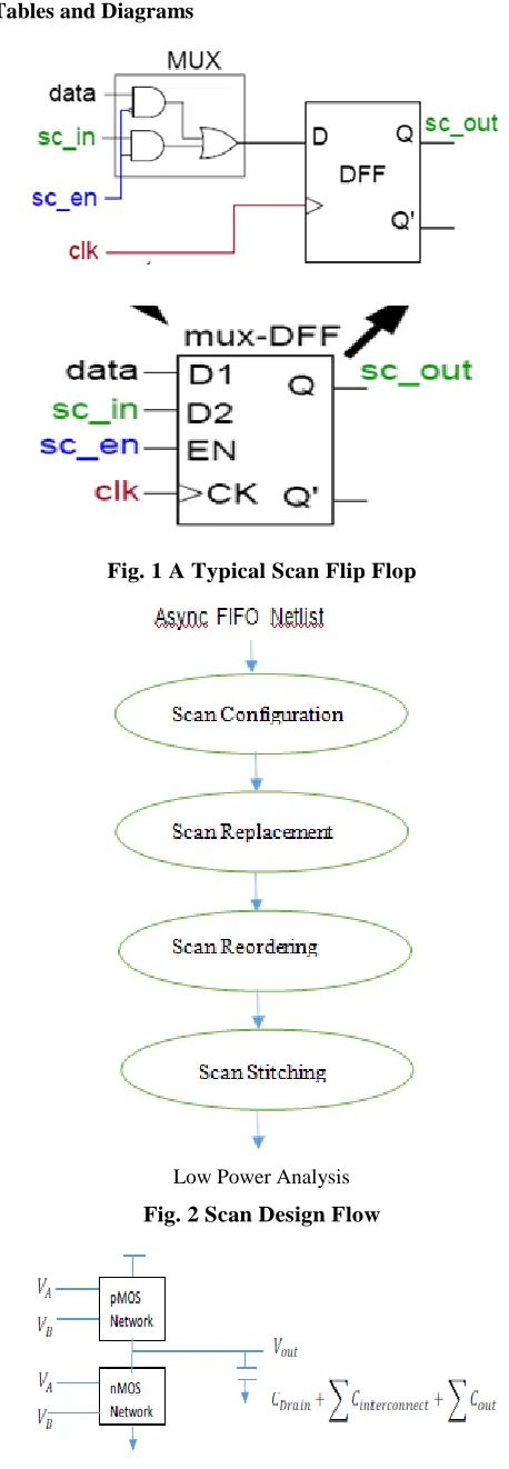
The technique applied in this paper is a novel technique by the authors who are doing research on Low Power Design Techniques on Design for Testability methodology. This technique is scan clock reduction technique which is reducing the scan clock frequency for testability purpose without affecting any functionality or performance of the chip. Reducing the scan clock does not affect the performance of the chip because; the scan clock is used only for testing the manufacturing defects and it does not affect the functionality of the design. In every Design for Test methodology, every functional flop is replaced by an equivalent scan flop which is controlled by a signal scan enable. When scan enable is set to logic ‘1’, then the test path is enabled and the functional path is disabled so that the functionality and the performance of the design is not affected.
Asynchronous FIFO Design
A typical asynchronous FIFO is used to synchronize data between two different clock domains. The read and write
Implementation of Asynchronous FIFO using
Low Power DFT
operations happen at different clocks viz. write happens in the write clock domain and read happens in the read clock domain. Both the clock domains and asynchronous to each other. The Asynchronous FIFO design used in this paper is architected using a novel implementation, where, a signal last operation is used to detect the fifo full and fifo empty flags. When the write pointer is equal to the read pointer and the last operation is a write, then the fifo full flag is asserted and when the write pointer is equal to the read pointer and the last operation is a read, the fifo empty flag is asserted. This is how the fifo full and fifo empty flags are generated in this novel architecture of asynchronous FIFO Design.
Scan Design Phase
Scan synthesis is the process of converting a testable design into a scan design without affecting the functionality of the original design. As shown in fig 2: the different steps involved in the Scan Design Flow are as follows:
(i) Scan Configuration
Number of scan chains used
Type of scan cells used to implement these scan chains
Types of storage elements to exclude from the process
Arranging the scan cells (ii) Scan Replacement
Replaces all original flip flops with their equivalent scan flip flops.
(iii)Scan Reordering
The process of reordering the scan chains based on the physical scan cell locations, in order to minimize the amount of interconnect wires used to implement the scan chains. (iv)Scan Stitching
Stitch all scan cells together to form scan chains. During the ATPG Simulations phase, the following steps take place: 11
a) Read Synthesis Net list from Design
b) Read ATPG Library Files, test procedure files and do files
c) Build ATPG Model d) ATPG DRC Checking e) Generate Fault List f) Generate Test Vectors
g) Validate Test Patterns Using Simulations
Low Power Specification Formats
The two common formats used in the Industry for Power savings are:
i. Unified Power Format(UPF) ii. Common Power Format(CPF)
While UPF Design flow is implemented with the help of Synopsys electronic design automation tools and tested on Synopsys generic 90nm and 32/28nm libraries, CPF Design flow was designed by Cadence Design Systems and then contributed to Si2. UPF has been driven mainly by Synopsys, Mentor Graphics and Magma. There is very subtle difference between the two flows. Most of the companies follow both the flows. Either of these flows are used to reduce power consumption at various levels of the ASIC Design Flow. [12]
II. LOW POWER DFT TECHNIQUES
Some of the commonly used low power techniques for
DFT used in the industry are:
a) Clock Gating Circuitry
It is a technique used for reduction of power consumption in power-on domain by blocking the clock dynamically before reaching a set of flip flops or latches. It is like switching off the clock when it is not being used functionally. Since continuous switching consumes lot of dynamic power, this technique helps to save power when clock is not being used. [13]
b) Power Domains
Separating the whole design into different power domains will ensure that each one of the block can powered down or powered up individually by controlling the power switches utilized for gating the power supply connection to every power domain block. [14]
c) Low Power Cell
While testing the design, the capacity of the State preservation registers to keep hold of their state needs to be verified when the power domain is powered off. Isolation cells are located at the limit of two power domains keeping in mind to isolate the power-on and power-off domains.
d) Multiple Supply Voltages
Based upon the operating conditions, different power domain blocks are subject to different supply voltages, and each power domain block is connected to other power domain block with the help of level shifters.
e) Power Aware DFT
Once the Scan synthesis starts, the functional flops are replaced by their scan equivalent flops. During the scan stitching process, the power aware DFT is applied by the respective power domain after the partitioning of scan chains under the condition that there are adequate scan I/O’s in every power domain and they can have their dedicated scan I/O’s, control signals and test clocks.
This guarantees that every power domain is having dedicated scan chains which are active in the power domain which in ON. [15][16]
f) Power Switches
In order to minimize the power dissipation, particularly leakage power dissipation caused by the shrinking power technologies, power switches are generally employed in modern low power design circuits. One or more power switches are equipped at different parts of the design to facilitate the functionality of power gating.
III. IMPLEMENTATION OF THE LOW POWER DFT TECHNIQUE
International Journal of Innovative Technology and Exploring Engineering (IJITEE) ISSN: 2278-3075, Volume-8 Issue-6S, April 2019
The input design is a PLL with multiple clocks. The gate level net list is taken as input for doing the DFT process and implementing the low power DFT technique of decreasing the SCAN Clock frequency and dividing it into multiple power domains. Here the emphasis is on reducing the dynamic power.
The general representation of CMOS logic gate for Switching Power Calculation is shown in fig3:
The average power consumption can be expressed as
The transition rate of the nodes can be slower than that of the clock rate. For better representation of this behavior, a node transition factor (∝') must be introduced
The generalized expression for the average power dissipation can be rewritten as
As we can see from Equation 4, Power is directly proportional to the clock frequency. Hence, reducing the clock frequency such that it falls between the specification ranges, the power can be reduced without affecting the timing violations there by.
IV. RESULTS
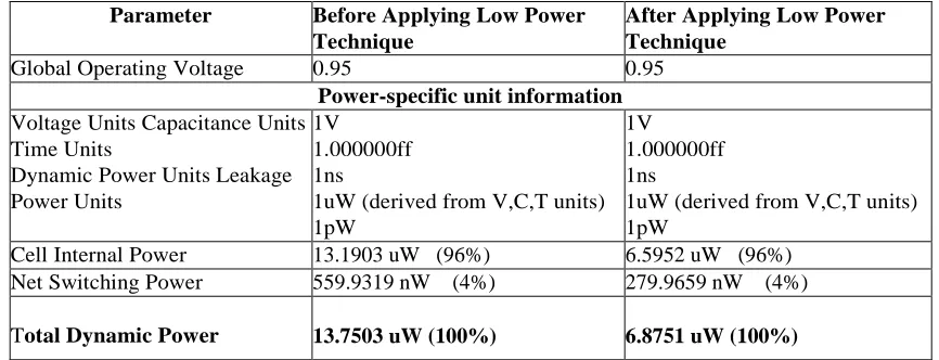
The results of this experiment at the Scan Synthesis level, after varying the scan clock frequency is tabulated in Table 1 As can be seen from the table.1 it is evident that the power has reduced by approximately 50%.
By reducing the scan clock frequency by half, the power also has reduced by 50% which is compliant to the equation 2. This is the reduction technique for dynamic power which is also the switching power in any SoC. Here, the reduction in the scan clock frequency does not affect the functionality of the design and neither the performance of the design, The scan enable of the scan flip flop ensures that only the test path of the chip is enabled and not the functional path. The functional path is disabled during the DFT phase.
From the fig 4, we can observe the decrease in power after applying the low power technique in Design for Test methodology as discussed in section3.
V.CONCLUSION
As, we can see from the above results, when the clock frequency is reduced from 50 MHz to 25 MHz, the power is also reduced by nearly 50%. What is important here, is that these results have been calibrated by ensuring that there are no setup or hold violations in the circuit after varying the clock frequency. The equation 3 clearly is henceforth proved that power is directly proportional to frequency. One of the next techniques which will be applied in the next version of the paper will be dividing the SCAN Clock for even and odd chains and thereby reducing the power consumption in the scan chain.
[image:3.595.309.538.52.713.2]Tables and Diagrams
Fig. 1 A Typical Scan Flip Flop
Low Power Analysis
Fig. 2 Scan Design Flow
Fig. 4 Graphical representation of power comparison for the Asynchronous FIFO Design
Table. 1 Comparison table showing the power values before and after applying Low power technique for Asynchronous FIFO
Parameter Before Applying Low Power Technique
After Applying Low Power Technique
Global Operating Voltage 0.95 0.95
Power-specific unit information Voltage Units Capacitance Units
Time Units
Dynamic Power Units Leakage Power Units
1V 1.000000ff 1ns
1uW (derived from V,C,T units) 1pW
1V 1.000000ff 1ns
1uW (derived from V,C,T units) 1pW
Cell Internal Power 13.1903 uW (96%) 6.5952 uW (96%)
Net Switching Power 559.9319 nW (4%) 279.9659 nW (4%)
Total Dynamic Power 13.7503 uW (100%) 6.8751 uW (100%)
REFERENCES
1. Design_for_testing ,https://en.wikipedia.org/wiki/ 2. low-power-design-for-testability,
https://www.design-reuse.com/articles/32262/low-power-design-for-testability.html
3. https://www.synopsys.com/content/dam/synopsys/implementation&sign off/white-papers/Testing-LP-PATest-WP.pdf
4. G. Rajesh Kumar, K. Babulu, A novel Architectre for Scan Cell in Low Power Test Circuit, [5] Procedia of Material Sciences, 10(2015), pp:403-408
5. Patrick Girard ,Survey of Low Power Testing of VLSI Circuits, IEEE Design and Test, 19(2002),pp:82-92.
6. PatrickGirard,LowPowerTestingofVLSICircuits:ProblemsandSoluti ons.pdf
7. Sandeep Bhatia, Low Power Compression Architecture, IEEE VLSI Test Symposium,10(2010).
8. AugusliKifli, Y.W. Chen, Y.W. Tsay, K.C. Wu, A Practical DFT Approach for Complex [10] Low Power Designs, Asian Test Symposium,2009
9. http://ieeexplore.ieee.org/document/5359399/ 10.
https://www.mentor.com/products/silicon- yield/resources/overview/using-tessent-low-power-test-to-manage-switching-activity-f1172890-a1af-40ca-a20a-406fd11c0907 11. https://www.hindawi.com/journals/vlsi/2015/264071/
12. http://www.sciencedirect.com/science/article/pii/S01679260163019 61
13. https://www.eetimes.com/document.asp?doc_id=1271843 14. http://citeseerx.ist.psu.edu/viewdoc/download?doi=10.1.1.121.8648
&rep=rep1&type=pdf
15. http://www.ee.ncu.edu.tw/~jfli/vlsi21/lecture/ch04.pdf 16. A.Nebhrajani, Asynchronous FIFO architectures,
http://vlsi_book/Asynch1.pd
17. AvinashYadlapati, Hari Kishore Kakarla, “An Advanced AXI Protocol Verification using Verilog HDL”, Wulfenia Journal, ISSN: 1561-882X, Volume 22, Number 4, pp. 307-314, April 2015.
18. P Ramakrishna, K. Hari Kishore, “Design of Low Power 10GS/s 6-Bit DAC using CMOS Technology “International Journal of Engineering and Technology(UAE), ISSN No: 2227-524X, Vol No: 7, Issue No: 1.5, Page No: 226-229, January 2018.
19. A Murali, K. Hari Kishore, “Efficient and High Speed Key Independent AES Based Authenticated Encryption Architecture using FPGAs “International Journal of Engineering and Technology(UAE), ISSN No: 2227-524X, Vol No: 7, Issue No: 1.5, Page No: 230-233, January 2018
20. K Bindu Bhargavi, K Hari Kishore “Low Power BIST on Memory Interface Logic”, International Journal of Applied Engineering Research, ISSN 0973-4562, Volume 10, Number 08 , pp. 21079-21090, May 2015.
21. K Hari Kishore, CVRN Aswin Kumar, T Vijay Srinivas, GV Govardhan, Ch Naga Pavan Kumar, R Venkatesh “Design and Analysis of High Efficient UART on Spartran-6 and Virtex-7 Devices”, International Journal of Applied Engineering Research, ISSN 0973-4562, Volume 10, Number 09 , pp. 23043-23052, June 2015.
22. Korraprolu Brahma Reddy, K Hari Kishore, “A Mixed Approach for Power Dissipation Reduction in Nanometer CMOS VLSI circuits”, International Journal of Applied Engineering Research, ISSN 0973-4562 Volume 9, Number 18 , pp. 5141-5148, July 2014.
23. Nidamanuri Sai Charan, Kakarla Hari Kishore "Reorganization of Delay Faults in Cluster Based FPGA Using BIST” Indian Journal of Science and Technology, ISSN No: 0974-6846, Vol No.9, Issue No.28, page: 1-7, July 2016.
0 5 10 15
Before Applying Low Power Technique (uW)
After Applying Low Power Technique (uW)
Async FIFO Power Comparison
[image:4.595.81.514.286.452.2]International Journal of Innovative Technology and Exploring Engineering (IJITEE) ISSN: 2278-3075, Volume-8 Issue-6S, April 2019
24. SravyaKante, Hari Kishore Kakarla, AvinashYadlapati,"Design and Verification of AMBA AHB-Lite protocol using Verilog HDL" International Journal of Engineering and Technology, E-ISSN No: 0975-4024, Vol No.8, Issue No.2, Page: 734-741, May 2016.
25. N Bala Dastagiri K Hari Kishore “A 14-bit 10kS/s Power Efficient 65nm SAR ADC for Cardiac Implantable Medical Devices” International Journal of Engineering and Technology (UAE), ISSN No: 2227-524X, Vol No: 7, Issue No: 2.8, Page No: 34-39, March 2018. 26. P. Sahithi K Hari Kishore, E Raghuveera, P. Gopi Krishna “DESIGN
OF VOLTAGE LEVEL SHIFTER FOR POWER-EFFICIENT APPLICATIONS USING 45nm TECHNOLOGY” International Journal of Engineering and Technology(UAE), ISSN No: 2227-524X, Vol No: 7, Issue No: 2.8, Page No: 103-108, March 2018.
27. Mahesh Mudavath and K Hari Kishore "Design of RF Front End CMOS Cascade CS Low Noise Amplifier on 65nm Technology Process” International Journal of Pure and Applied Mathematics, ISSN No: 1314-3395, Vol No: 115, Issue No: 7, Page No: 417-422, September 2017.
28. Bandlamoodi Sravani, K Hari Kishore, “An FPGA Implementation of Phase Locked Loop (PLL)”, International Journal of Applied Engineering Research, ISSN 0973-4562, Volume 10, Number 14 , pp. 34137-34139, August 2015.
29. Y Avinash, K Hari Kishore ‘’Designing Asynchronous FIFO for Low Power DFT Implementation’’ International Journal of Pure and Applied Mathematics, ISSN No: 1314-3395, Vol No: 115, Issue No: 8, Page No: 561-566, September 2017.
30. AvinashYadlapati, Kakarla Hari Kishore,”Constrained Level Validation of Serial Peripheral Interface Protocol”, Proceedings of the First International Conference on Smart Innovation, Systems and Technologies 77, ISSN No: 2190-3018, ISBN: 978-981-10-5544-7, Chapter No: 77, pp. 743-753, 25th December 2017.
31. Meka Bharadwaj, Hari Kishore "Enhanced Launch-Off-Capture Testing Using BIST Designs” Journal of Engineering and Applied Sciences, ISSN No: 1816-949X, Vol No.12, Issue No.3, page: 636-643, April 2017.
32. P Bala Gopal, K Hari Kishore, R.R Kalyan Venkatesh, P Harinath Mandalapu “An FPGA Implementation of On Chip UART Testing with BIST Techniques”, International Journal of Applied Engineering Research, ISSN 0973-4562, Volume 10, Number 14 , pp. 34047-34051, August 2015.
33. A Murali, K Hari Kishore, D Venkat Reddy "Integrating FPGAs with Trigger Circuitry Core System Insertions for Observability in Debugging Process” Journal of Engineering and Applied Sciences, ISSN No: 1816-949X, Vol No.11, Issue No.12, page: 2643-2650, December 2016.
34. Mahesh Mudavath, K Hari Kishore, D Venkat Reddy "Design of CMOS RF Front-End of Low Noise Amplifier for LTE System Applications Integrating FPGAs” Asian Journal of Information Technology, ISSN No: 1682-3915, Vol No.15, Issue No.20, page: 4040-4047, December 2016.
35. N Bala Dastagiri, Kakarla Hari Kishore "Reduction of Kickback Noise in Latched Comparators for Cardiac IMDs” Indian Journal of Science and Technology, ISSN No: 0974-6846, Vol No.9, Issue No.43, Page: 1-6, November 2016.
36. K Hari Kishore, K DurgaKoteswara Rao, G Manvith, K Biswanth, P Alekhya “Area, Power and Delay Efficient 2-bit Magnitude Comparator using Modified GDI Technique in Tanner 180nm Technology “International Journal of Engineering and Technology(UAE), ISSN No: 2227-524X, Vol No: 7, Issue No: 2.8, Page No: 222-226, March 2018.
37. P Kiran Kumar, P Prasad Rao, Kakarla Hari Kishore, “Optimal Design of Reversible Parity Preserving New Full Adder / Full Subtractor”, Proceedings of 2017 11th International Conference on Intelligent Systems and Control, ISCO 2017, pp. 368-373, , 25th and 26th February 2017.
38. A Murali, K Hari Kishore, C P Rama Krishna, S Kumar, A Trinadha Rao “Integrating the Reconfigurable Devices using Slow-changing Key Technique to achieve High Performance ”Proceedings- 7th IEEE International Advance Computing Conference, IACC 2017, 7976849 ISSN: 2473-3571, pp.530-534, July 2017.
39. Nadhindla Bala Dastagiri, Kakarla Hari Kishore, Vinit Kumar Gunjan and Shaik Fahimuddin, “Design of a Low-Power Low-Kickback-Noise Latched Dynamic Comparator for Cardiac Implantable Medical Device Applications”, Proceedings of 2nd International Conference on Micro-Electronics, Electromagnetic and Telecommunications, Lecture Notes in Electrical Engineering, ISSN No: 1876-1100, E-ISSN: 1876-1119,
pp. 637-645, 29th March 2017.
40. G. Vijaya Padma, K. Hari Kishore and S. Jaya Sindura, “Controlling the Traffic Interactions with High Mobility and Constant Network Connectivity by Vanets”, Proceedings of 2nd International Conference on Micro-Electronics, Electromagnetic and Telecommunications, Lecture Notes in Electrical Engineering (Publisher: Springer Nature Singapore Pte Ltd), ISSN No: 1876-1100, E-ISSN: 1876-1119, pp. 593-601, 29th March 2017.
41. A Murali, K Hari Kishore, L Srikanth, A Trinadha Rao and V Suresh, “Implementation of Reconfigurable Circuit with Watch-Points in the Hardware”, Proceedings of 2nd International Conference on Micro-Electronics, Electromagnetic and Telecommunications, Lecture Notes in Electrical Engineering, ISSN No: 1876-1100 , E-ISSN: 1876-1119, pp. 657-664, 29th March 2017.
42. K.Sarath Chandra, K Hari Kishore “Physical Design Implementation of High Performance CMOS Dynamic Latch Comparator” Journal of Advanced Research in Dynamical and Control Systems, ISSN No: 1943-023X, Vol No: 10, Special Issue No: 9, Page No: 323-332, June 2018.
43. P Ramakrishna, K Hari Kishore “DESIGN OF AN ULTRA LOW POWER CMOSCOMPARATOR FOR DATA CONVERTERS” Journal of Advanced Research in Dynamical and Control Systems, ISSN No: 1943-023X, Vol No: 10, Special Issue No: 7, Page No: 1347-1352, June 2018. 44. Avinash Yadlapati, K Hari Kishore “System Level Verification of
Advanced Extensible Interface Protocol Using Verilog HDL” Journal of Advanced Research in Dynamical and Control Systems, ISSN No: 1943-023X, Vol No: 10, Special Issue No: 7, Page No: 1359-1365, June 2018.
45. Meka Bharadwaj, Hari Kishore "Enhanced Launch-Off-Capture
Testing Using BIST Designs” Journal of Engineering and Applied Sciences, ISSN No: 1816-949X, Vol No.12, Issue No.3, page: 636-643, April 2017.
46. Dr. Seetaiah Kilaru, Hari Kishore K, Sravani T, Anvesh Chowdary L, Balaji T “Review and Analysis of Promising Technologies with Respect to fifth Generation Networks”, 2014 First International Conference on Networks and Soft Computing,ISSN:978-1-4799-3486-7/14,pp.248-251,August 2014.