Sparse Matrix-Vector Products in
Statistical Machine Learning
Applications
Ahmed H. El Zein
April 2009
? p \ k^>3
) Jiill lii Ji*l jtjjt
The work in this thesis is my own except where otherwise stated.
Ahmed H. El Zein
A cknow ledgem ents
I am indebted to many people without whom I would have not completed this project. At the top of the list is my supervisor, Alistair Rendell. I would not have been able to achieve anything without his mentoring, support and obvious care for my well-being. For all this, I am deeply grateful.
I would like to thank Alex Smola for his help and support. My thanks also go out to Muhammad Atif and Danny Robson for making coffee breaks fun, to Jin Wong for putting up with me in a single office for two years, to Warren Armstrong and Josh Milthorpe for proof reading my thesis and to Peter Strazdins, Eric McCreath, Pete Janes, Jie Cai, Arrin Daley and Joseph Anthony who make up the rest of the HPC research group for being my friends.
To Bob Edwards, Deanne Drummond, Suzanne Van Haeften and Julie Arnold, thank you for making my journey as smooth as possible.
I would also like to thank my wife, Eman who put up with long nights at Uni, my daughter, Mariam who went to sleep many nights calling out “Daddy kiss!” without getting her good-night kiss, my sister who kept my wife company while I was writing this, my mother and father who made me what I am, and the rest of my family, thousands of miles away whose support I depend on.
Thank you all.
Graphics Processing Units (GPUs) offer orders of magnitude more floating-point performance than conventional processors. Traditionally, however, accessing this performance for general purpose programming has required the user to cast their problem into a graphical framework of nodes and vertices. In 2007 this situation changed dramatically when NVIDIA released its CUDA programming model for GPUs.
The objective of this thesis is to assess the viability of using an NVIDIA GeForce 8800 GTX GPU and the CUDA programming model for statistical ma-chine learning (SML) applications.
At the heart of the SML method is the iterative solution of a set of equations. Each iteration involves two matrix-vector products, where the matrix is generally sparse and does not change between iterations. Key issues considered in this work are what fraction of the SML application should be migrated to the GPU, the cost of moving data to and from the GPU, the efficient implementation of Sparse Matrix-Vector products (SpMV) on the GPU, and the relative merits of using sparse versus dense matrix routines.
In implementing the SpMV routine on the GPU a range of different CUDA options were considered, including the type of memory used to store different data quantities, the use of float, float2 and float4 data types, the number of threads per block, the use of coalesced memory reads etc. Following a preliminary performance characterisation of the 8800 GTX, 335 different SpMV implementa-tions were constructed and their performance tested using 735 matrices from the Florida sparse matrix collection. From this a small number of best performing implementations were identified and an attempt made to create a blackbox im-plementation that would correctly select the optimal imim-plementation for a given sparse matrix type.
Contents
Acknowledgements vii
Abstract ix
1 Introduction 1
2 Background 5
2.1 Programming GPUs ... 5
2.1.1 Shader Languages... 6
2.1.2 Languages for General Purpose C om puting... 7
2.2 Target H a rd w a re ... 8
2.2.1 The CUDA Programming Model ... 9
2.2.2 GeForce 8800 GTX Memory H ierarch y... 10
2.2.3 The CUDA Execution Model ... 13
2.3 Statistical Machine Learning... 13
2.4 Sparse M atrices... 14
2.5 Sparse Matrices on GPUs: Previous W o r k ... 16
3 Dense M atrix-Vector Performance 19 3.1 Hardware and Software S e tu p ... 20
3.2 Bandwidth between the Host and G P U ... 22
3.3 Dense Matrix-Vector Perform ance... 23
3.3.1 Effect of Size on Dense Matrix-Vector Performance . . . . 24
3.3.2 Effect of Shape on Perform ance... 31
3.3.3 Conclusion... 34
4 SpM V Construction and Evaluation 35 4.1 Memory Bandwidth Analysis ... 37
4.1.1 Coalesced Memory Benchmark R e s u lts ... 39
CONTENTS
xii
4.1.2 Sequential Memory Benchmark R esu lts... 41
4.1.3 Coalesced vs Sequential Memory for SpM V ... 42
4.2 SpMV Implementations ... 42
4.3 Performance Evaluation M ethodology... 45
4.3.1 Evaluation P la tf o rm ... 45
4.3.2 Test M atrice s... 45
4.3.3 Performance Measurements ... 48
4.4 SpMV Implementation A ssessm ent... 48
4.4.1 Evaluating vec Storage O p tio n s... 49
4.4.2 Evaluating ptr Storage O p tio n s... 53
4.4.3 Coalesced v Sequential SpMV Im plem entations... 56
4.4.4 Multiple Row Implementations ... 59
4.4.5 Evaluation of Selected Implementations... 61
4.5 Mapping Matrices to their Optimal Im plem entation... 65
4.5.1 Selecting the Number of Threads per Block ... 70
4.6 CPU v blackbox Perform ance... 71
4.7 Recent Related W o rk ... 73
4.8 Summary and Conclusion ... 76
4.9 Results on a GTX 295 G P U ... 77
5 SML Application 79 5.1 Conclusion... 85
6 Conclusions and Future Work 87
A M emory Bandwidth Benchmarks 91
Chapter 1
Introduction
For the past few years, the demand for more realistic games in an ever growing market has led GPU manufacturers to produce high end graphics cards that are able to render complex scenes at very fast frame rates. As graphics problems are highly parallel in nature, GPUs have been designed as massively parallel archi-tectures. Furthermore, to deal with the developments in graphics programming and the increasingly complex processing, GPUs have gradually made a transition from fixed-function pipeline devices that are only able to perform fixed opera-tions, to general purpose processors with some special graphics oriented units. The large commodity GPU market and ruthless competition have realised rel-atively low cost devices with very high Floating-Point Operations per Second (FLOP/s) ratings.
GPUs use Single Instruction Multiple Data (SIMD) architectures to minimise control logic and power requirements, providing a greater number of FLOP/s per watt than CPUs. CPUs attempt to mask memory latencies with large amounts of cache comprising a significant portion of the CPU die space [25, 30]. In contrast, GPUs have minimal amounts of cache, relying on the ability to execute thousands of threads in parallel, masking memory latencies by switching between the large number of threads [42]. The die space saved by these methods can be invested in Arithmetic Logic Units (ALUs). The overall result is a less versatile general purpose processor that has a much lower cost per FLOP (both in terms of price and power requirements) and a much higher peak FLOP/s rating. For the past few years, the gap between CPUs and GPUs has been growing in this regard [46].
Throughout the evolution of GPUs, the difficulty of programming these de-vices has deterred wide adoption by the scientific community. Until recently, GPUs only supported domain specific, graphics oriented languages. Describing
2
CHAPTER 1. INTRODUCTION
scientific problems in terms of graphics primitives is a daunting task that requires a strong understanding of graphics programming. Higher level but still domain specific languages were designed to make programming GPUs easier [35, 27, 47]. Yet, while General Purpose computation on GPUs (GPGPU) became easier, the hardware itself hampered GPGPU by not supporting many of the features used in general purpose programming such as scatter operations, thread synchronisation and shared memory [13].
ATI and NVIDIA (two of the largest GPU manufacturers) eventually released GPUs with completely programmable processors [45]. The new unified architec-tures also provided the missing hardware feaarchitec-tures (scatter operations, shared memory, synchronisation) that were required for GPGPU. To facilitate GPGPU programming for these GPUs, ATI AND NVIDIA released programming toolkits for them [42, 4]. However while ATI released an assembly like language, NVIDIA released a C /C + + syntax compatible language named CUDA, which allowed the programmer to mix CPU and GPU code in the same module. NVIDIA and to a lesser extent ATI, finally presented the scientific community with easy to program, massively parallel multi-threaded devices with many of the hardware capabilities needed to efficiently execute scientific applications.
In 2007, GPU hardware lacked double-precision floating-point support which held back its adoption by many within the scientific community [23]. Current GPUs from both manufacturers offer double-precision but with lower FLOP/s the for single precision. ECC memory has not been announced for any upcoming products by either of the manufacturers.
For many scientific applications, the lack of ECC memory and double-precision are not important. The application can be robust enough to deal with bit flips and not all applications require double-precision. For many other applications, numerical methods can be used to produce high precision results [44] and still perform better on the GPU than the CPU [23].
Internet searching is a high profile SML application. Companies like Google, Yahoo and Microsoft all spend enormous amounts of money on server hardware and power costs of running the servers. Solutions that lower the cost of com-putations either by increasing the throughput of systems with the same power requirements or decreasing the power requirements of a system that maintains the same throughput are of huge benefit in terms of running costs. GPUs offer potential solutions in this area.
The Bundle Methods for Regularised Risk Minimisation (BMRM) application is an open source, modular and scalable convex solver for many machine learning problems [54]. A portion of these problems are not affected by the use of single precision. This SML application’s computation is dominated by matrix-vector products which depending on the nature of the datasets can be either dense and sparse. Dense matrix-vector products are easily parallelised and have been shown to perform well on GPUs [21, 33, 31]. Sparse matrix-vector products on GPUs have not been as successful as their dense counterparts, but the new unified ar-chitectures are potentially flexible enough to provide performance improvements for Sparse Matrix-Vector products (SpMV) on the GPU. SpMV on GPUs will be discussed in more detail in the next chapter.
CUDA provides a Basic Linear Algebra Subprograms (BLAS) library (CUBLAS [40]) that is utilised to evaluate matrix-vector products on the GPU. NVIDIA did not provide SpMV routines at the start of this work and so SpMV routines were developed and evaluated on the GPU as part of this work. This work is based on the GeForce 8800 GTX as it was the best performing product from NVIDIA at the start of this work.
Chapter 2
Background
This section presents background information on General-Purpose computation on GPUs (GPGPU), details of the GeForce 8800 GTX GPU and the CUDA programming environment used in this work. This section also discusses sparse matrices and provides more details on the SML algorithm used in the BMRM application.
2.1 P rogram m ing G P U s
GPUs were first introduced as non-programmable, fixed-function pipelines with specific functions. The GPU starts with a scene defined by a list of coordinates call vertices. Each vertex undergoes a series of transformations with the end being a “pixel” that will then be displayed on the screen. Vertices that will not end up on the screen (they could be hidden by other vertices for example) are ignored. Each pixel is then given a color based on attributes such as texture and lighting and the the end result is a frame to be displayed on the screen.
Later, products were released [46] that contained embedded programmable components. The series of transformations applied to the vertices as well as the pixel colouring could be programmed in the form an assembly language. These programs are referred to as vertex shaders and pixel or fragment shaders.
As the instructions sets of these embedded components grew, so did the com-plexity and length of the shader programs. It soon became unrealistic to write shaders in the assembly level languages provided by the vendors. This gave rise to higher level languages that varied in their specification yet all attempted to make shader programming easier [45].
Higher level languages made GPGPU a lot easier, but they were still
signed from a graphics perspective so were not easily accessible to scientists with a non-graphics background. Indeed GPGPU with these languages required a considerable amount of graphics knowledge in order to map a general problem into a graphics problem solvable with graphics APIs. To simplify the process of writing general purpose code for GPUs, GPGPU languages came into existence. The following subsections consider some of the languages that are available for GPGPU.
A much wider survey of available options for programming GPUs has been published by Owens et al. [46] in 2007. This survey summarises and analyses the latest research in GPGPU.
2.1.1 Shader Languages
This class of languages facilitates the writing of shaders but with added portability and programmer productivity. A separate shader program must be written for each of the vertex and fragment processors. These languages also differ in many aspects that will be illustrated in the relevant sections.
Cg
Cg (or C for graphics) [35] differs from the other languages in this section in that it has a clear separation between code meant to run on the CPU and code intended for the GPU. Cg attempts to find a balance between providing the whole feature set of C and providing a maximum shader feature set. For example it omits many high level shader-specific facilities yet provides the same operators as C (but ones that accept and return vectors as well as scalars). Cg is compiled into an assembly level language for either OpenGL [53] or Direct3D [11].
O penG L Shading Language
2.1. PROGRAMMING GPUS
7The Direct 3D High-Level Shading Language
The Direct 3D High-Level Shading Language (HLSL) [47] was developed in close partnership with NVIDIA and is similar in many aspects to Cg. As part of Direct3DX, it only compiles to Direct3D and is only supported on Microsoft operating systems [47].
2.1.2 Languages for General Purpose C om puting
These languages differ from the previous languages in that they are more suited to general purpose computing. However they offer the programmer less control over the graphics pipeline.
Shader M etaprogramming Language
Sh is both a shading language and a runtime API to use the Sh shaders [37]. It is embedded in C + + as a domain specific language and defines special tuple and matrix types that are used extensively in shader code. Sh can be used to write vertex or fragment shaders for a GPU in C /C + + . The code is then compiled at runtime to the target device [37]. Sh can also treat shaders as first class objects and by combining connection and combination features in Sh allow the creating of complex stream programs for GPGPU computing [36]. In Sh there is no clear distinction between GPU and CPU code, nor is there any explicit mechanism to move data to and from the GPU memory.
Brook and BrookG PU
Brook is an extension of standard ANSI C and is designed to incorporate the ideas of data parallel computing and arithmetic intensity into a familiar and efficient language. BrookGPU, a GPU targeted version of Brook was developed by Buck et al. [15] based on the idea that a GPU can be viewed as a stream processor.
that run in turn on the GPU to accommodate the extra outputs needed. This virtualisation can also be used to provide complex data types not supported by the hardware [15].
C for CUDA
CUD A is an architecture and programming model for parallel computing devel-oped by NVIDIA. NVIDIA provides a C like API called C for CUDA. The CUDA architecture, programming model and development environment are expanded upon in section 2.2.
2.2 Target H ardw are, Language, E xecution and
Program m ing M odel
The GeForce 8 Series GPUs were the first NVIDIA GPUs to be based on the new “unified architecture”. Figure 2.1 illustrates the architecture of the GeForce 8800 GTX used in this work. At the heart of the device lies the Streaming Processor Ar-ray (SPA) consisting of eight Texture Processor Cluster (TPC) units. Each TPC contains two Streaming Multiprocessor (SM) units and a texture unit. The SM in turn consists of eight Stream Processors (SP), a special function unit, a 8192 wide register file and 16KB of shared memory. When running CUDA applications each SP (clocked at a default of 1.35 GHz) is able to issue one multiply-add (MAD) in-struction per cycle. This gives each SM a peak performance of 1.359 x 8 x 2-f230 = 20.1 GFLOP/s, and the GeForce 8800 GTX with 16 SMs an aggregate perfor-mance of 321.6 GFLOP/s. The GeForce 8800 GTX has 768 MB of global, frame buffer memory that can be read from or written to by the host CPU as well as the GPU. The 768MB of GDDR3 memory is clocked at 900MHz and is accessed via a 384-bit (48 byte) wide interface in 128-bit wide words. This gives a theoretical
peak bandwidth of (48 bytes x 900 x 106 M H z x 2 (DDR)) -y 230 = 80 GB/s.
2.2. TARGET HARDWARE 9
/ i l
Streoming Processor Array
Y
y
\(
‘ 1 1 —F—T—F—F- F ^
X i ^ I
Memory
Texture Processor C tust er
/
Streaming Multiprocessor Instruction LI Data LI
SM SM
Texture Unit
Instruction Fetctr/Dlspalch
ShoreO Memory
Streaming Processor \ j fL ADO, 5UB. MUL MAD. etcx [
Super Function Unit !_ . i SIN, PSORT. EXP. e tc j T-N
SP SFU
C D
[_ SP j
C
&J
SFUL 31 j
\
Figure 2.1: GeForce 8800 GTX architecture
Transform (FFT) implementations [40, 41] . The programming model, memory hierarchy and execution model defined by CUBA are expanded upon in the next sections.
2.2.1 The C U D A Program m ing M odel
Writing applications for CUDA enabled GPUs involves copying data from the host to the GPU memory, invoking the GPU code (in the form of one or more kernels) and copying the results of the computation back to the host. CUDA provides methods to allocate memory on the GPU as well as methods to copy data between GPU memory and host memory. CUDA also provides functions to allocate page-locked memory. Bandwidth to and from page-locked memory is faster, as DMA transfers must be done from page-locked memory and having the data in page-locked memory saves the driver from having to copy it to page-locked memory before initiating the DMA transfer.
blocks of between 1 and 512 threads. The GeForce 8800 GTX can accommodate up to 64K x 64K blocks in what CUDA labels a grid.
Threads are automatically assigned an index so that different threads can fetch data from different memory locations. Each thread is then able to retrieve the dimensions of the grid and block as well as its thread index within its block and its block index within the grid. As an aid to the programmer, CUDA offers 1, 2 or 3 dimensional indexing of the blocks if it would better suit the data. Only 1 or 2 dimensional indexing of the grid is supported.
Listing 2.1: Example kernel and host invocation methods with use of 2D indexing
_ _ g l o b a l __v o i d m a t Add ( f l o a t A [ N ] [ N ] , f l o a t B [ N ] [ N ] , f l o a t C [ N ] [ N ] )
{
i n t i = b l o c k l d x . x * b l o c k D i m . x + t h r e a d l d x . x ; i n t j = b l o c k l d x . y * b l o c k D i m . y + t h r e a d l d x . y ; i f ( i < N && j < N)
C [ i ] [ j ] = A [ i ] [ j ] + B [ i ] [ j ] ;
}
i n t m a i n ( )
{
/ * s e t t h e b l o c k s t o c o n t a i n 1 6 x16 t h r e a d s * / d i m 3 d i m B l o c k ( 1 6 , 1 6 ) ;
/ * t o t a l n u m b e r of b l o c k s d e p e n d s N * /
d i m 3 d i m G r i d ( ( N + d i m B l o c k . x — 1) / d i m B l o c k . x , (N + d i m B l o c k . y — 1) / d i m B l o c k . y ) ; / * K e r n e l i n v o c a t i o n » /
m a t A d d « < d i m G r i d , d i m B l o c k > » ( A , B, C ) ;
}____________
Listing 2.1 shows an example of a kernel using 2 dimensional indexing along with the code to invoke the kernel. Each block is executed on a single Streaming Multiprocessor (SM). Within the SM each thread executes on an SP. The large register file allows the SM to create more threads than available SPs. The number of threads that can be resident on the SM depends on the threads resource usage in terms of registers and shared memory. In fact an SM can accommodate multiple blocks if there exists enough resources for all the threads in the multiple blocks.
2.2.2 GeForce 8800 G TX M em ory Hierarchy
The GeForce 8800 GTX offers many different memory types, each with its ad-vantages and disadad-vantages. These memories are summarised in table 2.1.
on-2.2.
TARGET HARDWARE
11Table 2.1: Different Memory types available on the GeForce 8800 GTX GPU.
M em ory L ocation C ached H ost A ccess G P U A ccess Scope Lifetim e R egister O n-chip N /A N /A R /W O ne th re a d T h read
Local Off-chip No N /A R /W O ne th re a d T h read S hared O n-chip N /A N /A R /W All th re a d s in a block Block G lobal Off-chip No R /W R /W A ll th re a d s + h ost A pplication C o n sta n t O ff-chip Yes R /W R A ll th re a d s + h ost A pplication T ex tu re Off-chip Yes R /W R A ll th re a d s + h o st A pplication
chip shared memory divided into 16 banks such that successive 32-bit words are assigned to successive banks. Bank conflicts will incur performance hits. In the absence of conflicts shared memory reads are as fast as register reads [42]. Registers and local and shared memory are accessible from the GPU only.
Global memory is the main memory type of the GPU. It is the largest memory space and provides read and write access from both the host via DMA and the SMs. Global memory is not cached, relying instead on the thousands of threads running on the GPU to mask latency. Global memory has a latency of 400 - 600 cycles while a floating-point arithmetic instruction (ADD, MUL, SUB) has an issue latency of 4 cycles and a throughput of 8 operations per cycle [42]. The CUDA programming guide [39] states that in order to achieve optimal memory bandwidth, memory reads must be coalesced. This occurs when all 16 threads read from aligned, consecutive, memory addresses, and the hardware is able to transform the individual memory accesses into a number of 64-byte memory trans-actions. Coalesced 32-bit reads result in one 64-byte transaction, coalesced 64-bit reads result in a single 128-byte transaction and coalesced 128-bit reads result in two 128-byte transactions. Non-coalesced 32-bit reads are an order of magnitude slower than coalesced 32-bit reads. The coalescing rules described here are for the 8800 GTX GPU architecture. Latest generation GPUs have different (less strin-gent) rules. More information can be found in the CUDA programming manual, which has an extensive section on memory coalescing [42].
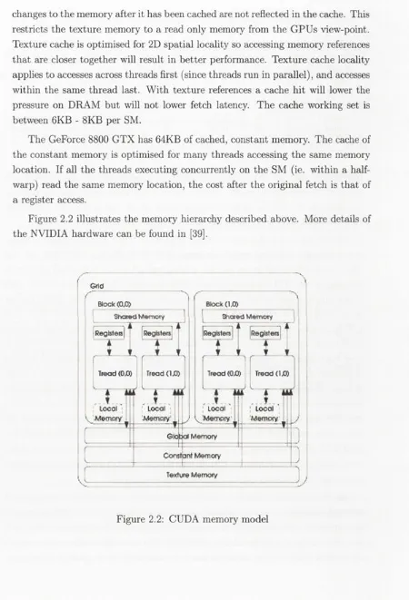
changes to the memory after it has been cached are not reflected in the cache. This restricts the texture memory to a read only memory from the GPUs view-point. Texture cache is optimised for 2D spatial locality so accessing memory references that are closer together will result in better performance. Texture cache locality applies to accesses across threads first (since threads run in parallel), and accesses within the same thread last. With texture references a cache hit will lower the pressure on DRAM but will not lower fetch latency. The cache working set is between 6KB - 8KB per SM.
The GeForce 8800 GTX has 64KB of cached, constant memory. The cache of the constant memory is optimised for many threads accessing the same memory location. If all the threads executing concurrently on the SM (ie. within a half-warp) read the same memory location, the cost after the original fetch is that of a register access.
Figure 2.2 illustrates the memory hierarchy described above. More details of the NVIDIA hardware can be found in [39].
Tread (0,0)
Shared Memory
Local ; lo ca l
Memory Block (0.0)
Constant Memory
[image:19.536.54.504.88.749.2]2.3. STATISTICAL MACHINE LEARNING 13
2.2.3 T h e C U D A E xecution M odel
When a kernel is launched on the device, the number of threads, blocks and grids are all specified at launch time. These values may be calculated based on the problem size, passed as parameters at run time or set as constant values. The thread scheduler will schedule blocks to available SMs. Each SM may be allocated multiple blocks depending on the resource usage of the block. As previously indicated, SMs can accommodate more threads than SPs. The SM will then execute all the threads in batches of 32 threads. These 32 threads are called a warp. Each warp is free to diverge from the others with no penalty. The warp is actually executed in two sets of 16 threads each. The SM will continue to execute all threads until they have all terminated at which time any remaining blocks can be scheduled to it. There are no guarantees on the order in which threads are executed or which blocks are scheduled before others. The CUDA programming guide recommends launching a large number of blocks on the device to ensure that memory latencies can be masked.
Threads in the same block can synchronise or shared data via the on-chip shared memory. However, this is not possible between threads of different blocks as only threads within the same block can be guaranteed to be resident on the SM at the same time.
2.3 S tatistical M achine Learning
One of the key objectives in Machine Learning (ML) is classification: given some
patterns such as pictures of apples and oranges, and corresponding labels
Ui, such as the information whether is an apple or an orange, to find some
function / which allows us to estimate y from x automatically. Statistical Machine
learning (SML) attempts to solve such problems with statistical methods. In this quest, convex optimisation 1 is a key enabling technology for many problems. For instance, Teo et al. [54] proposed a scalable convex solver for such problems. It is an iterative algorithm that involves guessing a solution vector te, using this to
evaluate a loss function l(x,y, w) (that calculates a penalty based on the amount
of error in the solution) and its derivative g = dwl(x,y,w), and then updating
w accordingly. This process is repeated until a desired level of convergence is
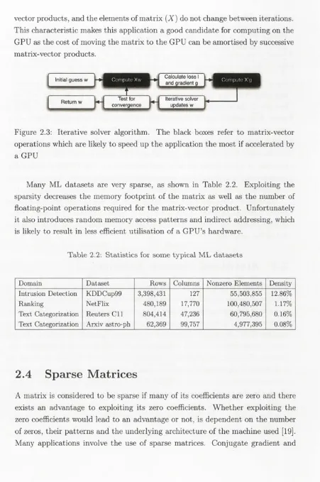
vector products, and the elements of matrix (X) do not change between iterations.
This characteristic makes this application a good candidate for computing on the
GPU as the cost of moving the matrix to the GPU can be amortised by successive
matrix-vector products.
Initial guess w
Return w convergence convergenceTest for Test for 1 Iterative solver U ___________|Iterative solverupdates wupdates w
Figure 2.3: Iterative solver algorithm. The black boxes refer to matrix-vector
operations which are likely to speed up the application the most if accelerated by
a GPU
Many ML datasets are very sparse, as shown in Table 2.2. Exploiting the
sparsity decreases the memory footprint of the matrix as well as the number of
floating-point operations required for the matrix-vector product. Unfortunately
it also introduces random memory access patterns and indirect addressing, which
is likely to result in less efficient utilisation of a GPU’s hardware.
Table 2.2: Statistics for some typical ML datasets
Dom ain D ataset Rows Colum ns Nonzero E lem ents Density Intrusion D etection K D D C up99 3,398,431 127 55,503,855 12.86% Ranking N etFlix 480,189 17,770 100,480,507 1.17% Text C ategorization R euters C ll 804,414 47,236 60,795,680 0.16% Text C ategorization A rxiv astro-ph 62,369 99,757 4,977,395 0.08%
2.4 Sparse M atrices
[image:21.536.47.498.78.757.2]2.4. SPARSE MATRICES
15multigrid solvers are often based on sparse matrix-vector products when used in fields such as computational fluid dynamics and mechanical engineering. Sparse matrices are also used in graph theory.
The exploitation of sparsity is achieved by discarding zero elements from the sparse matrix. By doing so the memory requirements and number of arithmetic operations needed for the matrix-vector product are greatly reduced. However, indirect random memory references are introduced as the index of each element must be explicitly stored in the sparse data structure and the memory reads from the vector will no longer be consecutive. Many different formats for storing these matrices have been designed to take advantage of the structure of the sparse matrix or the specificity of the problem from which they arise [50].
The Compressed Sparse Row (CSR) format is the most widely used of these formats [50, 10, 19]. The CSR format (also named Compressed Row Storage) stores non-zero elements in a dense vector val. For each value in val, its column index from the original matrix is stored in a dense vector of the same size ind at the same offset. A third array (ptr) carries the offset of the first element in every row. This is illustrated by figure 2.4. A Sparse Matrix-Vector products (SpMV) with a matrix in the CSR format is straightforward as shown by figure. 2.5.
• •
•
▼ T
val
•
1
*
!
1
• • ind 0 2 4 0 2 0 3 1
• •
ptr 0 2 3 5 | 7
Figure 2.4: CSR format
fo r each row i do
fo r l= p tr [i] to p t r [ i + l ] - l do
r e s f i] = res [i] + val [1] * v e c fin d fl]]
Figure 2.5: pseudo-code for Sparse Matrix-Vector product (SpMV).
a broad range of multicore architectures including a dual core AMD Opteron 2214, a quad core Intel Clovertown processor as well as a dual socket STI Cell Blade system and the 8 core Sun Niagara2 processor. The work evaluated a range of optimisations for each of the architectures and analysed the performance bottlenecks for all the architectures showing that the memory bandwidth is the common limiting factor in SpMV performance. Only 14 datasets were evaluated and results showed a median performance of 2 GFLOP/s for both the AMD and Intel CPUs, a median performance of 3 GFLOP/s for the Niagara2 processor and 6 GFLOP/s for the Cell Blade system.
2.5 Sparse M atrices on G PU s: P revious W ork
SpMV has not been a popular candidate for implementation on GPUs. This is due to the irregular nature of the problem, characterised by indirect addressing (array 1 [array2[index]]) [56]. Two GPU implementations of SpMV were published at SIGGRAPH’03. Bolz et al. [13] defined sparse matrices in the Modified Sparse Row (MSR) format and were able to perform 120 SpMV operations per sec-ond with a matrix containing 37k nonzero elements on a 500MHz GeForce FX GPU. That is equal to roughly 9 MFLOP/s. The second implementation was by Krüger et al. [31] targeting banded matrices and achieving a performance of about 110 M FLOP/s on an ATI Radeon 9800 GPU. In 2005 Ujaldon et al. [56] published SpMV results on a GeForce 6800. They achieved 222 MFLOP/s with the BCSSTK30 matrix (1036208 nonzero elements, stored in CSR format) from the Harwell-Boeing collection [20]. The Harwell-Boeing Sparse Matrix Collection is a set of standard test matrices arising from problems in linear systems, least squares, and eigenvalue calculations from a wide variety of scientific and engi-neering disciplines. The majority of the matrices are less than 1000 x 1000 and the collection contains 292 matrices.
More recently in Graphics Hardware 2007, Sengupta et al. [52] published SpMV results based on an efficient segmented scan using CUDA. This work is most relevant to the present work as the authors used the same hardware and programming language. Sengupta et al. [52] reported SpMV performance of 215 MFLOP/s for a 294,267 nonzero element matrix. These results are comparable to those published by Ujaldon et al. [56] almost 2 years prior. They are also just below that of CPU implementations at the time [52, 24].
2.5. SPARSE MATRICES ON GPUS: PREVIOUS WORK
17were used for the experiments performed by Sengupta et al. [52]. The algorithm used requires additional fla g and product temporary data structures with e entries each to be created. Matrix multiplication then proceeds in four steps.
1. The first kernel runs over all entries. For each entry, it sets the correspond-ing fla g to 0 and performs a multiplication on each entry: product[i] = val[i] * vec[ind[i]] .
2. The next kernel runs over all elements in p tr and sets the head flag to 1 for each fla g [ptr [i]] through a scatter. This creates one segment per row.
3. A backward segmented inclusive sum scan is then performed on the e ele-ments in product with head flags in flag.
4. To finish, a final kernel is run over all rows, adding the gathered value from product[i] to the result array.
While the implementation provided by Sengupta et al. [52] is very efficient in that it doesn’t waste any instructions on zero elements and is not dependent on matrix structure, it has a large overhead in terms of extra memory operations. Since the SpMV is a memory bound operation it suggests that optimising for less arithmetic operations by introducing more memory operations would not achieve favourable results. One memory fetch is the equivalent of 100 to 150 floating-point adds or multiplies. In addition, the extra work that results from operating on zero elements might be an issue for lockstep SIMD architectures but is less relevant to the GeForce 8800 GTX since the warp architecture limits the effect of one warp on the other in terms of divergence.
An interesting question not considered in the paper is: If non-coalesced 32- bit memory reads are an order of magnitude slower than coalesced 32-bit and 4 times slower than non-coalesced 128-bit reads, what are acceptable software designs that while increasing the number of memory references, still show a better overall memory bandwidth performance? 2
To the end of this thesis, two notable contributions in the area of sparse matrix-vector products on CUDA enabled GPUs were published. The first by Bell and Garland [9] investigated a variety of sparse matrix formats. Each of these formats requires an SpMV kernel and in the case of CSR format both a sequential and coalesced CSR implementation were created. The authors also
investigated the use of texture memory and found a performance gain through its
use. Both structured and unstructured matrices were considered. The structured
matrices were composed of standard discretizations of Laplacian operations in
1, 2 and 3 dimensions. The Unstructured matrices were represented by a set
of 14 matrices taken from previous work by Williams et al [60]. In comparison,
the work presented here is focused on a single sparse matrix format type (CSR),
exhaustively studies the performance of all possible implementation options, uses
a significantly larger number of sparse matrices, and makes an attempt to map
directly from matrix attribute to optimal implementation. A more detailed
com-parison between this thesis and the work of Bell and Garland is presented in
section 4.7.
Chapter 3
Dense M atrix-Vector
Performance
At the heart of an SML application is a matrix representation of the learning
datasets where each row of the matrix represents the values of all the attributes
for a particular dataset. This matrix remains constant throughout the lifetime of
the application. Each iteration of the application involves a normal and transpose
product of the matrix (see fig. 2.3).
The objective is to offload the matrix-vector products to the GPU. The matrix
will first be transferred to the GPU at the start of the application. Each matrix-
vector computation will then consist of:
1. Copying the vector to the GPU.
2. Computing the matrix-vector product on the GPU.
3. Copying the result back to the host.
The above discussion, suggests two targets for our evaluations. The first is
to measure and evaluate bandwidth between GPU and host as this will quantify
the cost of copying the matrix to the GPU as well as the cost of copying the
vector and result between the GPU and host for each iteration. The second is
to measure and evaluate the performance of matrix-vector products, normal and
transpose for both dense and sparse formats. The evaluation of the matrix-vector
products will involve comparisons with the performance on the host to determine
first if the GPU offers performance advantages and if so, what are the
character-istics of the matrices where such advantages are observed. Likewise, sparse and
dense products on the GPU are compared to identify what matrix characteristics
identify performance advantages in using sparse over dense products.
Measuring the bandwidth between the GPU and CPU is achieved by measur-ing the time to copy different sized data blocks in each direction. Measurmeasur-ing the performance of the matrix-vector products is more complex. There are several parameters that could affect the performance of matrix-vector products, such as the size and the shape (ratio of rows to columns) of the matrices. This chapter will only analyse the performance of dense matrix-vector products. Chapter 4 will detail the implementation and performance of sparse matrix-vector products on the GPU.
3.1 H ardw are and Softw are Setup
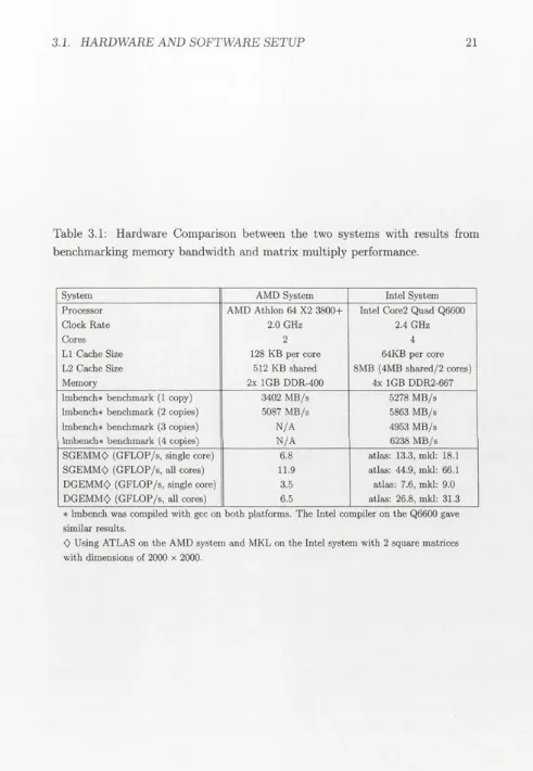
Benchmarks were performed on two systems. The first system, that also hosts the GeForce 8800 GTX GPU, is an AMD system containing a 2GHz dual core AMD Athlon64 3800+ processor with 2GB of PC3200 DDR memory. The processor has 128KB of LI cache, 1 MB of L2 cache and a theoretical peak performance of 8 GFLOP/s. The GPU is installed in a PCIe 1.0 slot with a peak theoretical bandwidth of 4GB/s.
While the processor in this system was acceptable at the start of this work, processors have improved markedly in the last 18 months. A new Intel system was added for comparison. This system is a Sun Ultra™ 24 Workstation with a Q6600 2.4 GHz Core2 Quad CPU (4 core, 8MB L2 cache, 1066MHz FSB) and 4 GB of DDR2-66T memory. Table 3.1 provides a comparison between the hardware of the two systems as well as the maximum memory bandwidth and single and double-precision FLOP/s achieved on both CPUs using matrix multiply routines.
Memory bandwidth evaluations between the host and the GPU were per-formed with host-side functions provided by the CUD A toolkit version 2.0. Dense matrix-vector products on the GPU were performed with the CUDA BLAS library version 2.0 (CUBLAS). ATLAS1 [59] version 3.6.0 and 3.8.2 in addition to Intel’s Math Kernel Library (MKL) version 10.0.1.014 were used for the dense matrix- vector products on the two CPUs. Both systems were dedicated for benchmarking and the wall clock time was used to measure the time for all the benchmarks. All benchmarks were run 100 times and results were averaged. FLOP/s were calculated as ((2 x M x TV) + time) where M and N are the dimensions of the matrix.
3.1
.HARDWARE AND SOFTWARE SETUP
21Table 3.1: Hardware Comparison between the two systems with results from
benchmarking memory bandwidth and matrix multiply performance.
System AMD System Intel System
Processor AMD Athlon 64 X2 3800+ Intel Core2 Quad Q6600
Clock Rate 2.0 GHz 2.4 GHz
Cores 2 4
LI Cache Size 128 KB per core 64KB per core
L2 Cache Size 512 KB shared 8MB (4MB shared/2 cores)
Memory 2x 1GB DDR-400 4x 1GB DDR2-667
lmbench* benchmark (1 copy) 3402 MB/s 5278 MB/s
lmbench* benchmark (2 copies) 5087 MB/s 5863 MB/s
lmbench* benchmark (3 copies) N/A 4953 MB/s
lrnbench* benchmark (4 copies) N/A 6238 MB/s
SGEMMO (GFLOP/s, single core) 6.8 atlas: 13.3, mkl: 18.1
SGEMMO (GFLOP/s, all cores) 11.9 atlas: 44.9, mkl: 66.1
DGEMM<> (GFLOP/s, single core) 3.5 atlas: 7.6, mkl: 9.0
DGEMMO (GFLOP/s, all cores) 6.5 atlas: 26.8, mkl: 31.3
* lmbench was compiled with gcc on both platforms. The Intel compiler on the Q6600 gave similar results.
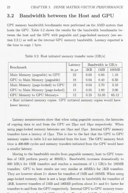
[image:28.536.33.524.32.742.2]3.2 Bandwidth between the Host and G PU
[image:29.536.45.479.47.698.2]GPU memory bandwidth benchmarks were performed on the AMD system that
hosts the GPU. Table 3.2 shows the results for the bandwidth benchmarks
be-tween the host and the GPU with pageable and page-locked memory (see
sec-tion 2.2.1) as well as the internal GPU memory bandwidth. Latency reported is
the time to copy 1 byte.
Table 3.2: Host initiated memory transfer rates (GB/s)
Benchmark
Latency
Bandwidth in GB/s
in
/is
1KB
1MB
100MB
Main Memory (pageable) to GPU
22
0.03
0.80
1.10
GPU to Main Memory (pageable)
18
0.04
0.40
0.50
Main Memory (page-locked) to GPU
18
0.04
2.70
3.10
GPU to Main Memory (page-locked)
15
0.05
2.80
3.00
GPU Memory to GPU Memory*
12
0.25
53.95
65.12
* Host initiated memory copies. GPU initiated memory copies would have
lower latency.
Latency measurements show that when using pageable memory, the latencies
of copying data to and from the GPU are 22
/is
and 18
ßs
respectively. When
using page-locked memory latencies are 18/is and 15
fis.
Internal GPU memory
transfers have a latency of 12
fis.
This is due to the fact that the GPU to GPU
memory copies in table 3.2 are initiated from the host. The GPU memory fetch
time is 400-600 cycles and memory transfers initiated from the GPU would have
a smaller latency.
3.3. DENSE MATRIX-VECTOR PERFORMANCE
23
bandwidth and a maximum of 65GB/s was achieved with 100MB transfers; this
is about 81% of peak theoretical performance.
Results from table 3.2 suggest that the page-locked memory should be used for
faster memory transfers. When using page-lock memory, data was able to move
at a maximum rate of 3GB/s between the host and the GPU with more than 85%
of this bandwidth being achieved with only 1MB transfers. This is about half the
bandwidth of main memory as presented in table 3.1. This limitation is a result
of the PCIe bus which has a theoretical limit of 4GB/s in each direction. All
newer GPUs support the newer PCIe 2.0 bus with a theoretical limit of 8GB/s in
each direction and the bandwidth between the GPU and host would be expected
to double. The low bandwidth between the GPU and host clarifies the large cost
of moving data to the GPU. In terms of the SML application, it indicates that
many iterations of matrix-vector products will be needed to offset the cost of the
initial matrix transfer. The cost of copying the vector and result between the
GPU and host for each matrix-vector product will need to be identified as well.
The large internal GPU bandwidth is about 31 x the internal bandwidth of the
host. This indicates an advantage for the GPU in memory bound computations
such as matrix-vector products.
Having quantified the cost of memory transfers between the host and the GPU,
the performance of dense matrix-vector products on the GPU are evaluated.
3.3 D ense M atrix-V ector Perform ance
This section, will discuss the results from evaluating the performance of single
precision, dense matrix-vector products using both dedicated matrix-vector
rou-tines (SGEMV) and matrix matrix rourou-tines (SGEMM) on the AMD and Intel
CPUs as well as the GPU. Both the SGEMV and SGEMM routines are used to
calculate the product of a NxM matrix with a Mxl vector.
Given a matrix of dimensions MxN, listing 3.1, illustrates a simple algorithm
for computing the matrix-vector products.
Listing 3.1: Structure of Dense Matrix-Vector Products
f o r ( i = 0 ; i < M ; i + + ) f o r ( j = 0 ; j < N ; j + + )
r e s [ i ] + = A [ i ] [ j ] * v e c [ j ) ;
optimal access method for both the GPU and CPU systems. On both AMD and
Intel CPUs, the matrix-vector products would be able to perform two operations
per one element of the matrix. This would allow us to achieve a peak performance
of
(bandwidth +
4
bytes
) x 2
operations
in GFLOP/s. From table 3.1, memory
bandwidth is seen to reach 6GB/s on both CPU systems. It is interesting to
see that both these processors, while generations apart give the same predictable
amount of performance for dense matrix-vector products due the similar memory
bandwidth performance.
The SML application includes a normal matrix-vector multiplication as well
as a transpose matrix-vector multiplication and therefore, both normal (N) and
transpose (T) options in the matrix-vector routines are evaluated. The
evalua-tions cover a range of different sizes and ratios between rows and columns.
In the performance analysis of matrix-vector products, the effect of the size
of the matrix on performance is observed as well as the shape of the matrix (ie.
the ratio of rows to columns). To observe the effect of these parameters, two
experiments are performed. In the first, matrix-vector products are evaluated
with square matrices of ascending sizes and in the second, the size of a matrix is
kept constant and the ratio between the number of rows to the number of columns
is modified. In addition, to factor in the per iteration overheads of data transfers
between host and GPU, the results for the GPU include the time required to
transfer the vector to the GPU and the resulting product vector back to the host.
Performance for SGEMM and SGEMV calls performing matrix-vector
prod-ucts will be given for the CPUs and the GPU. A range of matrix sizes from 1024
to 10240 with increments of 128 are tested. The results are provided for both
normal and transpose multiplications. ATLAS and MKL permit the matrix to be
stored in either row or column major format, while CUDA only supports
matri-ces in column major format. All evaluations are therefore conducted on matrimatri-ces
stored in columns major format.
3.3.1 Effect of Size on D ense M atrix-Vector Perform ance
The first set of performance results for SGEMM and SGEMV are for the AMD
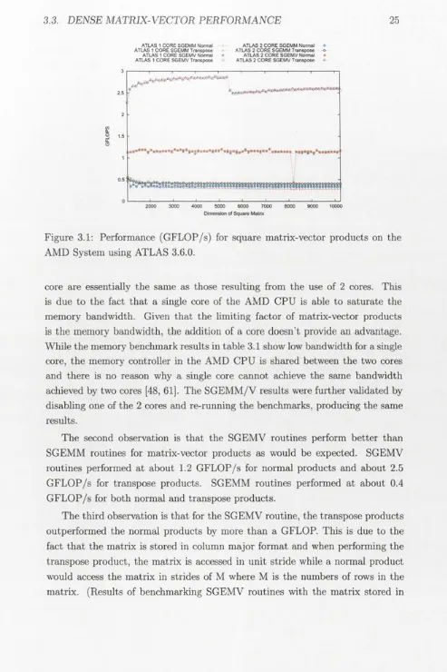
CPU and are presented in figure 3.1 and partially replicated in table 3.3. A
variety of matrix sizes from 1024 to 10240 with increments of 128 are shown.
Since ATLAS 3.6.0 performed best on the AMD system, only those results are
presented.
3.3. DENSE MATRIX-VECTOR PERFORMANCE
25
ATLAS 1 CORE SGEMM Normal ATLAS 2 CORE SGEMM Normal • ATLAS 1 CORE SGEMM Transpose ATLAS 2 CORE SGEMM Transpose
-©•-ATLAS 1 CORE SGEMV Normal * ATLAS 2 CORE SGEMV Normal • ATLAS 1 CORE SGEMV Transpose ATLAS 2 CORE SGEMV Transpose
•»**, i , » * * M H " , * i* t* ;* » * * , **, *, « j * i t ' , t ‘ * ‘ i* * '» * « » M * » » * •$ « , *»»*««»*• I
5000 6000 7000 Dimension of Square Matrix
10000
Figure 3.1: Performance (GFLOP/s) for square matrix-vector products on the
AMD System using ATLAS 3.6.0.
core are essentially the same as those resulting from the use of 2 cores. This
is due to the fact that a single core of the AMD CPU is able to saturate the
memory bandwidth. Given that the limiting factor of matrix-vector products
is the memory bandwidth, the addition of a core doesn’t provide an advantage.
While the memory benchmark results in table 3.1 show low bandwidth for a single
core, the memory controller in the AMD CPU is shared between the two cores
and there is no reason why a single core cannot achieve the same bandwidth
achieved by two cores [48, 61]. The SGEMM/V results were further validated by
disabling one of the 2 cores and re-running the benchmarks, producing the same
results.
The second observation is that the SGEMV routines perform better than
SGEMM routines for matrix-vector products as would be expected. SGEMV
routines performed at about 1.2 GFLOP/s for normal products and about 2.5
GFLOP/s for transpose products. SGEMM routines performed at about 0.4
GFLOP/s for both normal and transpose products.
[image:32.536.33.526.50.790.2]row major format produced the the same results only with the normal products performing in the 2.5 GFLOP/s range and the transpose products performing in the 1.2 GFLOP/s range.)
The final observation is that the performance of ATLAS routines are very consistent across a variety of different sized matrices.
Table 3.3: Performance in GFLOP/s for square matrix-vector products on the AMD System using ATLAS v3.6.0 (see figure 3.1).
Performance in GFLOP/s
Dimension 1 Thread 2 threads
SGEMM SGEMV SGEMM SGEMV
N T N T N T N T
1024 0.47 0.58 1.13 2.28 0.46 0.54 1.12 2.27
2048 0.33 0.43 1.18 2.80 0.36 0.41 1.18 2.80
3072 0.32 0.40 1.19 2.82 0.36 0.42 1.20 2.84
4096 0.31 0.39 1.15 2.86 0.35 0.42 1.18 2.85
5120 0.30 0.39 1.20 2.86 0.35 0.42 1.20 2.84
6144 0.29 0.38 1.20 2.52 0.35 0.41 1.17 2.52
7168 0.29 0.37 1.21 2.56 0.35 0.41 1.20 2.57
8192 0.27 0.37 0.43 2.57 0.34 0.40 0.43 2.61
9216 0.28 0.38 1.18 2.60 0.34 0.41 1.17 2.59
10240 0.28 0.37 1.16 2.56 0.34 0.41 1.17 2.61
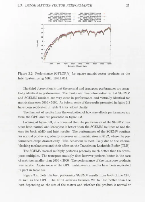
The next set of results provided are for the Intel system, where the same experiments conducted on the AMD system are repeated. The Intel MKL library performed best on this system so only the MKL results are shown. The Intel system has four cores and so results are provided from the utilisation of one, two and four cores.
The first observation in figure 3.2 is that again, there is no noticeable per-formance increase due to the involvement of multiple cores in the matrix-vector product. For the Intel system, this was indicated by the memory benchmark results in table 3.1 where the results for one core were over 80% of what was achieved with four cores.
3.3. DENSE MATRIX-VECTOR PERFORMANCE
27MKL 1 CORE SGEMM Normal MKL 1 CORE SGEMM Transpose
MKL 1 CORE SGEMV Normal * MKL 1 CORE SGEMV Transpose
MKL 2 CORE SGEMM Normal • MKL 2 CORE SGEMM Transpose o
MKL 2 CORE SGEMV Normal • MKL 2 CORE SGEMV Transpose *
MKL 4 CORE SGEMM Normal MKL 4 CORE SGEMM Transpose
MKL 4 CORE SGEMV Normal r MKL 4 CORE SGEMV Transpose «
5000 6000 7C Dimension of Square Matrix
10000
Figure 3.2: Performance (GFLOP/s) for square matrix-vector products on the Intel System using MKL 10.0.1.014.
The third observation is that the normal and transpose performance are essen-tially identical in performance. The fourth and final observation is that SGEMV and SGEMM routines are very close in performance and virtually identical for matrix sizes over 5000 x 5000. As before, some of the results presented in figure 3.2 have been replicated in table 3.4 for added clarity.
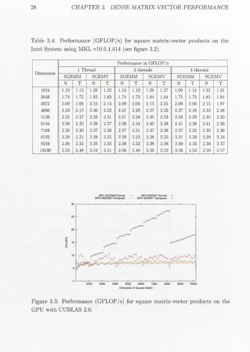
The final set of results from the evaluation of how size affects performance are from the GPU and are presented in figure 3.3.
Looking at figure 3.3, it is observed that the performance of the SGEMV rou-tines both normal and transpose is better than the SGEMM rourou-tines as was the case for both AMD and Intel results. The performance of the SGEMV routines for normal products gradually increases until matrix sizes of 8192, where the per-formances drops dramatically. This behaviour is most likely due to the internal blocking mechanisms and their affect on the Translation Lookaside Buffer (TLB).
The SGEMV normal multiply performs generally much better than the trans-pose multiplies. The transtrans-pose multiply does however perform better in the case of matrices smaller than 2000 x 2000. The performance of the transpose products was erratic. Again some of the GPU matrix-vector results have been replicated in part in table 3.5.
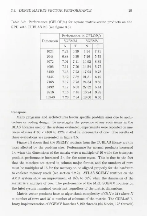
[image:34.536.18.528.53.762.2]Table 3.4: Performance (GFLOP/s) for square matrix-vector products on the
Intel System using MKL vlO.0.1.014 (see figure 3.2).
P erform ance in G F L O P /s
D im ension 1 T h re a d 2 th re a d s 4 th re a d s SG EM M SG E M V SG EM M S G E M V SG EM M SG E M V
N T N T N T N T N T N T
1024 1.10 1.13 1.28 1.32 1.13 1.13 1.28 1.27 1.09 1.14 1.32 1.31 2048 1.74 1.72 1.83 1.83 1.74 1.73 1.84 1.84 1.75 1.73 1.85 1.84 3072 2.09 2.06 2.15 2.14 2.09 2.06 2.15 2.15 2.09 2.06 2.15 1.97 4096 2.23 2.15 2.26 2.22 2.21 2.20 2.27 2.25 2.27 2.19 2.32 2.28 5120 2.25 2.27 2.33 2.31 2.31 2.28 2.35 2.33 2.33 2.29 2.35 2.33 6144 2.38 2.32 2.39 2.37 2.39 2.34 2.40 2.38 2.41 2.36 2.41 2.39 7168 2.26 2.30 2.37 2.36 2.37 2.31 2.37 2.36 2.37 2.32 2.39 2.36 8192 2.28 2.21 2.29 2.25 2.30 2.22 2.28 2.25 2.31 2.20 2.28 2.24 9216 2.36 2.32 2.35 2.35 2.38 2.32 2.38 2.36 2.39 2.33 2.39 2.37 10240 2.53 2.48 2.54 2.51 2.56 2.48 2.56 2.52 2.56 2.53 2.59 2.57
GPU SGEMM Normal GPU SGEMV Normal * GPU SGEMM Transpose GPU SGEMV Transpose o
5000 6000 71 Dimension of Square Matrix
10000
[image:35.536.9.506.58.757.2]3.3. DENSE MATRIX-VECTOR PERFORMANCE
29
Table 3.5: Performance (GFLOP/s) for square matrix-vector products on the
GPU with CUBLAS 2.0 (see figure 3.3).
Dimension
Performance in GFLOP/s
SGEMM
SGEMV
N
T
N
T
1024
7.23 6.39
4.54
7.71
2048
6.88 6.30
7.26
5.75
3072
7.01 7.11 10.92 8.85
4096
7.11 7.20 14.54 5.77
5120
7.13 7.23 17.94 9.78
6144
7.12 7.32 21.31 6.19
7168
7.17 7.73 24.34 9.80
8192
7.17 6.33 27.32 5.44
9216
7.16 7.45 16.24 9.28
10240
7.20 7.84 18.00 6.05
transpose.
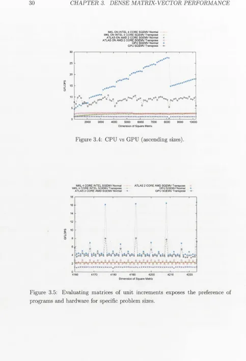
Many programs and architectures favour specific problem sizes due to
archi-tecture or coding design. To investigate the presence of any such issues in the
BLAS libraries used or the systems evaluated, experiments were repeated on
ma-trices of sizes 4160 x 4160 to 4224 x 4224 in increments of one. The results of
these evaluations are presented in figure 3.5.
Figure 3.5 shows that the SGEMV routines from the CUBLAS library are the
most affected by the problem size. Performance for normal products increased
4x when the dimensions of the matrix were a multiple of 16 while the transpose
product performance increased 2x for the same cases. This is due to the fact
that the matrices are stored in column major format and the numbers of rows
must be multiples of 16 for the memory to be aligned properly for the hardware
to coalesce memory reads (see section 2.2.2). ATLAS SGEMV routines on the
AMD system show an improvement of 15% to 50% when the dimension of the
matrix is a multiple of two. The performance of the MKL SGEMV routines on
the Intel system remained consistent regardless of the matrix dimensions.
[image:36.536.44.521.37.740.2]MKL ON INTEL 4 CORE SGEMV Normal MKL ON INTEL 4 CORE SGEMV Transpose
ATLAS ON AMD 2 CORE SGEMV Normal * ATLAS ON AMD 2 CORE SGEMV Transpose
GPU SGEMV Normal • GPU SGEMV Transpose
-©•-_ iijo m o < M B e e B B G p e g s ia s g v B B y e 'i ! a r t a y i ^ aB iB a a BirglffiBg,B Ma B B a B a ia a flia B e B B BIi1^ Bg iiiir .B i!.» i
5000 6000 7( Dimension of Square Matrix
10000
Figure 3.4: CPU vs GPU (ascending sizes).
MKL 4 CORE INTEL SGEMV Normal ATLAS 2 CORE AMD SGEMV Transpose MKL 4 CORE INTEL SGEMV Transpose GPU SGEMV Normal •
ATLAS 2 CORE AMD SGEMV Normal « GPU SGEMV Transpose
o-\ m ° ? i : f> \ O ;
■£ÖöQ5so S ® 5'\°8 8 *I'Q£&8 8 % Q8*8 8^5a6&3 q*^q‘gS'
8 g 8
1 ******** h******-*-*-*-*-^**-*-*-**-*-*-*-***********)**-*-*-*-*-*-***».,, ***** * ****
4170 4190 4200 Dimension of Square Matrix
[image:37.536.13.496.66.775.2]3.3. DENSE MATRIX-VECTOR PERFORMANCE
31
each looping over as many rows as needed to compute all rows. For given
M
we
would expect the performance of the SGEMV routine to peak when
N
is a
mul-tiple of 8,192 due to maximum utilisation of all threads. The performance should
increase linearly as
N
approaches a multiple of 8,192. Figure 3.3 shows that the
performance of the SGEMV routine does indeed scale linearly with respect to
N
and peaks at
N =
8,192. The performance drops drastically after that due to
poor utilisation as a total of 16,384 threads would have been created but only
8,193 of them would contribute work. As
N
increases, the performance starts to
ascend linearly to another maximum (expected) at
N =
16,384.
3.3.2 Effect of Shape on Perform ance
The effect of matrix shape on performance of the SGEMV routines from the
ATLAS, MKL and CUBLAS libraries, was evaluated using a matrix containing
26,214,400 elements (approximately 100MB in size). Keeping the number of
elements of the matrix constant, the number of rows and columns are varied
from a 128 x 204800 matrix to 204800 x 128. Figure 3.6 presents the results of
the evaluations of the two CPUs. Only results for the the SGEMV routines are
presented for both CPUs as they consistently outperform the SGEMM routines.
Figure 3.7 presents the results of both SGEMV and SGEMM GPU routines as
neither of them consistently outperforms the other. Results are also partially
replicated in table 3.6 for further clarification.
MKL 4 CORE INTEL SGEMV Normal ATLAS 2 CORE AMD SGEMV Normal *
MKL 4 CORE INTEL SGEMV T ranspose ATLAS 2 CORE AMD SGEMV T ranspose
2 1-5
10000 0.0001
Rows/Columns
Starting with the results of the MKL SGEMV routine on the Intel system
presented in figure 3.6, both normal and transpose products showed a small drop
in performance when the number of rows or columns dropped to 128. The normal
products saw an increase in performance form small number of columns, while the
transpose products saw an increase for small number of rows. The ATLAS normal
SGEMV results lagged the transpose SGEMV results by almost 1.5 GFLOP/s
for most of the test cases. A small decrease in performance is observed for small
number of rows and a much higher drop of 50% is observed at matrices of sizes
8192 x 3200, 16384 x 1600 and 204800 x 128. The ATLAS transpose SGEMV
results were not affected by a small number of rows but show a significant drop
in performance for a small number of columns.
Generally the results indicate that the performance of the MKL
implemen-tation on the Intel CPU is more stable than the ATLAS results on the AMD
CPU. However, the ATLAS SGEMV results on the AMD CPU produce better
performance than the MKL implementation on the Intel CPU when the matrix is
read in unit stride (row major + normal products or column major 4- transpose
products ) and much worse than the MKL implementation on the Intel CPU
when they are not.
GPU SGEMM Normal GPU SGEMV Normal * GPU SGEMM Transpose GPU SGEMV Transpose
.. . m j b j j k * * # * * -'* :S--- t
0.0001 10000
Rows/Columns
Figure 3.7: Performance (GFLOP/s) as function of shape for matrix-vector
prod-uct on the GPU.
3.3. DENSE MATRIX-VECTOR PERFORMANCE
33The SGEMV transpose results are not as stable with a drop of 50% in perfor-mance showing for some matrices. The SGEMV transpose products also drops in performance for small number of rows. The SGEMV normal product performs much worse than the others for number of rows under 2048 after which perfor-mance increases rapidly. There is a sharp drop in perforperfor-mance for the matrix of size 10240 x 2560 but performance levels out as the number of rows continues to grow. An important observation is that for small number of rows, the use of SGEMM routines will perform better than SGEMV routines.
Table 3.6: Performance (GFLOP/s) as function of shape for matrix-vector prod-ucts on the CPU (see figures 3.6 and 3.7).
Rows Columns
AMD Intel GPU
SGEMV SGEMV SGEMM SGEMV
N T N T N T N T
128 204800 0.99 2.59 1.67 1.87 1.70 1.95 0.65 1.29
512 51200 1.22 2.58 2.13 2.24 6.97 7.06 2.23 5.11
1024 25600 1.28 2.58 2.60 2.23 7.13 7.49 3.76 9.77
1600 16384 1.24 2.55 2.62 2.23 5.60 4.93 7.18 4.44
2048 12800 1.23 2.48 2.55 2.40 7.16 7.79 7.54 9.66
2560 10240 1.18 2.62 2.56 2.26 7.15 7.23 10.65 5.79
3200 8192 1.19 2.60 2.50 2.24 6.43 5.41 13.48 5.61
4096 6400 1.16 2.51 2.32 2.43 7.14 7.75 14.64 9.33
5120 5120 1.20 2.88 2.33 2.31 7.13 7.20 17.94 9.78
6400 4096 1.15 2.60 2.43 2.34 6.87 7.18 23.14 5.57
8192 3200 0.44 2.84 2.23 2.50 7.12 7.73 26.75 9.40
10240 2560 1.17 2.83 2.24 2.58 7.13 7.51 17.71 9.71
12800 2048 1.11 2.54 2.35 2.55 7.15 7.25 21.99 6.03
16384 1600 0.46 2.74 2.20 2.61 7.09 7.87 26.60 9.68
25600 1024 1.15 2.57 2.26 2.64 7.25 7.74 21.37 9.75
51200 512 1.19 2.37 2.24 2.13 7.14 7.68 23.74 9.71
204800 128 0.46 1.55 1.70 1.68 6.51 6.72 22.70 9.09
Finally, figure 3.8 combines SGEMV performance results for the AMD and Intel CPU with the results from the GPU.
MKL 4 CORE INTEL SGEMV Normal ATLAS 2 CORE AMD SGEMV Transpose
MKL 4 CORE INTEL SGEMV Transpose GPU SGEMV Normal •
ATLAS 2 CORE AMD SGEMV Normal * GPU SGEMV T ranspose o
-9---P-D S' g 'd ? -9 f t
0.0001 10000
[image:41.536.18.492.66.746.2]Rows/Columns
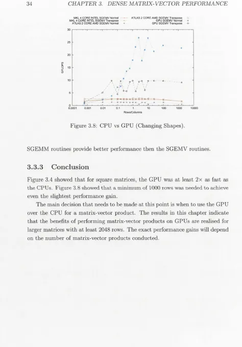
Figure 3.8: CPU vs GPU (Changing Shapes).
SGEMM routines provide better performance then the SGEMV routines.
3.3.3 Conclusion
Figure 3.4 showed that for square matrices, the GPU was at least 2x as fast as
the CPUs. Figure 3.8 showed that a minimum of 1000 rows was needed to achieve
even the slightest performance gain.
C h ap ter 4
SpM V C on stru ctio n and
E valuation
As noted in chapter 2, exploiting the sparsity of a matrix can decrease the number
of instructions needed to compute a matrix-vector product as well as the memory
footprint of the matrix. This exploitation also introduces a slightly more complex
data structure and random memory accesses. The point at which the sparsity
of a matrix becomes large enough to benefit from its exploitation is system and
implementation dependent. This chapter presents a range of implementation
options on the NVIDIA GPU system, assesses their performance as a function
of matrix attributes, and by doing so establishes a set of implementations such
that for any matrix the best performing implementation is part of that set. This
chapter also presents efforts to identify the level of sparsity that warrants the use
of sparse matrix-vector products on the GPU over their dense counterparts.
There are many storage formats for sparse matrices as discussed in section 2.4.
This work is based on the Compressed Sparse Row (CSR) format as it is widely
used in the scientific community [52, 56, 13].
________Listing 4.1: Structure of CSR Sparse matrix-vector products_______
f o r ( i = 0 ; i < M ; i + + )
f o r ( j = p t r [ i ] ; j < p t r [ i + 1 ) ; j + + )
r e s [ i ] + = v a l [ j ] » v e c [ i n d [ j ] ] ;