optical transitions in the valence band by internal photoemission spectroscopy
.
White Rose Research Online URL for this paper:
http://eprints.whiterose.ac.uk/78951/
Version: Published Version
Article:
Lao, Y-F, Perera, AGU, Li, LH et al. (3 more authors) (2013) Direct observation of spin-orbit
splitting and phonon-assisted optical transitions in the valence band by internal
photoemission spectroscopy. Physical Review B: Condensed Matter and Materials
Physics, 88 (20). 201302. ISSN 1098-0121
https://doi.org/10.1103/PhysRevB.88.201302
eprints@whiterose.ac.uk https://eprints.whiterose.ac.uk/ Reuse
Unless indicated otherwise, fulltext items are protected by copyright with all rights reserved. The copyright exception in section 29 of the Copyright, Designs and Patents Act 1988 allows the making of a single copy solely for the purpose of non-commercial research or private study within the limits of fair dealing. The publisher or other rights-holder may allow further reproduction and re-use of this version - refer to the White Rose Research Online record for this item. Where records identify the publisher as the copyright holder, users can verify any specific terms of use on the publisher’s website.
Takedown
If you consider content in White Rose Research Online to be in breach of UK law, please notify us by
Direct observation of spin-orbit splitting and phonon-assisted optical transitions
in the valence band by internal photoemission spectroscopy
Yan-Feng Lao and A. G. Unil Perera*
Department of Physics and Astronomy, Georgia State University, Atlanta, Georgia 30303, USA
L. H. Li, S. P. Khanna,†and E. H. Linfield
School of Electronic and Electrical Engineering, University of Leeds, Leeds LS2 9JT, United Kingdom
H. C. Liu
Key Laboratory of Artificial Structures and Quantum Control, Department of Physics and Astronomy, Shanghai Jiao Tong University, Shanghai 200240, China
(Received 30 January 2013; published 11 November 2013)
We employ internal photoemission spectroscopy to directly measure the valence-band Van Hove singularity, and identify phonons participating in indirect intervalence-band optical transitions. Photoemission of holes photoexcited through transitions between valence bands displays a clear and resolvable threshold, unlike previous reports of interband critical points which become obscure in doped materials. We also demonstrate the enhancement of optical phonon-assisted features primarily contributing to the photoemission yield. This result is evidence of the relaxation of photoexcited hot holes through intravalence-band scatterings in heterojunctions, which contrast with intervalence-band scatterings in bulks.
DOI:10.1103/PhysRevB.88.201302 PACS number(s): 78.30.Fs, 71.70.Ej, 73.40.Kp, 79.60.Jv
Optical studies of light interacting with a material reveal fundamental information about its electronic structure, photons, phonons, and carrier dynamics in the material,inter alia.1–4 Many fundamental studies and device applications make use of optical transitions between different energy bands,5–11 among which the valence-to-conduction band (VB to CB) transitions are typically used to determine band parameters,9 e.g., the interband Van Hove singularities.10 Despite the well-known electronic structure, understanding of VB-related physics is still very limited. Nearly all of what is currently understood about VBs come from optical absorption5–7and interband transition-based experiments,9,10 the latter of which encounters a fundamental difficulty when band tailing perturbed obscuring effects dominate.12 This limitation makes it impossible to measure the VB singularity on the basis of free-carrier effects. Aside from this, although many theoretical studies on free-carrier absorption are reported,13,14the determination of the dominant contributions to the carrier-phonon coupling in indirect intervalence-band (IVB) transitions is yet to be demonstrated experimentally.
In this Rapid Communication, we demonstrate that internal photoemission (IPE) of holes at a heterojunction interface provides a direct characterization of the valence-band and hole dynamics. Of the various optical processes illustrated in Fig. 1(a), indirect transitions take place either through an intermediate state lying in the VB from which the transition originates, or through a nearby band. On the contrary to readily observing phonons associated with inter-band absorption in indirect-gap semiconductors,16identifying phonons participating in indirect IVB transitions is impossible through optical absorption, according to its featureless profile [Fig. 1(b)] and also extensive absorption data reported in past literature.7 IPE occurs at the junction interface when the kinetic energies of photoexcited carriers in the photon absorber (emitter) are sufficiently higher than the barrier.17For
successful photoemission, photocarriers must transfer between the energy bands of the absorber and barrier, which leads to remarkable features associated with indirect transitions due to their higher probabilities of occurring compared to direct transitions.18Analysis of the IPE results also allows us to study hole dynamics upon photoexcitation. Our results broaden the understanding of the VBs and optical processes, which, for example, may offer a better understanding of the origin of hole-mediated ferromagnetism for p-type (Ga,Mn)As,19 by distinguishing IVB transitions from impurity band-to-valence band transitions through resolving the VB singularity. In addition to this fundamental interest, phonon identification will find applications in determining free-carrier absorption, an important source of modal loss in light-emitting and laser devices.13,14
The IPE quantum yield (Y)17is obtained asY =(I /P)hν, where I is the photocurrent of the sample, and P is the power of incident light. A commercial bolometer with known sensitivity was used to measure P for spectral calibration. Photocurrent spectra were acquired by mounting the sample in a liquid-helium dewar and using a Perkin-Elmer system 2000 Fourier transform infrared (FTIR) spectrometer. The sample for IPE studies uses emitter/barrier heterojunctions (e.g.,
p-type doped GaAs/undoped AlGaAs).20 Although IPE was reported more than four decades ago,21 it remains attractive, as recently demonstrated for characterizing materials such as graphene and oxide-based structures.22 Here, going beyond the standard focus on obtaining band offsets,17,21we illustrate an exploration of IPE to study the VB structure and related optical processes.
Features of hole photoemission solely associated with the
p-type GaAs emitter are confirmed by IPE of samples with different AlxGa1−xAs barriers, as shown in Fig.1(c). Except
LAO, PERERA, LI, KHANNA, LINFIELD, AND LIU PHYSICAL REVIEW B88, 201302(R) (2013)
0 5
1×1019cm−3
3×1018cm−3 p-type GaAs
(b)
Wavelength (μm)
12 9 6 3
Quantum
yield
(a.
u.)
Photon energy (eV)
0.1 0.2 0.3 0.4 0.5 0.6 0.7
D (-0.5V) A (6V) B (6V) C (6V) (c) 80K
HH→SO HH→LH
¯ hω3 Phonon ¯ hω 4 Ener gy Band edge Ef EB HH LH SO
k〈111〉 k〈100〉
(1)
(2) (3) (4)
(5)
¯ hω2
¯
hω1
(a) A B C D 0.15 eV 0.22 eV 0.32 eV 0.32 eV 0. 42 eV 0. 25 eV (1 0
3 cm
-1)5
FIG. 1. (Color online) (a) Schematic of various intervalence-band (IVB) optical transitions, where (1)–(5) have the following meanings: (1) Direct IVB transition; (2) IVB transition+phonon emission (¯hω1); (3) phonon absorption (¯hω2)+IVB transition;
(4) IVB transition+phonon emission (¯hω3) (interband scattering);
and (5) phonon absorption (¯hω4)+intraband photon absorption. The
inset shows the photon excitation and emission of a hole in an emitter (E)/barrier (B) heterojunction. It was found that transition (2) has a dominant contribution to the photoemission yield. (b) Optical absorption (α) ofp-type GaAs. (c) Internal-photoemission spectra of p-type GaAs/AlxGa1−xAs heterojunctions. The inset illustrates
the flat-band (VB) diagrams (Ref. 15) at zero bias. The shaded area schematically shows the Fermi level of the emitter [doping concentration: 3×1018cm−3(A, B, and C) and 1×1019cm−3(D)].
The photon energy ranges where the HH→LH or HH→SO transitions dominate are indicated. The features indicated by vertical arrows remain the same in different samples.
and 0.45 eV have very similar profiles between different samples. The undulations beyond 0.45 eV (samples A–C) result from optical interference which can be clarified by optical calculations. The sharp peak of sample A at 0.193 eV was previously interpreted as LH-HH spin-orbit splitting (LH and HH denote the light- and heavy-hole band, respectively).11 The variation in the applied bias is to adapt to the differences in the structures between samples to obtain optimum spectra. However, the features between 0.3 and 0.45 eV barely depend on bias, as well as the barrier height and shape (affected by bias-induced image-force barrier lowering17). In comparison with absorption [Fig. 1(b)], these features likely originate from the HH→SO hole transitions. Interband transitions and lattice absorption as the causes can be excluded, as they occur only in even higher- and lower-energy ranges, respectively. Transitions originating from the impurity band can also be excluded, because the impurity band is already merged with the VB for doping concentration of>3×1018cm−3
.8Moreover, the intravalence-band transition is insignificant for this spectral range. This leaves the intervalence-band transitions as the only mechanism for interpreting the features.
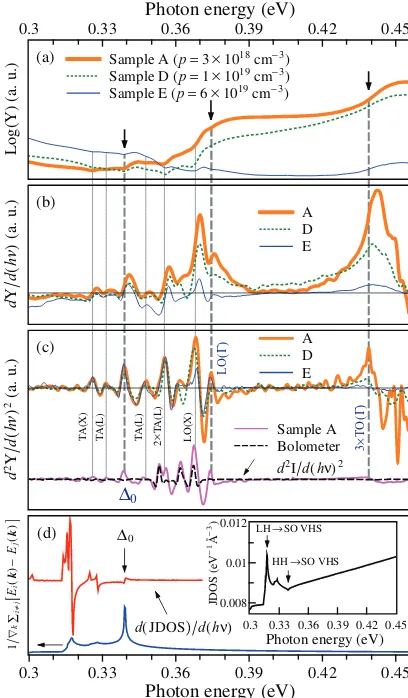
In order to examine the features in more detail, we differentiated quantum yield spectra [Figs. 2(a)–2(c)]. The peaks in the double differential plots correspond to the onsets of these features, and are thus used to determine thresholds of various transitions. It is tempting to interpret the second derivative peak at∼0.34 eV as correlated with the HH→SO singularity, corresponding to the band splitting gap at the
Ŵ point (0). This assertion is clarified by calculating
Log(Y)
(a.
u.)
Photon energy (eV)
0.3 0.33 0.36 0.39 0.42 0.45
(a) Sample A (p=3×1018cm−3)
Sample D (p=1×1019cm−3)
Sample E (p=6×1019cm−3)
d Y d ( h ν ) (a.
u.) (b) A
D E 1 k ∑i ≠ j Ei ( k )− Ej ( k )
Photon energy (eV)
0.3 0.33 0.36 0.39 0.42 0.45
(d) Δ0
d(JDOS d(hν)
JDOS (eV − 1Å − 3) 0.008 0.01 0.012
Photon energy (eV) 0.3 0.33 0.36 0.39 0.42 0.45
LH→SO VHS
HH→SO VHS
d 2Y d ( h ν ) 2(a. u.) Δ0 TA (L) TA (L) LO(X) 3 × TO ( Γ ) (c) TA (X) 2 × TA (L) LO( Γ ) A D E Sample A Bolometer
d2Id(hν)2
FIG. 2. (Color online) Comparison of (a) quantum yield (Y), and its (b) first and (c) second derivatives for samples A (6 V, 80 K), D (−0.5 V, 80 K), and E (0.05 V, 50 K). The structure of sample E is the same as A, except for its emitter doping concentration (6×1019cm−3). The vertical lines indicate the identified phonon
features (TableI). Also shown in (c) are the second derivatives of the as-measured sample and bolometer (background) spectra. (d) Calcu-lated 1/∇ki=j[Ei(k)−Ej(k)] by ak·pmodel (Ref.23) to show the
Van Hove singularities (VHS) of intervalence-band transitions, two of which are indicated in the inset. Also shown is the derivative of JDOS.
1/∇k
i,j[Ei(k)−Ej(k)] to show the singularities, and the
joint density of states (JDOS), as illustrated in Fig.2(d). The quantum yield can be expressed as17
Y(hν)∼
∞
−hν
ρ(ǫ,Ef)f(ǫ)P(ǫ+hν,)dǫ, (1)
where ρ and P are the energy distribution of photoexcited holes and their escape probability, respectively. Ef is the
Fermi level. f(ǫ) is the Fermi-Dirac distribution function. As f and P are slowly varying functions (in the energy regime around 0), we take the dominant contribution of
ρ for calculating derivatives, i.e.,dY /d(hν)∼ρ(−hν,Ef),
and henced2Y /d(hν)2∼d(JDOS)/d(hν), whereρ takes the
line shape of JDOS if only direct IVB transitions are consid-ered. The LH→SO transition exhibits a strong saddle-point singularity but cannot be observed because of the lower hole occupancy in the LH band. Due to its three-dimensional nature
[image:3.608.333.537.71.420.2] [image:3.608.54.294.75.217.2]0
(eV)
0.334 0.336 0.338 0.34 0.342
Temperature (K)
0 50 100 150 200 250 300
[image:4.608.52.295.71.157.2]p= 3 × 1018cm−3 p= 1 × 1019cm−3 p= 6 × 1019cm−3 Table III of Ref. 25
d
2Y
d
(
h
ν
)
2(a.
u.)
Photon energy (eV)
0.3 0.35 0.4 0.45
Sample D (-0.5V)
5.3K 40K 50K (a)
(b)
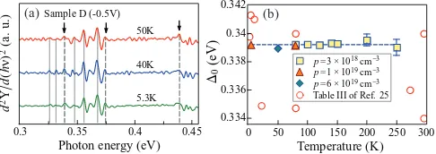
FIG. 3. (Color online) (a) Second yield derivative spectra of sample D at different temperatures. Results at different biases are similar and thus not shown here. Vertical lines indicate the identified phonon features. (b) Temperature and doping dependence of0for
GaAs which nearly remain constant (dashed line). Data of0adopted
from Table III of Ref.25are shown for comparison.
(dipole forbidden at Ŵ), the HH→SO singularity shows a weak signature in d(JDOS)/d(hν), in consistence with the experimental feature ofd2Y /d(hν)2. As shown in Fig.2(c),
a quite smooth as-measured bolometer spectrum around 0
justifies this result as not due to the background.
Typically,0wasindirectlydetermined10,24through resolv-ing interband critical points (atŴ):E0(HH to CB transitions) andE0+0(SO to CB).Directdetermination of0enables the study of its dependence on the doping concentration (Fig.2) and temperature [Fig.3(a)]. The determined values plotted in Fig.3(b)indicate that0nearly remains unchanged, and has an average of 0.3392±0.0003 eV, in reasonable agreement with reported values which are believed to be closer to 0.390–0.341 eV.26,27While the temperature dependency of0 can be readily obtained from interband transitions of undoped GaAs, it is difficult to determine the doping dependency,12 as band tailing significantly perturbs the density of states (DOS) at Ŵ. It can be deduced according to the two-thirds rule [1=(2/3)0],28that0remains constant, as interband critical points E1 (HH to CB) andE1+1 (LH to CB) (at
larger k) synchronously vary with doping concentrations.29 Our experiment is a direct justification of this result.
Band tailing introduces extended states in both the CB and VB, notably causing a reduction of the effective band gap.
Likewise, the expected reduction of the SO-HH splitting gap would be about 13 meV forp=1×1019cm−3. However,
stationary0 is confirmed in this study, indicating that0
is free of the shrinkage due to carrier-induced exchange and correlation effects30 as in the band gap. The unaltered HH→SO singularity may originate from transitions through localized states owing to dopants caused potential fluctua-tions. This supports the rigidity of the VBs, of which only the temperature rigidity has been studied previously.31 Our findings justify the rigid-band argument for studies, such as understanding doping-induced band gap narrowing effects and band alignment of doped heterojunctions.17
Returning to the phonon study, we identify phonons participating in IVB transitions based on yield spectra, and use the second derivatives to determine their energies. The possibility for the occurrence of indirect transitions is partially supported by observing a nonvanishing yield around 0. Calculations14 have shown enhanced absorption by over an order of magnitude, as a consequence of diverted transitions at largekpoints (dipole allowed) tok=0 (dipole forbidden) where the hole occupation is very strong. The participation of phonons plays an important role in this process; each of them results in an individual threshold being resolved. Noticing that IVB absorption is broad and featureless [Fig. 1(b)], the featured yield is thus a result of enhancement due to phonon-assisted transitions. The strongest features at∼0.37 and 0.44 eV [Fig.2(a)], which can be exclusively distinguished compared to the background [Fig.2(c)], are assigned with the energies of0+Eph, i.e., correlating with phonons: LO(Ŵ) and 3×TO(Ŵ) (Ephis the phonon energy). It was found that, as shown in Fig.2(a), these two features diminish as the emitter doping concentration increases to a higher level (sample E). Enhanced scatterings by charged impurity centers, as observed in the broadening of HH→SO absorption,7may alleviate the carrier-phonon coupling and cause yield reduction. Such an effect is in support of observed phonon features.
[image:4.608.52.560.584.712.2]Identification of other phonons associated with relatively weaker features may need good differentiation between the sample and background signal. As shown in Fig.2(c), the only suspicious feature is LO(X). Although this is also shown in
TABLE I. IPE features associated with phonons of GaAs (80 K).0is the HH-SO spin-orbit splitting energy with a value of 339.2±0.3 meV.
The energies of single phonons are the averages of values from different samples measured at different experimental conditions. The numbers in parentheses are uncertainties.
Features (meV) 0−13.0 0−7.4 0 0+8.7 0+16.3
Phonons TA(X) TA(L) TA(L) 2×TA(L)
Features (meV) 0+28.9 0+35.4 0+99.4
Phonons LO(X) LO(Ŵ) 3×TO(Ŵ)
TO(Ŵ) LO(Ŵ) LO(X) TA(X) TA(L)
This work (meV) 33.1(0.2) 35.4(0.2) 28.9(0.2) 12.2(0.8) 8.1(0.5) Waughet al.a 33.2(0.3) 35.4(0.8) 29.9(0.6) 9.75(0.06) 7.70(0.06)
Blakemoreb 33 35.5 30 8
Giannozziet al.c 33.6 36.1 29.8 10.2 7.8
Steigeret al.d 33.2 36.1 28.9 8.9 8.8
aReference32.
bExtracted from multiple phonon assignment to reststrahlen absorption peaks; see Table XI of Ref.27. cReference33.
LAO, PERERA, LI, KHANNA, LINFIELD, AND LIU PHYSICAL REVIEW B88, 201302(R) (2013)
the as-measured background spectrum, its existence cannot be ruled out as its normalized intensity is much higher than that of the background. Various phonons that were determined are shown in TableI. High-energy phonon features are interpreted as multiples of the same phonon rather than a combination of different phonons, as this assignment gives the best agreement with previously reported values.27,32–34Due to a small expected variation, no temperature effect on the phonon energy can be identified.35 As the phonon emission rate decreases, the quantum yield decreases at higher temperatures. However, deducing the temperature dependency of the phonon features is not straightforward because photoemission efficiency is also affected by photon absorption and hole escape probability. The nonvanishing phonon-absorption peaks at 5.3 K [Fig.3(a)] are thought to be due to hole thermalization,36 which provides necessary phonons for assisting the photoemission of holes.20 A similar absorption of acoustic phonons is observed at 1.5 K, when phonons are generated by a heater.37
Attention should be paid to the most important phonons, LO(Ŵ) and 3×TO(Ŵ), which have the most significant contributions to the yield. This agrees with previous studies on the dominant hole-optical phonon interactions.38Our result is an experimental validation for the theoretical evaluation of phonon-assisted IVB absorption, for which a theoretical model is typically employed to predict the role of phonons, with justification from other experiments.13 The major role of 3×TO(Ŵ) instead of one TO phonon, although confirmed experimentally, remains to be explained, which may require further study based on this observation.
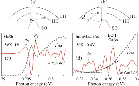
We confirm the hot-hole dynamics of Fig.4(a)for hetero-junctions. As photoexcited hot holes tend to relax to the top of the VB, an intervalence-band scattering typically occurs to enable the transfer of a hot hole between different bands [Fig. 4(b)], which is then followed by intraband hole-hole or hole-phonon scatterings for further relaxation, as reported
Photon energy (eV)
0.79 0.795 0.8
GaSb
5.6K, 1V
Δ0 ET
Yield
d2Yd(hν)2
Photon energy (eV)
0.32 0.34 0.36 0.38 0.4
In0.53Ga0.47As
Δ0 50K, -0.4V
LO(Γ)
GaAs
d2Yd(hν)2
Yield
HH HH
SO HH
HH
SO
(c) (d)
(b) (a)
FIG. 4. (Color online) (a) and (b) are schematics of hole transitions (vertical lines) and scattering processes (dashed lines), corresponding to the hot-relaxation pictures obtained in this study and reported by Ref.39, respectively. The energy bands plotted with solid and dashed-dotted lines are for the emitter and barrier, respectively. Spectral yield and second yield derivatives for (c)p-type GaSb/GaSb and (d)p-type InGaAs/InGaAsP/InP junctions.ET corresponds to
[image:5.608.313.560.105.156.2]transitions across the band gap of GaSb (Ref.20). The dashed straight line crossing with the yield spectrum is to show the location where the slope is about to change.
TABLE II. Comparison of 0 of GaAs, In0.53Ga0.47As, and
GaSb with reported values. The numbers in parentheses are uncertainties.
GaAs In0.53Ga0.47As GaSb
This work (meV) 339.2(0.3) 332.8(0.3) 794.8(0.03) Reported values (meV) 390–341a 329.6b 796c
aReferences26and27. bVurgaftmanet al.(Ref.26). cMu˜nozet al.(Ref.24).
in bulks.39 Hole-hole scatterings proceed in a fast time scale and dominate in the intraband (HH) relaxation. In the het-erojunction case, this leads to a higher-order relaxing process compared to Fig. 4(a), due to required additional scattering to facilitate the escape of a hot hole over a potential barrier. The relaxing picture of Fig.4(a)depicts relaxation towards to the SO top instead of the HH, correlating with observations that confirm phonon features associated with the HH→SO singularity. The potential barrier diverts the relaxation channel primarily through the SO band, which principally contributes to the yield outcome. Such a mechanism was also found in quantum-dot structures,40 where carriers in the wetting layer with low kinetic energy (near theŴpoint) are scattered into quantum dots.
The photoemission study was extended to inspect0 of GaSb (Ref. 20) and In0.53Ga0.47As, as shown in Figs. 4(c)
and 4(d), respectively. The values of 0 (Table II) are
obtained as 794.8±0.03 meV (GaSb) and 332.8±0.3 meV (In0.53Ga0.47As), which agree with the reported values of
796 meV (GaSb)24 and 329.6 meV (In0.53Ga0.47As).26 The
identified feature is also confirmed by observing an onset of the yield (a change in the slope). It is thus found that the second derivative peak at 365.4 meV for In0.53Ga0.47As [Fig.4(d)]
corresponds to the GaAs-like LO(Ŵ) phonon (32.6 meV), in agreement with the value of 33.3 meV reported by Adachi.41 The feature associated with the InAs-like phonon cannot be confirmed, probably due to much weaker coupling between the carrier and InAs-like phonon, compared to that between the carrier and GaAs-like phonon, as confirmed by optical reflection.42
In conclusion, we have directly measured valence-band spin-orbit splitting and determined phonons participating in IVB indirect transitions by using IPE spectroscopy. The VB splitting energy of GaAs was found to remain unchanged, although degenerate doping introduces appreciable band tail-ings. The major role of optical phonons in IVB processes is confirmed, providing experimental validation for evaluating free-carrier IVB absorption. IPE results also indicate the hot-hole dynamics in heterojunctions with dominant relaxation through intravalence-band scatterings.
This work was supported in part by the US Army Research Office under Grant No. W911NF-12-2-0035 monitored by William W. Clark, and in part by the US National Science Foundation under Grant No. ECCS-1232184. The University of Leeds acknowledges supports from the UK Engineering and Physical Sciences Research Council, and E.H.L. from the European Research Council Advanced Grant “TOSCA.”
[image:5.608.53.294.486.636.2]H.C.L. is thankful for support from the National Major Basic Research Projects (2011CB925603) and the Natural Science Foundation of China (91221201). H.C.L. supported this work in all aspects, including carrying out the device processing,
reading and commenting the manuscript, until his death in October 2013. The authors also acknowledge Vadym Apalkov and Ramesh Mani for reading the manuscript and for fruitful discussions.
*uperera@gsu.edu
†Present address: Physics of Energy Harvesting, CSIR-National
Physical Laboratory, New Delhi 110012, India.
1Z. Fei, A. S. Rodin, G. O. Andreev, W. Bao, A. S. McLeod,
M. Wagner, L. M. Zhang, Z. Zhao, M. Thiemens, G. Dominguez, M. M. Fogler, A. H. C. Neto, C. N. Lau, F. Keilmann, and D. N. Basov,Nature (London)487, 82 (2012).
2N. M. Gabor, J. C. W. Song, Q. Ma, N. L. Nair, T. Taychatanapat,
K. Watanabe, T. Taniguchi, L. S. Levitov, and P. Jarillo-Herrero,
Science334, 648 (2011).
3S. J. Moon, A. A. Schafgans, M. A. Tanatar, R. Prozorov, A.
Thaler, P. C. Canfield, A. S. Sefat, D. Mandrus, and D. N. Basov,
Phys. Rev. Lett.110, 097003 (2013).
4Z. Li, E. A. Henriksen, Z. Jiang, Z. Hao, M. C. Martin, P. Kim,
H. Stormer, and D. N. Basov,Nat. Phys.4, 532 (2008).
5T. Jungwirth, P. Horodysk´a, N. Tesaˇrov´a, P. Nˇemec, J. ˇSubrt,
P. Mal´y, P. Kuˇzel, C. Kadlec, J. Maˇsek, I. Nˇemec, M. Orlita, V. Nov´ak, K. Olejn´ık, Z. ˇSob´aˇn, P. Vaˇsek, P. Svoboda, and J. Sinova,
Phys. Rev. Lett.105, 227201 (2010).
6K. S. Burch, D. B. Shrekenhamer, E. J. Singley, J. Stephens, B. L.
Sheu, R. K. Kawakami, P. Schiffer, N. Samarth, D. D. Awschalom, and D. N. Basov,Phys. Rev. Lett.97, 087208 (2006).
7See, for example, R. Newman and W. W. Tyler,Phys. Rev.105, 885
(1957);R. Braunstein and L. Magid,ibid.111, 480 (1958).
8B. C. Chapler, R. C. Myers, S. Mack, A. Frenzel, B. C. Pursley,
K. S. Burch, E. J. Singley, A. M. Dattelbaum, N. Samarth, D. D. Awschalom, and D. N. Basov,Phys. Rev. B84, 081203 (2011).
9T. de Boer, A. Gamouras, S. March, V. Nov´ak, and K. C. Hall,
Phys. Rev. B85, 033202 (2012).
10M. Cardona, K. L. Shaklee, and F. H. Pollak,Phys. Rev.154, 696
(1967).
11Y. F. Lao, P. K. D. D. P. Pitigala, A. G. U. Perera, H. C. Liu,
M. Buchanan, Z. R. Wasilewski, K. K. Choi, and P. Wijewarnasuriya,Appl. Phys. Lett.97, 091104 (2010).
12For example, Ref.10reported various interband critical points at
different doping concentrations, except forE0andE0+0at the
Ŵpoint, at which doping-caused potential fluctuations perturb the band edge states.
13E. Kioupakis, P. Rinke, A. Schleife, F. Bechstedt, and C. G. Van de
Walle,Phys. Rev. B81, 241201 (2010).
14M. Takeshima,Phys. Rev. B32, 8066 (1985);A. Haug,Semicond.
Sci. Technol.5, 557 (1990).
15J. Batey and S. L. Wright,J. Appl. Phys.59, 200 (1986).
16J. Noffsinger, E. Kioupakis, C. G. Van de Walle, S. G. Louie, and
M. L. Cohen,Phys. Rev. Lett.108, 167402 (2012);A. Frova and P. Handler,ibid.14, 178 (1965).
17Y. F. Lao and A. G. Unil Perera,Phys. Rev. B86, 195315 (2012). 18R. J. Powell,J. Appl. Phys.41, 2424 (1970).
19N. Samarth,Nat. Mater.11, 360 (2012).
20See Supplemental Material at http://link.aps.org/supplemental/
10.1103/PhysRevB.88.201302 for information about sample structures, fabrication, and characterization. The photoemission study on GaSb is described.
21V. Afanas’ev,Internal Photoemission Spectroscopy: Principles and Applications(Elsevier, Amsterdam, 2010).
22K. Xu, C. Zeng, Q. Zhang, R. Yan, P. Ye, K. Wang, A. C. Seabaugh,
H. G. Xing, J. S. Suehle, C. A. Richter, D. J. Gundlach, and N. V. Nguyen,Nano Lett.13, 131 (2013);Y. Hikita, M. Nishikawa, T. Yajima, and H. Y. Hwang, Phys. Rev. B 79, 073101 (2009).
23T. B. Bahder,Phys. Rev. B41, 11992 (1990).
24M. Mu˜noz, K. Wei, F. H. Pollak, J. L. Freeouf, and G. W. Charache,
Phys. Rev. B60, 8105 (1999).
25P. Lautenschlager, M. Garriga, S. Logothetidis, and M. Cardona,
Phys. Rev. B35, 9174 (1987).
26A. G. Thompson, M. Cardona, K. L. Shaklee, and J. C. Woolley,
Phys. Rev.146, 601 (1966);I. Vurgaftman, J. R. Meyer, and L. R. Ram-Mohan,J. Appl. Phys.89, 5815 (2001).
27J. S. Blakemore,J. Appl. Phys.53, R123 (1982). 28E. O. Kane,J. Phys. Chem. Solids1, 82 (1956).
29M. Kuball, M. K. Kelly, M. Cardona, K. K¨ohler, and J. Wagner,
Phys. Rev. B49, 16569 (1994).
30Y. Zhang and S. Das Sarma,Phys. Rev. B72, 125303 (2005). 31D. Auvergne, J. Camassel, H. Mathieu, and M. Cardona,Phys. Rev.
B9, 5168 (1974).
32J. L. T. Waugh and G. Dolling,Phys. Rev.132, 2410 (1963). 33P. Giannozzi, S. de Gironcoli, P. Pavone, and S. Baroni,Phys. Rev.
B43, 7231 (1991).
34S. Steiger, M. Salmani-Jelodar, D. Areshkin, A. Paul, T. Kubis,
M. Povolotskyi, H.-H. Park, and G. Klimeck, Phys. Rev. B 84, 155204 (2011).
35The maximum operating temperature in our experiments is 250 K;
however, as a result of spectral noise, phonon features can only be resolved up to 140 K, at which the energy of LO phonon is only 0.2 meV less than that at 0 K. Such a small variation is within the uncertainty of measurements and thus not identifiable.
36B. Brill and M. Heiblum, Phys. Rev. B 49, 14762 (1994);
S. Hunsche, H. Heesel, A. Ewertz, H. Kurz, and J. H. Collet,ibid. 48, 17818 (1993).
37A. J. Kent, R. E. Strickland, K. R. Strickland, and M. Henini,
Phys. Rev. B54, 2019 (1996).
38M. Heiblum, D. Galbi, and M. Weckwerth,Phys. Rev. Lett.62, 1057
(1989);Q. O. Hu, E. S. Garlid, P. A. Crowell, and C. J. Palmstrøm,
Phys. Rev. B84, 085306 (2011);D. C. Tsui,Phys. Rev. Lett.21, 994 (1968).
39M. Woerner, T. Elsaesser, and W. Kaiser,Phys. Rev. B45, 8378
(1992).
40J. Wolters, M.-R. Dachner, E. Mali´c, M. Richter, U. Woggon, and
A. Knorr,Phys. Rev. B80, 245401 (2009).
41S. Adachi, P. Capper, S. Kasap, and A. Willoughby,Properties of Semiconductor Alloys: Group-IV, III-V and II-VI Semiconductors
(Wiley, Hoboken, NJ, 2009).
42M. Amiotti, G. Guizzetti, M. Patrini, A. Piaggi, A. Borghesi,