City, University of London Institutional Repository
Citation: Soudi, S. & Rahman, B. M. (2016). Design of a Compact Polarization Splitter by
Using Identical Coupled Silicon Nanowires. Journal of Lightwave Technology, 34(17), pp.
4169-4178. doi: 10.1109/JLT.2016.2577341
This is the accepted version of the paper.
This version of the publication may differ from the final published
version.
Permanent repository link: http://openaccess.city.ac.uk/16549/
Link to published version: http://dx.doi.org/10.1109/JLT.2016.2577341
Copyright and reuse: City Research Online aims to make research
outputs of City, University of London available to a wider audience.
Copyright and Moral Rights remain with the author(s) and/or copyright
holders. URLs from City Research Online may be freely distributed and
linked to.
City Research Online:
http://openaccess.city.ac.uk/
publications@city.ac.uk
Abstract ̶ ̵ Design of an ultra-compact polarization splitter (PS) based on silicon-on-insulator (SOI) platform is presented. The design incorporates two simply coupled identical silicon nanowires, which can be easily fabricated by using standard Complementary Metal-Oxide-Semiconductor (CMOS) technology and fully compatible with standard active silicon photonics platforms. It is shown here that a low-loss, 17.90 µm long compact PS, and wide bandwidth over the entire C-band can be achieved. Important waveguide design parameters such as the guide width, height and separation between them have been optimized, and modal birefringence and wavelength dependence have been calculated by using a full-vectorial H-Field finite element method. The optical power transfer characteristics have been calculated by using a rigorous least squares boundary residual method.
Index Terms—numerical analysis, finite element methods, nanophotonics, directional couplers, optical waveguides, silicon on insulator technology, polarization splitter.
I. INTRODUCTION
PTICAL systems incorporating rotationally symmetric optical fibers cannot maintain its polarization states as it encounters random bends, pressures, or manufacturing imperfections which allow power transfer between two orthogonally polarized modes. For many communication and sensing systems this creates a major problem where a specific polarization state is needed. In this case, a polarization independent or polarization diversity system would be useful.
Rather than pursuing difficult polarization-independent devices on SOI, alternatively a polarization diversity scheme could be employed [1]. TE/TM polarization splitters are important components for design and development of such polarization diversity optical systems, such as integrated-optic
gyroscopes, switches, modulators and polarization
independent receivers for coherent detection [2]. In this case, the orthogonal polarization components of the input light can first be split into two different waveguides by using a polarization splitter (PS). Following that, a polarization rotator (PR) [3] can be incorporated in one of the waveguides to rotate the polarization by 90°. Finally, for the rest of the optical system only one polarization needs to be processed. Therefore, on-chip optical polarization rotator and splitting are key functions for realizing polarization-transparent operation in photonic integrated circuits (PIC).
S. Soudi and B. M. A. Rahman are with the Department of Electrical and Electronic Engineering, City University, London EC 1V 0HB, U.K. (e-mail :
sasan.soudi.1@city.ac.uk, and B. M. A.Rahman@city.ac.uk
II. DESIGN OF POLARIZATION SPLITTERS
For the design of polarization splitter the polarization dependent modal properties are exploited. An optical waveguide with small index contrast the resulting modal birefringence is smaller. However, this modal birefringence increases for high index contrast waveguide such as silicon nanowires. On the other hand, use of anisotropic materials, such as Lithium Niobate [4], or ion-exchanged glass [5] or use of metal cladding [6] can enhance the modal birefringence. Several metals such as gold, silver, copper, and aluminum, have been used to generate large birefringence, which can effectively shorten the dimension of optical components. However, metal-clad waveguides are also inherently lossy. It has also been shown that instead of using metal cladding by using simple layered isotropic material, material birefringence can also be introduced [7]. This modal birefringence can be exploited in the design of guided-wave polarization splitter, by incorporating y-splitter, directional coupler, Mach-Zehnder interferometer (MZI) or multimode interference (MMI) based designs. The designs of asymmetrical y-splitter in highly anisotropic lithium niobate were reported by Masuda and Yip [4] and Wei and Wang [8]. However, as the angle for a y-splitter needs to be smaller than 1 degree to avoid excessive power loss, often the resulting devices are relatively long.
Among the viable designs, a popular approach is to exploit the polarization dependent coupling of directional coupler because of their simplicity and easy design and also reasonable performance. Modal birefringence of optical waveguides produces polarization dependent coupling length which can be exploited to design polarization splitter. Small material birefringence of GaAs was exploited to design a 3000
m long PS [9]. Metal clad can introduce strong modal
birefringence and Albrecht et al. reported a 1600 m long
metal clad InP rib waveguide based asymmetrical directional coupler [10] and later on Rajarajan et al. reported a more
compact 230 m PS [11]. On the other hand, silicon
waveguide can directly provide stronger shape birefringence
Kiyat et al. reported an even more compact 120m PS using
silicon rib waveguide [12].
Polarization splitters have also been designed by exploiting polarization dependent imaging distance of multimode MMI couplers. In an earlier work, simple modal birefringence was considered for an InP based design where the PS length was
1640 m [13] and later on a shorter 1023 m design was
reported [14]. For a very narrow width MMI, supporting only two modes, which is also known as zero-gap directional
Design of a compact polarization splitter by
using identical coupled silicon nanowires
S. Soudi, Member, IEEE, and B. M. A. Rahman, Fellow IEEE
MZI structures have also been considered for realizing PSs. In order to make a compact MZI a large birefringence is required. One of the earliest work, Soldano et al. reported [6]
a 3300m MZ based PS using metal clad in one arm. Liang et
al. [16] reported a 6000m long Mach-Zehnder design using
natural modal birefringence of silicon rib waveguide and more
recently Augustin et al. [17] reported a more compact 600m
long design using higher waveguide birefringence of silicon nanowires incorporating MMI sections in MZI.
Recently there have been extensive research activities to develop silicon based photonics, by exploiting well developed CMOS technology. This can allow incorporation of both photonic and electronic components on the same chip. The high index contrast of silicon waveguides also allows more compact waveguides, bends and also other functional devices. But its modal characteristics are also strongly polarization dependent due to the strong index contrast. The dependence of the TE and TM polarizations can be exploited to find the polarization splitting ratio in order to design a compact PS.
Apart from strip silicon nanowires [18], silicon-based slot waveguides [19], where a low refractive index slot region placed between two silicon nanowires with high refractive index have been intensively investigated due to their unique opportunities and many potential applications. It can be noted that slot waveguides are also strongly polarization-dependent.
Recently, PSs based on horizontal single [20] and multi-slotted waveguide structures [21] have also been proposed. On the other hand, using an asymmetrical DC with a silicon wire
and a vertical slot, a PS of 13.6 μm in length was
demonstrated experimentally [22]. Dai [23] and Fukuda et al. [24] have considered asymmetric directional coupler with a NW and slot waveguide, ignoring very long coupling length for TE mode compared to TM modes. Besides these,
polarization splitters incorporating hybrid plasmonic
waveguides [25], waveguide bend [26], arrayed waveguide grating (AWG) [27], liquid crystal [28], photonic crystal [29] and grating couplers [30] have also been reported.
The Si polarization splitter proposed here shows a very compact design. It does not use slot guide, which is more difficult to fabricate, nor uses metal clad, which introduces loss, but uses two simple straight nanowires. In this paper, design optimization of a Si polarization splitter based on mature SOI technology is presented which requires less complex fabrication process with single mask only and backed by a well-established semiconductor industry [31]. Another benefit could arise in this design, due to the use of identical coupled waveguides, which are generally expected to be less sensitive to the fabrication tolerances.
III. THEORY
Pure TM or TE mode can only exist in planar slab
waveguides (WGs) with one-dimensional confinement.
However, in all practical optical WGs with two-dimensional confinement, the modes can be classified as quasi-TM and quasi-TE modes, which contain all six components of the E and H fields. Besides that, in high index contrast silicon nanowires, the modal birefringence is much higher. To
a guided-wave device all the methods to be employed should be fully vectorial in nature. Accurate calculations of the modal solution for the fundamental quasi-TE and quasi-TM modes are of significant importance when designing a PS. In the design of a compact PS, a full vectorial method is needed to obtain modal solutions of the supermodes and vectorial modal field profiles of the constituent NW waveguides across the dielectric interface. Since, all the three components of the H-field components are continuous across the dielectric interfaces such a full-vectorial formulation used here, based on the minimization of the H-field based energy functional [32]:
* *
2
*
( ) -1( ) ( ) ( )
H H H H
H H
p dxdy
dxdy
(1)Where, H is the full-vectorial magnetic field, ω2 is the
eigenvalue where ω is the angular frequency of the wave,
* denotes a complex conjugate and transpose,and ε and µ are
the permittivity and permeability, respectively. The penalty term has also been included to reduce the appearance of spurious modes. In this paper, an in-house code incorporating these attractive features of this method is used to optimize the PS design. Although the FEM can be useful to calculate the propagation constants for the even and odd fundamental quasi-TE and quasi-TM supermodes and also their modal field
profiles, however, alone, this method cannot analyze
discontinuity along a guided-wave device. Although a full-vectorial beam propagation method (BPM) [33] can be used to calculate the power conversion between the two polarized modes, however, as the proposed structure being consists of only two discrete interfaces, a junction analysis method would be more efficient to use to find the excited modal coefficients at the junctions and to optimize the polarization splitter design. In this case, a powerful full-vectorial numerical approach, the Least Squares Boundary Residual (LSBR) method [34] has been used, which rigorously satisfies the continuity of the tangential magnetic and electric fields at the junction interface in a least squares sense. The LSBR approach looks for a stationary solution to satisfy the continuity conditions by minimizing the error energy functional, J, as given by [34], to satisfy the continuity conditions:
2 2 2
0
J EtI EIIt Z HtI HIIt d
(2)Where Z0 is the free-space impedance and α is the
dimensionless weighting factor to balance the electric and magnetic field components of the error functional J. In this
case, the integration is carried out at the junction interface, Ω,
between the straight NW and the coupled Si waveguides. The
LSBR method obtains the modal coefficients of the
transmitted and reflected modes at the junction. This approach would be rigorous yet computationally more efficient than the use of the BPM.
V. PRINCIPLE
without a metal clad section or a bent or a slot and composed of two NWs of equal height identified by H. This would be easy to fabricate by using the mature CMOS technology, incorporating two simple coupled identical nanowires.
For a directional coupler, its coupling length,
Lc= π/ (βe-βo), is the shortest length necessary for maximum
energy transfer, whereeandoare the propagation constants
of the even and odd supermodes of the coupled structure. For most of the practical waveguides the coupling length for the quasi-TE and quasi-TM modes are different but for low-index contrast waveguides the difference is small. As stated earlier, for a high index contrast this difference could be relatively larger and additionally by using anisotropic material, or metal clad the difference can be increased further. For highly birefringent NWs the coupling length for quasi-TE or TM
polarizations, LcTEand LcTMare significantly different and if
we can have L = m * LcTE = n * LcTM, where m and n are
integer and one of them is odd and other one even, then two orthogonally polarized waves will emerge from two different output ports, as shown in Fig.1. This condition may not be very difficult to achieve, but often yields larger m and n values. Performance error due to any fabrication tolerance is magnified by m or n, which often makes such design very sensitive to small changes in waveguide parameters. Here, our design target was to have m and n as small as possible, and for the best possible design to achieve m = 1 and n = 2. Hence, we
seek a design where, the coupling length for quasi-TE (LcTE)
polarization is twice that for the quasi-TM (LcTM) polarization,
if possible, allowing most of the quasi-TE and quasi-TM polarized powers to emerge from bar port and cross-port, respectively.
[image:4.612.369.507.383.489.2]L = m * LcTE= n * LcTM
Fig . 1. Principle of a polarization splitter. VI. RESULTS
The schematic cross-section of the coupled NWs is shown in Fig.2. Here, the width and height of the NW are shown by W and H, respectively and separation between the cores is shown as S. The refractive index of the Si and Silica are taken as 3.4754752 and 1.4440236, respectively, at the operating wavelength of 1.55 µ m.
Here the existing symmetry condition of the coupled structure has been exploited for the modal solutions of the directional coupler. This not only avoids mode degeneration by separating two interacting modes, but also would obtain more accurate solutions, with a given computer resources. Since this structure has one-fold symmetry, only half of the waveguide needs to be considered, which will allow a much
finer mesh division to be used. The combinations of n⨯H and
n.H at the vertical symmetry line have been used to find the
even and odd supermodes. From the modal solutions the coupling lengths for the quasi-TE and quasi-TM polarizations,
LcTE and LcTM, can be calculated and subsequently ratio of
these coupling lengths, RTE-TM( LcTE/ LcTM) is also calculated.
Like all other photonic devices, its performance will depend on the accuracy of the designs and also on the accuracy of the fabrication. However, design accuracy will also critically depend on the accuracy of the modal solutions. A small change of the separation distance (or its width and height) will not only change the quasi-TE and quasi-TM coupling lengths but also the RTE-TM, which will affect the performance and these are discussed in this paper.
The optical propagation in a directional coupler can be expressed in terms of the propagation constants of the even and odd supermodes of the coupled structures, or their
effective indices (neff = /k0, where k0 is the wavenumber
given by 2/), where neff (even) and neff (odd), and the
effective indices of the even and odd supermodes,
respectively. Accuracy of the Lc depends on the accuracy of
[image:4.612.51.277.426.519.2]the modal solutions, and more particularly on their differences, and it is critical that the accuracy of these parameters is established first. As most of the key design parameters are often obtained by using a given numerical method and it is also known that accuracy of these design parameters are also depend on the numerical parameters used, and as example, for the FEM the number of elements (or mesh divisions used) is the critical numerical parameter, and this is studied first.
Fig . 2. Cross-section of two identical coupled NWs.
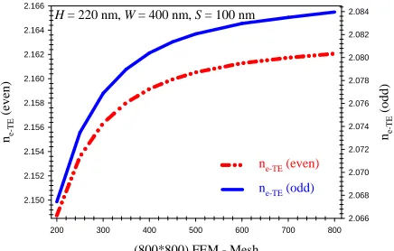
Variations of the effective indices, neffof the fundamental
quasi-TE (Hy11) even and odd supermodes for a silicon
nanowire with the mesh division are shown in Fig. 3. In this case, the waveguide Height (H), Width (W) and Separation (S), are taken as 220 nm, 400 nm, and 100 nm, respectively. For simplicity equal number of mesh division is used in both
the transverse directions. Variations of the ne-TE(even) and
ne-TE(odd) are shown by a blue solid line and a red dash-dotted
line, respectively. It can be observed that when the number of mesh increases, effective indices of both the fundamental quasi-TE supermodes increase. It can be noticed that, the effective index of TE even supermode is higher than that of the TE odd supermode (two different scales are used) and both reach their saturation points asymptotically. It should be noted
that when a 200 * 200 mesh is used neff is accurate up to 3rd
decimal place, and the accuracy is increased to 4th decimal
place when mesh size is increased to 800 * 800.
Variations of the effective indices of the quasi-TM (Hx11)
blue solid line and a red dash-dotted line, respectively. It can be observed here that as the mesh refinement is increased initially the effective index values increased, however, with a finer mesh rapidly converge to their saturation values. It should be noted that the range of effective index variation for the quasi-TM modes are relatively smaller than that of the quasi-TE modes shown in Fig.3.
H = 220 nm, W = 400 nm, S = 100 nm
(800*800) FEM - Mesh
200 300 400 500 600 700 800
n
e-T
E
(
ev
en
)
2.150 2.152 2.154 2.156 2.158 2.160 2.162 2.164 2.166
n
e-T
E
(
o
d
d
)
2.066 2.068 2.070 2.072 2.074 2.076 2.078 2.080 2.082 2.084
ne-TE (even)
ne-TE (odd)
Fig. 3. Variations of the effective indices of the quasi-TE even and odd supermodes with the mesh.
H = 220 nm, W = 400 nm, S = 100 nm
(800*800) FEM-Mesh Division
200 300 400 500 600 700 800
nef
f-T
M
(
ev
en
)
1.617 1.618 1.619 1.620 1.621 1.622 1.623
nef
f-T
M
(o
d
d
)
1.371 1.372 1.373 1.374 1.375 1.376 1.377
neff-TM (even)
neff-TM (odd)
Fig. 4. Variations of the effective indices of the quasi-TM even and odd supermodes with the mesh.
H = 220 nm, W = 400 nm, S = 100 nm
(800*800) FEM - Mesh Devision
0 200 400 600 800
Lc
T
E (
m
)
6 7 8 9 10 11
Lc
T
M (
m
)
3.14 3.16 3.18 3.20 3.22 3.24
LcTE (m)
LcTM (m)
Fig. 5. Variations of the coupling lengths for the quasi-TE and quasi-TM polarizations with the mesh.
From these modal solutions, coupling lengths of both
quasi-TE and quasi-TM polarizations, LcTE and LcTM, respectively,
can be calculated. Variations of the coupling lengths for the
fundamental quasi-TE and quasi-TM polarizations for
H = 220 nm, W = 400 nm and S = 100 nm with the mesh
polarizations, respectively. It can be observed from Fig. 5, that as the number of mesh is increased from 100 to 500, initially
the LcTE(solid) increases rapidly, but, with further increase in
the number of mesh, the LcTE reaches a stable values
asymptotically, but for the LcTMcurve (dash-dotted) decreases
exponentially as a number of mesh increases from 100 to 800, and reaches its stable value about 3.149 µm. Two separate
scales are used for LcTEand LcTM, and it should be noted that
changes in their values are rather small. It can also be
observed that LcTMvariation is more stable with the mesh, and
this is due to the fact that the fundamental quasi-TM (Hx11)
mode being close to its cut-off its variations with the
waveguide’s geometrical and numerical parameters is small.
Next, for the design of a polarization splitter the Lc ratio
(RTE-TM) is calculated from the polarized coupling lengths,
LcTE/ LcTM. Variation of this coupling length ratio (RTE-TM) for
H = 220 nm, W = 400 nm and S = 100 nm with the mesh
division is shown in Fig. 6. It can be noticed that as the number of the mesh division is increased, initially this ratio increases appreciably and then converges to its stable value. It
can be noted that Lcratio (RTE-TM) is accurate up to the second
decimal point when 800 * 800 mesh divisions are used. Following this all the numerical simulations are carried out using equivalent to or better than 800 * 800 mesh divisions in the two transverse directions, where more than 1.2 million first-order triangular elements have been employed to represent the half of the waveguide structures. In these cases, the horizontal and vertical mesh resolutions are better than 1 nm and 0.5 nm, respectively. We have bench-marked our mode solver code with the polarization splitter design reported
by Fukuda et al. [24]. We have obtained the LcTE and LcTM
values as 135.0m and 11.0m for the TE and
quasi-TM modes, respectively and Fukuda et al. reported their
device length between 1015m.
[image:5.612.52.270.164.303.2]Variations of the RTE-TM, with the waveguide width for three different heights, 260 nm, 280 nm and 300 nm, are shown in Fig. 7 by a solid blue line, a red dashed line and a black
dash-dotted line, respectively with the same
separation-S = 150 nm. It can be noticed that as the waveguide width
increases, the RTE-TM,also increases. It can be noted that it is
possible to obtain an ideal RTE-TM = 2.00, when quasi-TE and
quasi-TM modes can emerge from two different ports. However, care must be taken to make sure that the numerically simulated results are accurate. For H = 260 nm,
280 nm and 300 nm, when RTE-TM= 2.00 is achieved then the
corresponding waveguides widths would be 315 nm, 311 nm and 314 nm, respectively and for these three cases the device lengths would be equal to 4.940 µm, 5.235 µm and 6.180 µm, respectively. It can be noted that for H =260 nm, there is a
small discontinuity in the RTE-TMcurve, which was identified
as the point where Hx
11and Hy21modes are degenerate.
On the other hand, variations of the RTE-TM with the
waveguide height are shown in Fig. 8 by a blue solid line for
W = 315 nm, a dash-dotted red line for W = 314 nm and a
[image:5.612.52.271.340.477.2] [image:5.612.53.266.511.654.2]polarization. The non-monotonic changes of the Lc ratio has been identified to the modes approaching their cut-off conditions when the Height, H, was considerably lower. To
understand the non-monotonic nature of RTE-TMvariation as
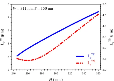
shown in Fig. 8, next, their individual coupling lengths are also presented. Variations of the coupling lengths as a function of the waveguide heights for the quasi-TE and quasi-TM polarizations are shown in Fig. 9 by a solid blue line and a red dashed dotted line, respectively. The quasi-TE and quasi-TM coupling lengths are shown by using two different scales. The coupling length for quasi-TE polarization presented by using
the left-hand Y–axis shows a usual near linear variation of the
coupling length. This is because, reduction in height increases evanescent field outside waveguide core, resulting stronger mode coupling and as a result, coupling length reduces. Variation of the quasi-TM coupling length is shown in Fig. 9 by using its right-hand Y-axis. Here, it can be observed that as
the waveguide height is reduced, initially Lc reduces slowly
with the height and then reaches a minimum value of 2.43 µm at H = 260 nm, then increases slightly as mode approaches its cut-off point (quasi-TM mode approaches cut-off earlier). This
non-monotonic variation of LcTM causes a similar
non-monotonic variation of their Lcratio, RTE-TM, as shown earlier
in Fig. 8. It can be observed from this figure that for a given width (say W = 315 nm) there can be two different waveguide heights which satisfy the design requirement of ratio, RTE-TM to be exactly 2.00. However, their performances, such as device lengths and more importantly the effects of fabrication tolerances could be different.
H = 220 nm, W = 400 nm, S = 100 nm
(800*800) FEM - Mesh Devision
0 200 400 600 800
RT
E
-T
M
(
Lc
T
E /
Lc
T
M)
1.8 2.0 2.2 2.4 2.6 2.8 3.0 3.2
Fig. 6. Variation of the coupling length ratio of the quasi-TE and quasi-TM supermodes with the mesh.
S = 150 nm
W (nm)
260 280 300 320 340 360 380
RT
E
-T
M
(
Lc
T
E / Lc
T
M )
1.0 1.5 2.0 2.5 3.0 3.5 4.0 4.5
H = 260 nm
H = 280 nm
[image:6.612.53.238.395.530.2]H = 300 nm
Fig. 7. Variations of the coupling length ratios of the quasi-TE and quasi-TM supermodes with the waveguide width for different heights.
Variations of the coupling lengths ratio, RTE-TM, with the waveguide separation for the quasi-TE and quasi-TM polarizations are shown in Fig. 10. The black short dashed, blue solid and long dashed red lines represent the H = 260 nm, 280 nm and 300 nm, with corresponding waveguide widths are 315 nm, 311 nm, and 314 nm, respectively. It can be observed from this figure that, as the separation between the waveguides is increased from 50 nm to 150 nm, the coupling
lengths ratio, RTE-TM increases. At higher separations, as the
guides are nearly isolated, the modal birefringence does not change any more with the waveguide separation. From Fig. 10, again a design relationship can be achieved such that
RTE-TM = 2.00. It can be noticed from this figure that for the
waveguide heights, H = 260 nm, 280 nm and 300 nm, the separation between the guides, S, should be 150 nm to get the
ideal value, RTE-TM = 2.00. In these cases, the polarization
splitter length should be equal to 4.940 m, 5.235 m and
6.180m, respectively.
Although the short device length can yield a compact polarizer, but it is also necessary to study their fabrication tolerances in order to understand their suitability for practical applications. Like all other photonic devices, its performance depends on the accuracy of fabrication. A small change in the width (or its height or their separation) would not only change their quasi-TE and quasi-TM polarization coupling lengths but
also change the Lc ratio (RTE-TM) from its desired value of
2.00. Performances of such PS against the fabrication tolerances related to its height, width and separation can be evaluated. A possible design was identified, when H = 280
nm, W = 311 nm, and S = 150 nm, resulting, LcTE= 5.235 µ m
and LcTM= 2.605 µm, giving RTE-TM=2.00. So, following an
accurate fabrication if the device length is equal to 5.235 µm, then, it is expected that quasi-TE mode will emerge from the Cross-port (Port 4) and quasi-TM mode in the Bar-port (Port 3).
At first, the variations of the quasi-TE power outputs in the Cross-port (P4-TE) and Bar-port (P3-TE) and quasi-TM outputs in the Cross-port (P4-TM) and Bar-port (P3-TM) as a function of separation between the waveguides are calculated, initially, by using a simple semi-analytical approach by considering their changes in the coupling lengths only. Later a more rigorous full-vectorial approach is used to find these values more accurately.
S = 150 nm
H ( nm )
220 240 260 280 300 320 340 360
RT
E
-T
M
(
Lc
T
E / Lc
T
M )
1.0 1.2 1.4 1.6 1.8 2.0 2.2
W = 315 nm W = 311 nm
W = 314 nm
Fig. 8. Variations of the coupling length Ratio, RTE-TM, with the waveguide
[image:6.612.314.506.557.698.2] [image:6.612.51.250.567.709.2]W = 311 nm, S = 150 nm
H ( nm )
240 260 280 300 320 340 360
Lc
T
E (
m
)
3 4 5 6 7
Lc
T
M
(
m
)
2.0 2.5 3.0 3.5 4.0 4.5
Lc TE
[image:7.612.52.251.56.198.2]Lc TM
Fig. 9. Variations of the coupling lengths with the waveguides heights.
Figure 11 shows the variations of the power transfer as a function of the separation between the waveguides, when
H = 280 nm and W = 311 nm, and the device length is kept
fixed at L = 5.235 µ m, as designed. As can be observed from this figure, when, S = 150 nm, as planned, at device length is
equal to L = LcTE≈ 2 * L
cTM= 5.235 µm, for both quasi-TM
polarization for quasi-TE polarization, most of the power will emerge from the Bar-port (P3-TM) and in the Cross-port (P4-TE), shown by red dashed-dotted and blue solid lines, respectively. Also, the black dashed-dotted and the green dashed lines show the quasi-TE power transfer characteristics in Port 3 (P3-TE) and the quasi-TM power transfer characteristics in port 4 (P4-TM), respectively. As can be seen from the figure, at the end of the coupling length, for both quasi-TM and quasi-TE polarized modes, almost zero power remained in Bar-port (P4-TM) and Cross-port (P3-TE). Therefore, by careful selection of the device parameters, a desired design for the polarization splitter is obtained. It can be noticed from these curves that a small change in waveguide separation can deteriorate the device performances. This phenomenon can be explained with the help of Fig. 10. It can be noticed that as the waveguides separation is deviated from the design value of the RTE-TM value of 2.00, not only the ratio will increases, but also the resulting coupling length would not match with the device
length and hence deteriorate of the power transfer
characteristics. This also shows power output for the quasi-TM mode is more sensitive compare to the quasi-TE polarization power mode, as here n being twice of m, the phase error for quasi-TM mode mismatch would be double that of the quasi-TE mode.
S ( nm )
40 60 80 100 120 140 160 180 200 220
RT
E
-T
M
(L
c
T
E / Lc
T
M )
1.5 1.6 1.7 1.8 1.9 2.0 2.1
H = 260 nm, W = 315 nm H = 280 nm, W = 311 nm
H = 300 nm, W = 314 nm
Fig. 10. Variations of the coupling length Ratio, RTE-TM, with the waveguide
separation, S.
coefficients of the supermodes excited at the start of the directional coupler. To satisfy the continuity of the tangential
electric and magnetic fields, Etand Ht, an incident mode not
only generates two supermodes but may also excite other higher-order guided or radiating modes. In this study a rigorous full-vectorial least squares boundary residual method [34] is used to find the modal coefficients of the two
supermodes. From the modal coefficients, their propagation
constants and full vectorial modal field profiles the evolution of quasi-TE and quasi-TM power along the waveguide branches can be calculated more rigorously. Variations of the TE and TM power in Port 4 and Port 3, with the propagation distance are shown in Fig.12. It can be observed that at Z = 0, 96% of the input TE power is coupled to Port 3 as shown by a solid blue line and this value reduces along the propagation
distance. At a distance Z = L = LcTE, most of this power has
been transferred to Port 4, shown by a red dashed-dotted line. Similarly, at Z = 0, nearly 81% of the input TM power was coupled to Port 3, as shown by a green dashed-dotted line,
however, at a distance Z = L = 2 * LcTM, most of this returns to
Port 3, since this distance is double of its coupling length. On the other hand, TM power in port 4, shown but a black dashed
line, shows its maximum value at Z = L / 2 = LcTM.
Any deviation from the ideal design will not only change the coupling lengths, and their ratio, but also the modal coefficients of the excited modes in the directional coupler section. From the modal coefficients, their propagation constants and full vectorial modal field profiles the evolution of quasi-TE and quasi-TM power along the waveguide branches can be calculated more rigorously. Figure 13 shows the variation of the power transfer for different separations between the waveguides for H = 280 nm and W = 311 nm. The
red dashed-dotted line P4-TE (LSBR) and the dark green
dashed-dotted-dotted line P3-TM (LSBR) show the power
transfer characteristics for the quasi-TE and polarized modes in the Cross-port (Port 4) and quasi-TM mode in the Bar-port (Port 3), respectively. From the rigorous LSBR method, the
transmitted coefficients Ce
yand Coyfor the quasi-TE even and
odd supermodes are obtained as 0.83536 and 0.67721, respectively, when S = 150 nm. In this case, for the quasi-TE mode power transfer to Cross-Port (P4-TE) was 92 %, represent only 0.40 dB loss. The transmitted coefficients of the even and odd quasi-TM supermodes are obtained as 0.81770 and 0.58613, respectively, and 77 % power transferred to Bar-Port (P3-TM) with a loss value of 1.10 dB. For references, the results by using simple analytical approach, only considering the changes in the coupling length are shown again in Fig. 13 by solid blue and black dashed lines. In this case, it can be noticed that transfer of quasi-TM mode in Port 3 has deteriorated significantly compared to the power transfer of quasi-TE mode in Port 4. It should be noted that for such typical nanowires, as often height is smaller than its width, the
effective index of the fundamental quasi-TM (Hx11) mode is
much lower than that of the fundamental quasi-TE (Hy11)
[image:7.612.53.240.579.722.2]incomplete cancellation of modal fields in the two waveguides, and similarly in this case power loss for the quasi-TM polarization has been higher.
H = 280 nm W = 311 nm
S (nm)
80 100 120 140 160 180 200 220 240 260 280
P
o
we
r
co
u
p
li
n
g
e
ff
ic
ie
n
cy
0.0 0.2 0.4 0.6 0.8 1.0
P3-TM P3-TE
P4-TM P4-TE FEM
Fig. 11. Variations of the power coupling efficiency with the separation.
H = 280 nm, W = 311 nm S = 150 nm, L = 5.24m
Z (m)
0 1 2 3 4 5
P
o
w
er
T
ra
n
sf
er
0.0 0.2 0.4 0.6 0.8 1.0
P3-TM
P3-TE
P4-TM P4-TE
Fig. 12. Variations of the quasi-TE and quasi-TM powers in Ports 4 and 3 along the axial direction.
S (nm)
100 120 140 160 180 200 220 240 260
P
o
w
er
c
o
u
p
li
n
g
e
ff
ic
ie
n
cy
0.0 0.2 0.4 0.6 0.8 1.0
P3-TM (FEM)
P4-TE (FEM)
P3-TM (LSBR) P4-TE (LSBR)
H = 280 nm W = 311 nm
Fig. 13. Variations of the power coupling efficiency with the changes in the separation, S.
Therefore, it is expected that by reducing the coupling for both quasi-TE and quasi-TM polarized modes, it may be possible to reduce the power loss for both the polarizations. However, coupling lengths for both the TE and quasi-TM modes will increase which will make the device length a
bit longer. Besides that Lcratio will also change, however, it
is still possible to achieve the desired Lcratio (RTE-TM) of 2.00
by adjusting other waveguide parameters, such as, its width and height. Figure 14 shows the variation of the power transfer
for the quasi-TE and quasi-TM polarized modes as a function of the waveguide separation by using the LSBR method. In this case, its height was kept fixed at 300 nm, and width was
adjusted to achieve RTE-TM= 2.00 for a given separation. It can
be noticed that, by increasing the separation between the waveguides width, transferred power of quasi-TE polarized mode to the Port - 4 and quasi-TM polarized mode into the Port - 3 are increased. It can be noticed from this figure that when the separation between the guides change from the 140 nm to the 300 nm, the power transfer increased from the 0.9415 to 0.9543 for the quasi-TE input in Port-4 and from 0.8055 to 0.8429 for the quasi-TM polarized modes in Port-3, respectively. At the same time, the cross-talk improved from -18.6 dB to -26 dB for the quasi-TE input and from -13 dB to the -20 dB for the quasi-TM polarized modes, respectively (but not shown here). The black dashed-dotted curve in Fig. 14 shows the coupling length for the quasi-TE mode (the
right-hand Y –axis scale) as a function of the waveguide
separation. It can be seen from this figure that, as the separation between the guides is increased from 140 to 300
nm, the coupling length (L = Lcy) increases linearly from 5.0
µ m to 17.9 µm.
Weak coupling can also make the device sensitive with the fabrication tolerances. Therefore, it may be necessary to control the separation of these waveguides within a few nanometers, and sensitivity of this parameters, must be studied. Variation of the power transfer for the different separation between the waveguides for H = 300 nm, W = 317 nm and L = 17.9 µm are studied next, and shown in Fig. 15.
The solid blue shows the quasi-TE power transfer
characteristics in Port 4 (P4-TE) by using the LSBR result. The dashed red line shows that the quasi-TM power transfer
characteristics in Port 3 (P3-TM). In this case most of the
quasi-TE polarized power transferred to Cross-Port (P4-TE) with only 0.21 dB loss and quasi-TM power into Bar-Port (P3-TM) with 0.74 dB loss. It can be noticed that from this curve that the deterioration of the quasi-TM power transfer characteristics (P3-TM) is more severe than the quasi-TE case. It can be noted that quasi-TE output power in Cross-Port is better than 50 % of its maximum value, when separation is in the range of 240 nm to 400 nm. On the other hand quasi-TM output in the Bar-Port is better than 50 % of its maximum value, when separation is between 275 nm to 340 nm. This narrower quasi-TM range is due to n being double of m. In Fig. 15, the green dashed-dotted line shows the cross-talk in the Bar-port (P3-TE) for the quasi-TE case and the dashed-dotted black line shows the cross-talk in the Cross-port (P4-TM), for the quasi-TM polarization mode, calculated by the LSBR method. It can be noticed that change in separation can deteriorate the cross-talk for the both cases, but this also shows cross-talk for quasi-TM mode is more sensitive compare to the quasi-TE mode. As can be seen from this figure, when S = 300 nm, at the end of the device length, for both the quasi-TE and quasi-TM modes, almost zero power remained in Port 3 and Port 4, respectively. Effects of width and height variations were also studied but not shown here. It
can be noted that when its height changed by 20 nm from
the design value of 280 nm, the quasi-TE power transfer was better than 80% of its maximum value. Similarly when the
[image:8.612.49.248.97.240.2] [image:8.612.51.251.270.420.2] [image:8.612.53.255.454.603.2]TM mode was more sensitive and its height and width changes
need to be within 10 nm for the same 80% power transfer
limit.
This structure has been optimized for the operating
wavelength of = 1550 nm. Any changes in the operating
wavelength will change the coupling length, coupling length ratio and also the supermode coefficients. Figure 16 illustrates the power transfer as a function of the operating wavelength. This figure shows the coupled power in the bar and cross ports for the quasi-TE and quasi-TM polarizations, respectively.
H = 300 nm
S ( nm )
140 160 180 200 220 240 260 280 300
P
o
w
er
c
o
u
p
li
n
g
e
ff
ic
ie
n
cy
0.80 0.82 0.84 0.86 0.88 0.90 0.92 0.94 0.96
Lc
T
E (
m
)
4 6 8 10 12 14 16 18 20
P3-TM
P4-TE
LcTE (m)
[image:9.612.53.265.200.343.2]LSBR
Fig.14. Variation of the power transfer for the quasi-TM and quasi-TE modes, and coupling length of the quasi-TE mode with the waveguide separations, S.
H = 300 nm, W = 317 nm
S (nm)
220 240 260 280 300 320 340 360 380 400 420
P
o
w
er
c
o
u
p
li
n
g
e
ff
ic
ie
n
cy
0.0 0.2 0.4 0.6 0.8 1.0
P3-TM
P3-TE
P4-TM
[image:9.612.316.519.228.380.2]P4-TE LSBR
Fig.15. Variation of the power transfer for the different separations between the waveguides, for H = 300 nm and W = 317 nm.
Since there is a weaker coupling for quasi-TE polarization compare to quasi-TM polarization, the response for quasi-TE polarization is broadband. Figure 16 shows that, the crosstalk in the Cross-port smaller for quasi-TE mode than that in the Bar-port for quasi-TM mode, because the confinement of the quasi-TE mode is stronger than the quasi-TM mode. It can be noticed from these curves that as the wavelength changes, power transfer characteristics also changes and this will also change the phase matching conditions. However, it is shown here that, the effect of small change in the wavelength is quite small. This indicates that for many practical applications the device will have a larger operating bandwidth. The effect of temperature variation has also been studied for this device but this is not presented here. It was identified that a small amount of temperature tuning may be possible, which can be used to
amount of wavelength tuning can also be used to compensate the fabrication tolerances.
VII. CONCLUSION
The design presented in this work uses two identical silicon nanowires, which would be simpler than the design approaches reported earlier by using slot waveguides [20-23]. As the proposed structure does not consider any bent section or slanted side wall [18], and [31], or trench with different etch depth [12, 17, 31] so, it would be easier to fabricate. No metal clad has been used which avoids plasmonic modal loss.
H = 300 nm, W = 317 nm S = 300 nm
Wavelength (nm)
1440 1460 1480 1500 1520 1540 1560 1580 1600 1620
P
o
w
er
c
o
u
p
li
n
g
e
ff
ic
ie
n
cy
0.0 0.2 0.4 0.6 0.8 1.0
P3-x
P3-y
P4-x
P4-y
LSBR
Fig. 16.Variation of the power transfer with the wavelength for H = 300 nm, S = 150 nm and W = 317 nm.
[image:9.612.52.249.387.536.2]VIII. REFERENCES
[1] T. Barwicz, M. R. Watts, M. A. Popović, P. T. Rakich, L. Socci, F. X. Kärtner, E. P. Ippen, and H. I. Smith, “Polarization-transparent
microphotonic devices in the strong confinement limit,”Nat. Photonics
1 , pp. 57–60 , Dec. 2007.
[2] B. Glance, “Polarization independent coherent optical receivers,”
J. Lightw. Technol., vol. 5, no. 2, pp. 274–276, Feb. 1987.
[3] S. Soudi, and B. M. A. Rahman, “Design of compact polarization rotator using simple silicon nanowires,”Appl. Opt. vol. 53, no. 34, pp. 8071-8077, Dec. 2014.
[4] M. Masuda, and G. L. Yip, “An optical TE-TM mode splitter using a LiNbO3branching waveguide,”Appl. Phys. Lett., vol. 37, no.1, pp.
20-22, Jul. 1980.
[5] A. N. Miliou, R. Srivastava, and R. V. Ramaswamy, “A 1.3-µm directional coupler polarization splitter by ion exchange,” J. Lightw. Technol., vol. 11, no. 2, pp. 220–225, Feb. 1993.
[6] L. B. Soldano, A. H. de Vreede, M. K. Smit, B. H. Verbeek, E. G. Metaal, and F. H. Groen, “Mach-Zehnder Interferometer polarization splitter in InGaAsP/InP,”IEEE Photon. Technol. Lett., vol. 6, no. 3, pp. 402-405, Mar. 1994.
[7] M. Rajarajan, andB. M. A. Rahman, and K. T. V. Grattan, “A novel and
compact optical polarizer incorporating a layered waveguide core
structure,” J. Lightw. Technol., vol. 21, no. 12, pp. 3463–3470, Dec. 2003.
[8] P. Wei, and W. Wan., “A TE-TM mode splitter on lithium niobate using
Ti, Ni, and MgO diffusions,”IEEE Photon. Technol. Lett., vol. 6, no. 2, pp. 245-248, Feb. 1994.
[9] F. Ghirardi, J. Brandon, M. Carre, A. Bruno, L. Menigaux, and A. Carenco, “Polarization splitter based on modal birefringence in InP/InGaAsP optical waveguides,”IEEE Photon. Technol. Lett., vol. 5, no. 9, pp. 1047-1049, Sep. 1993.
[10] P. Albrecht, M. Hamacher, H. Heidrich, D. Hoffman, H. P. Nolting, and
C. M. Weinert., “TE/TM mode splitters on InGaAsP/InP,”IEEE Photon. Technol. Lett., vol. 2, no. 2, pp. 114-115, Feb. 1990.
[11] M. Rajarajan, C. Themistos, B. M. A. Rahman, and K. T. V. Gratan,
“Characterization of metal-clad TE/TM mode splitters using the finite
element method,”J. Lightw. Technol., vol. 15, no. 12, pp. 2264-2269, Dec. 1997.
[12] I. Kiyat, A. Aydinli, and N. Dagli, “A compact silicon-on-insulator
polarization splitter,”IEEE Photon. Technol. Lett., vol. 17, no. 1, pp. 100–102, Jan. 2005.
[13] B. M. A. Rahman, N. Somasiri, C. Themistos, and K. T. V. Grattan,
“Design of optical polarization splitter in a single-section deeply etched
MMI waveguides,”Appl. Phys. Lett. vol. 73, no. 5, pp. 613-618, Oct. 2001.
[14] J. M. Hong, H. H. Ryu, S. R. Park, J. W. Jeong, S. G. Lee, E. Lee, S. Park, D. Woo, S. Kim, and O. Beom-Hoan, “Design and fabrication of a
significantly shortened multimode interference coupler for polarization splitter application,”IEEE Photon. Technol. Lett., vol. 15, no. 1, pp. 72-74, Jan. 2003.
[15] B. K. Yang, S. Y. Shin, and D. Zhang, “Ultrashort polarization splitter
using two-mode interference in silicon photonic wires,”IEEE Photon. Technol. Lett., vol. 21, no. 7, pp. 432-434, Apr. 2009.
[16] T. K. Liang and H. K. Tsang., “Integrated polarization beam splitter in
high index contrast silicon-on-insulator waveguides,” IEEE Photon. Technol. Lett., vol. 17, no. 2, pp. 393-395, Feb. 2005.
[17] L. M. Augustin, R. Hanfoug, J. J. G. M. van der Tol, W. J. M. de Laat,
and M. K. Smit,“ A compact integrated polarization splitter/converter in InGaAsP-InP,”IEEE Photon. Technol. Lett., vol. 19, no. 17, pp. 1286-1288, Sep. 2007.
[18] D. Dai, Y. Shi, and S. He, “Characteristic analysis of nanosilicon rectangular waveguide for planar light-wave circuits of high integration,”Appl. Opt. vol. 45, no. 20, pp. 4941-4946, Jul. 2006. [19] V. R. Almeida, Q. Xu,C. A. Barrios, and M. Lipson, “Guiding and
confining light in void nanostructure,”Opt. Lett., vol. 29, no. 11, pp. 1209-1211, Jun. 2004.
[20] Y. Fei, S. Chen, L. Zhang, and T. Cao, “Design and analysis of polarization splitter based on a horizontal slotted waveguide,”Opt. Eng., vol. 51, no. 5, pp. (054601-1)-(054601-4), May 2012.
[21] J. Xiao, X. Liu, and X. Sun, “Design of a compact polarization splitter in horizontal multiple-slotted structure,”J. Appl. Phys., vol. 47, no. 5, pp. 3748–3754, May 2008.
[22] S. Lin, J. Hu, and K. B. Crozier, “Ultracompact broadband slot
waveguide polarization splitter,”Appl. Phys. Lett., vol. 98, no. 15, pp. (151101-1)-(151101-3), Apr. 2011.
[23] D. Dai, Z. Wang, and J. E. Bowers, “Ultrashort broadband polarization beam splitter based on an asymmetrical directional coupler,”Opt. Lett., vol. 36, no. 13, pp. 2590-2592, Jul. 2011.
[24] H. Fukuda, K. Yamada, T. Tsuchizawa, T. Watanabe, H. Shinojima, and
S. Itabashi, “Ultrasmall polarization splitter based on silicon wire waveguides, Opt. Express, vol. 14, no. 25, pp. 12401-12408, Dec. 2006. [25] X. Guan, H. Wu, Y. Shi, and D. Dai, “Extremely small polarization
beam splitter based on a multimode interference coupler with a silicon
hybrid plasmonic waveguide,” Opt. Lett., 39, no. 2, pp.259-262, 2014. [26] C. Van Dam, L. H. Spiekman, F. P. G. M. van Ham, F. H. Groen, J. J. G.
M. van der Tol, I. Moerman, W. W. Pascher, M. Hamacher, H. Heidrich,
C. M. Weinert, and M. K. Smit, “Novel compact polarization converters
based on ultra short bends,”IEEE Photon. Technol. Lett., vol. 8, no. 10, pp. 1346-1348, Oct. 1996.
[27] W. N. Ye, D. X. Xu, S. Janz, P. Waldron, P. Cheben, and N. G. Tarr,
“Passive broadband silicon-on-insulator polarization splitter,”Opt. Lett., vol. 32, no. 11, pp. 1492–1494, May 2007.
[28] Q. Wang, G. Farrell, and Y. Semenova, “Design of integrated polarization beam splitter with liquid crystal,” IEEE J. Sel. Topics Quantum Electron., vol. 12, no. 6, pp. 1349–1353, Nov. 2006.
[29] Y. Shi, D. Dai, and S. He, “Proposal for an ultracompact polarization-beam splitter based on a photonic-crystal-assisted multimode interference coupler,”IEEE Photon. Technol. Lett., vol. 19, no. 11, pp. 825-827, Jun. 2007.
[30] Y. Zhang, Y. He, J. Wu, X. Jiang, R. Liu, C. Qiu, X. Jiang, J. Yang, C. Tremblay, and Y. Su, “High-extinction-ratio silicon polarization beam splitter with tolerance to waveguide width and coupling length
variations,” Optics Express, 24, pp.6586-6593, Mar. 2016.
[31] D. Dai, L. Liu, S. Gao, D. Xu, and S. He, “Polarization management for
silicon photonic integrated circuits,”Laser Photon. Rev., vol. 7, no. 3, pp. 303-328, may 2013.
[32] B. M. A. Rahman, and J. B. Davies, “Finite element solution of integrated optical waveguides,”J. Lightw. Technol., vol. LT-2, no. 5, pp. 682-688, Oct. 1984.
[33] S. S. A. Obayya, B. M. A. Rahman, and H. A. El-Mikati,“New full -vectrorial numerically efficient propagation algorithm based on the finite
element method,”J. Lightw. Technol., vol. 18, no. 3, pp. 409-415, Mar. 2000.
[34] B. M. A. Rahman and, J. B. Davies, “Analysis of optical waveguide discontinuities,ˮJ. Lightw. Technol. vol. 6, no.1, pp. 52-57, Jan. 1998.
IX. BIOGRAPHIES
B. M. Azizur Rahmanreceived BSc Eng. and MSc Eng. degrees in Electrical Engineering with distinctions from Bangladesh University of Engineering and Technology (BUET), Dhaka, Bangladesh, in 1976 and 1979, respectively. He also received two gold medals for being the best undergraduate and graduate student of the University in 1976 and 1979, respectively. He received his PhD degree in Electronic Engineering from University College, London in 1982. From 1976 to 1979, he was a Lecturer at the Electrical Engineering Department, BUET. After completing his PhD he joined University College London as a Post-doctoral Research Fellow and continued his research work on the finite element modeling of optical waveguide until 1988. In 1988, he joined the Electrical, Electronic and Information Engineering Department of City University, London, as a Lecturer, where he is now a Professor. Prof. Rahman has published more than 500 journal and conference papers and his journal papers have been cited more than 3300 times. Prof. Rahman is a Fellow of the Institute of Electrical and Electronic Engineers (IEEE) in USA, Optical Society of America (OSA), and the Society of Photo-optical Instrumentation Engineers (SPIE).
S. Soudi received the BSc Eng. degree in Electronics, and MSc Eng. degree in