Theses
8-13-2019
A Study on Copper-Gate Integration with
Titanium Interface Layers for IGZO TFTs
Harithshanmaa Sethupathi
[email protected]Follow this and additional works at:https://scholarworks.rit.edu/theses
This Thesis is brought to you for free and open access by RIT Scholar Works. It has been accepted for inclusion in Theses by an authorized administrator of RIT Scholar Works. For more information, please [email protected].
Recommended Citation
Harithshanmaa Sethupathi August 13, 2019
A Thesis Submitted in Partial Fulfillment
of the Requirements for the Degree of Master of Science
in
Microelectronic Engineering
Harithshanmaa Sethupathi
Committee Approval:
Dr. Karl HirschmanAdvisor Date
Professor
Dr. Dale Ewbank Date
Senior Lecturer
Dr. Ivan Puchades Date
Assistant Professor
Certified By:
Dr. Karl HirschmanAdvisor Date
Professor
Dr. Robert Pearson Date
Microelectronic Engineering Program Director
To the greatest teachers of my life- from walking, to talking and advice in making
life’s biggest decisions, for giving me the freedom and for encouraging me, Thank you
amma and appa. You will always be my heroes.
I would not have been able to do this without Dr.Karl Hirschman, a fatherly figure
away from home.He was there to always make me feel like home, who supported me
and guided me throughout both professionally and personally. I’m forever grateful
for what you have given me. Thank you Dr.Hirschman. You will always be my go to
person.
Dr.Robert Pearson- I wouldn’t have been able to do what I wanted to without you.
You welcomed me into the department and made it possible for me to learn what I
have wanted to for years. Thank you.
Dr.Fuller-My inspiration to get into this department. Having had the opportunity to
be in his class was a blessing. I Will always be a proud RIT Microelectronics graduate
because of Dr.Fuller. Thank you.
I would like to thank all the technicians at SMFL, Bruce, Rich, John and Patricia
and Sean for not giving up on us and helping us in the cleanroom. Working in the
cleanroom wouldn’t have been fun if it wasn’t for any of them. They were a great
support to me.
I would like to thank Team Eagle for supporting the work and me throughout. It
was a wonderful three years of grad school.I would especially like to thank Glenn and
Kabir for their constant support and motivation.
I would like to thank my friends Pratheik, Lilian, Patty, Udita and Viraj and Sanjna
for always pushing me to do better and making learning fun. My friends Divya,
Mythili, Arun, Sandesh, Abhilash for constantly being by my side and never giving
up on me.
The continuous demand for ultra-high resolution and improved video performance
on increasingly larger active-matrix displays has advanced the research field of thin
film transistors (TFTs) materials, processes and devices. Performance improvements
demonstrated by amorphous Indium-Gallium-Zinc-Oxide (IGZO) TFTs has enabled
a commercialized backplane technology adopted for AM-OLED displays, providing
advantages in device performance and uniformity at a much lower cost than Low
Temperature Poly-crystalline Silicon (LTPS). However as the display size gets larger
and the pixel density increases, charge transfer from the column driver to the pixel
through the addressed row TFT within the required time interval becomes
increas-ingly difficult. As the pixel size shrinks and the panel size grows, interconnects that
must be scaled down in cross-section have to transport charge over longer distances.
In addition, as the numbers of rows increase in a display, the time allowed for charge
transfer decreases to maintain a high image refresh frequency. These challenges must
be addressed by lower interconnect delay, thus the advantage in transitioning to Cu for
long interconnect rows and columns. The gate electrodes are usually implemented as
an appendage of the row interconnect, thus Cu-gate TFTs would avoid added process
complexity while supporting high-speed interconnects and low production costs. The
following work presents a study on Cu-gate integration and potential channel
contam-ination on bottom-gate IGZO TFTs with a newly established baseline process. Cu
was used in place of Mo as the gate electrode, with an underlying Ti layer to promote
adhesion to the oxidized silicon substrate. The experimental design input factors
included the option of a Ti capping layer on the Cu-gate, and the anneal conditions
of the gate dielectric (PECVD SiO2) prior to IGZO sputtering. Distinct differences
in physical and electrical responses over all treatment combinations were identified.
Experimental results demonstrated that while the Ti capping layer promoted
oxide without the use of Ti capping layer, as well as reduce oxide charge levels.
Cop-per contamination did not appear to be an issue in treatment conditions at or below
400oC, however pitting of the gate electrode occurred at anneal temperature above
400oC, as well as electrical results that suggest evidence of Cu contamination. Visual
observations and electrical characteristics are presented with a detailed discussion on
comparisons between treatment combinations, with reference to the baseline IGZO
Signature Sheet i
Abstract iv
Table of Contents vi
List of Figures viii
List of Tables xi
List of Symbols xii
1 INTRODUCTION 1
1.1 OVERVIEW . . . 1
1.2 RECENT DEVELOPMENT IN BACKPLANE TECHNOLOGY . . . 4
1.3 STRUCTURE OF DISPLAY DEVICES . . . 5
1.3.1 LIQUID CRYSTAL DISPLAY . . . 5
1.3.2 THIN FILM TRANSISTOR . . . 7
1.3.3 AM-OLED DISPLAY . . . 8
1.4 MOTIVATION OF STUDY . . . 10
1.5 GOALS AND OBJECTIVES . . . 13
1.6 DOCUMENT OUTLINE . . . 13
2 ELECTRONIC AND MATERIAL PROPERTIES OF IGZO 15 2.1 MATERIAL PROPERTIES OF IGZO . . . 15
2.2 CONDUCTION MECHANISM IN IGZO . . . 20
2.3 DENSITY OF STATES . . . 21
2.4 IGZO TFT CHARACTERISTICS . . . 23
2.5 MATERIAL MODELLING FOR TCAD SIMULATION . . . 24
3 IGZO TFT PROCESS DEFINITION AND BASELINE PROCESS MODIFICATION 27 3.1 TFT FABRICATION . . . 28
3.1.1 DIFFERENT ELECTRODE CONFIGURATION . . . 29
3.3 DESIGN OF EXPERIMENTS ON FABRICATION OF TFTs . . . . 35
3.3.1 IGZO THICKNESS AND BACKCHANNEL INTERFACE . . 36
3.4 PASSIVATION AND ANNEAL CONDITIONS . . . 38
3.4.1 MODIFIED FABRICATION PROCESS FLOW . . . 40
3.5 THERMAL INSTABILITY OF IGZO TFTs . . . 41
3.5.1 THERMAL STRESS RESPONSE ON MODIFIED BASELINE PROCESS . . . 43
3.6 SUMMARY . . . 45
4 INTEGRATION OF COPPER AS THE BOTTOM GATE ELEC-TRODE 47 4.1 CHALLENGES OF COPPER INTEGRATION . . . 48
4.1.1 PROCESS INTEGRATION . . . 49
4.1.2 DEVICE FABRICATION . . . 51
4.2 RESULTS . . . 52
4.2.1 MATERIAL DELAMINATION AND PITTING DEFECTS . 52 4.2.2 ELECTRICAL CHARACTERISTICS . . . 56
4.3 SUMMARY . . . 59
5 CONCLUSION 61
1.1 Comparison of IV characteristics of TFTs with different active channel
materials [1] . . . 2 1.2 FPD manufacturers are adding significant production capacity for Gen10+
FPDs, represented by the orange bar segments. The total production
capacity added each year (201819 estimated), in thousands of sheets
per month is represented by each bar. [2] . . . 3
1.3 Structure of Liquid crystal display [3] . . . 6
1.4 Circuit diagram for pixel addressing in a) passive matrix LCD b) active
matrix LCD [4] . . . 7
1.5 Cross section of a thin film transistor (staggered bottom gate structure) 8
1.6 Structure of AM-OLED screen [5] . . . 9 1.7 Structure of the OLED stack [5] . . . 9
1.8 The graph represents steady growth in the shipment of OLED display
panels each year with an expected 39% growth from 2018 to 2022 [2] 10
1.9 Transmittance of IGZO in the visible region of the spectrum . . . 11
1.10 Comparison of different channel materials and their scalability along
with their incorporation in the display industry [6] . . . 12
2.1 Molecular structure of a-IGZO [7] . . . 16
2.2 Conduction mechanism in ionic and covalent semiconductors in both
their crystalline and amorphous phase [8] . . . 16 2.3 Madelung potential resulted from the transfer of electrons from the
valence band to the conduction band of amorphous oxide material
(a-IGZO)[9][10] . . . 17
2.4 Hall mobility dependence on composition of the material (a-IGZO)[11] 19
2.5 Schematic illustration of conduction and electronic structure around
conduction band edge. This represents the percolation conduction
mechanism in IGZO where the electron path finds lower energy states
to travel[12]. An arrow is an electron conduction path. (left bottom)
potential distribution cross-section. Eth and EF denote threshold
en-ergy at above which carrier moves freely and Fermi level, respectively.
2.6 Generation of oxygen vacancy (Vo2+) and free electrons from the metal
oxide whereM(+2) is the metal cation andO(−2) is the oxygen anion.
[9][10] . . . 21
2.7 Band structure of a-IGZO with tail states and Density of states (DOS)
distribution [14] . . . 23
2.8 Comparison of the transfer characteristics of both experimental and
simulated BG TFT with dimensions of L=21µm and W=100 µm . . 24
2.9 Modified parameter values for material and device model in TCAD [10]
[15] . . . 26
3.1 Cross sectional view of a bottom gate configuration of IGZO TFT . . 30
3.2 Characteristics of a bottom gate passivated IGZO TFT of L=24 µm
and W=100 µm . . . 30
3.3 Cross sectional view of a double gate configuration of IGZO TFT . . 31
3.4 Characteristics of a double gate IGZO TFT of L/W= 24/100 µm . . 32
3.5 Characteristics of an unpassivated BG TFTs with IGZO thickness of
50 nm whose L/W=12/24µminitial results tested on different days to
observe the ripening effect in room ambient with a) standard anneal
conditions b) L=24,12,6 µm tested after aggressive annealing condi-tions . . . 34
3.6 Characteristics of a) passivated BG (left) and b) DG (right) devices
with channel length L=12 µm with standard anneal conditions in O2
ambient for 8hrs at 400oC . . . . 35
3.7 I-V characteristics of BG passivated devices with different channel
thicknesses of L/W=12/24 µm with 50 nm SiO2 with 4hr anneal in
O2 ambient . . . 37
3.8 IV characteristics of a BG passivated device of W/L of 24/12µmwith
50 nm IGZO annealed at 400oC for 8hrs in O2 ambient . . . 38
3.9 Transfer characteristics of BG passivated devices of under different
an-neal conditions a) 4hr anan-neal on a BG passivated device of L/W=6/24
µm b) 3hrO2 anneal on BG passivated devices of L/W=6/24 µm . . 40
3.10 a)BG and b)DG TFTs of L=24µmwithSiO2 as the back-channel
pas-sivation material which show degradation in performance when stressed
on a hot plate at 200oC . . . . 42
3.11 a)BG and b) DG devices with 10 nm Al2O3 capping layer between
3.12 a) BG TFTs of L=4µmand b) L=24µmthermally stressed at various
temperatures as indicated in the plot . . . 44
3.13 DG devices of a) L=4 µm and b) L=24 µm thermally stressed on a
hot plate at various temperatures as indicated in the plot . . . 45
4.1 (a) Ti/Cu and (b) Ti/Cu/Ti gate metal film stacks employed to
in-vestigate copper electrode adhesion and copper diffusion effects on the
gate dielectric and IGZO channel. . . 49
4.2 Top view of TFT fabricated with Ti/Cu as the bottom gate electrode
with no pre-annealing done . . . 53 4.3 Microscopic view of the devices fabricated and annealed at 600oC
a)Ti/Cu and b)Ti/Cu/Ti as the gate electrode stack . . . 54
4.4 Scanning electron microscopic (SEM) images of defects in the gate
stack due to annealing the Ti/Cu/Ti devices at 600oC a) top view of
the gate electrode b) gate stack at 45o view angle c) defect in the gate
electrode. . . 54
4.5 Pitting defect distribution of the a) Ti/Cu and the b)Ti/Cu/Ti devices
in the large area channel region . . . 55
4.6 Representative electrical characteristics of treatment combinations in-vestigated; all devices are L = 8 µm and W = 24 µm. Note that the
Ti/Cu/Ti treatment with 600oC pre-anneal (TC-6) did not yield
op-erational devices.[a) Ti/Cu with no pre-anneal; b) Ti/Cu with 400oC
pre-anneal; c)Ti/Cu with 600oC anneal; d)Ti/Cu/Ti with no
pre-anneal; e) Ti/Cu/Ti with 400oC pre-anneal . . . . 57
5.1 Electrical characteristics of a Mo bottom gate passivated device of
L/W=4/24 µm with 50nm IGZO and 50 nm passivation dielectric
(SiO2) annealed in O2 ambient at 400oC for 3hrs with a 2hr ramp
down in O2 . . . 62
5.2 Transfer characteristic overlay of select treatment combinations.
Com-parisons between 4 (blue diamond, shallow subthreshold),
TC-2 (red squares, steep subthreshold) and TC-3 (green circles,
3.1 Design of experiments with IGZO thickness and oxygen partial pressure 36
3.2 Design of experiments with different passivation anneal conditions . 39
4.1 Design of experiments to study the challenges incorporating copper as
Term Description Units/Value
ID Drain current A
m∗ Carrier effective mass kg
Nc Effective density of states in the conduction band cm-3
S Subthreshold swing V/dec
VDS Drain–Source voltage V
Vef f Effective reverse bias voltage V
VG Gate voltage V
INTRODUCTION
1.1
OVERVIEW
Display technology has seen tremendous change over the past two decades from
seg-ment type display to active matrix displays. Active matrix liquid crystal displays
(AMLCD) are the major devices used for flat panel displays in recent times.
Stud-ies state that the display market is expected to grow from 137.7 billion in 2019 to
167.7 billion by 2024 at a compound annual growth rate of 4 % from 2019 to 2024
[16]. The increasing demand for displays of higher resolution, faster response rate and
better quality has directed this industry to move towards breakthrough innovations
and growth in the field such as bendable and rollable displays for unbreakable rugged
displays. This demand for better performance of AMLCDs and Active matrix
Or-ganic Light Emitting Diode (AMOLED) displays has advanced research in the field of
thin film transistors (TFTs) and materials. The increasing demand for large displays
with better resolution and higher refresh rates (240Hz for UHDs), drives the need to
find alternative materials for TFTs as amorphous silicon (a-Si) has low mobility (µ
Figure 1.1: Comparison of IV characteristics of TFTs with different active channel mate-rials [1]
Two materials that have been promising as a replacement for a-Si are amorphous
oxide semiconductor (AOS) materials and Low-Temperature Poly-crystalline Silicon
(LTPS) due to high process compatibility and low process temperature, as these TFTs
are fabricated on glass substrates which have a thermal tolerance of around 600 oC.
Large area uniformity is an important factor to be considered for fabrication of TFTs
as FPD panel sizes have advanced to Gen10.5 with dimensions are 3370 × 2940mm
which is 180% larger than Gen 8.5. From Fig 1.2 it is observed that manufacturing
Figure 1.2: FPD manufacturers are adding significant production capacity for Gen10+ FPDs, represented by the orange bar segments. The total production capacity added each year (201819 estimated), in thousands of sheets per month is represented by each bar. [2]
The shipment of 65+ inch displays has increased from 8 million in 2016 to about
an expected 30 million in 2020 [2]. Electrical uniformity over such large areas can
be challenging. Amorphous Indium Gallium Zinc Oxide (IGZO) has proven to be
the most promising AOS, already commercialized for large 8K OLED displays. This
has been preferred over its counterpart due to its large area uniformity owing to
amorphous nature, large mobility, higher aperture ratio, low leakage current, high
on-off ratio for lower power consumption, low cost of fabrication and ease of adoption
as a replacement for a-Si.
The growth of display market is expected to grow by double digits in the next
five years for applications such as smartphones and other larger display devices. With
the growth being doubled, the cost of these are expected to be low which makes it
critical for mass production. This can be done by tighter process specifications and
1.2
RECENT DEVELOPMENT IN BACKPLANE
TECH-NOLOGY
AMLCDs received lot of attention in the initial transition of displays from CRTs to
FPDs. AMOLEDs are now emerging as an alternative technology for display devices.
AMOLEDs offer higher brightness due to their ability to eliminate backlight by
inte-grating the OLED with the TFT pixel electrode circuit. Their ease of manufacturing,
higher efficiency and wider viewing angle makes it advantageous over the AMLCD
displays. The technological and material requirements for both the above-mentioned
technologies are tabulated below.
Conventional AM-LCDs are driven by a-Si TFTs, but due to their low mobility
they are not practical for use in advanced displays. The material property
require-ment of uniform amorphous phase, higher mobility and visible light transparency
paves way for the adoption of IGZO TFTs in the active matrix FPD industry. IGZO
mobile phones, flexible displays, etc. owing to its material properties. Because of its
lower power consumption, as low as a tenth that of conventional a-Si screens, IGZO
devices contribute to a longer battery life [18]. Their touch sensitivity is very high,
and this promotes detection of even the faintest signals. This makes possible
ultra-high sensitive displays that enables natural handwriting input like that on paper [18].
Due to its highly sensitive sensors that can transform X-rays into high-resolution
images, IGZO imaging arrays are found in medical device application. These
prop-erties of a-IGZO add to its advantages over that of low-temperature polycrystalline
silicon (LTPS) thin film transistors. LTPS has advantages over a-IGZO in some
seg-ments due to higher mobility that can easily exceed 100cm2/(V s) which can provide
better resolution over smaller displays, however these devices exhibit poor electrical
uniformity over larger substrates due to grain boundaries.
1.3
STRUCTURE OF DISPLAY DEVICES
The purpose of this section is to understand the structure of the display device and
the role of TFT in the backplane for a display device. Pixel addressing in both the
passive matrix and an active matrix structure is discussed in brief. Hence, this gives
us a vivid picture of why an active matrix structure is better for higher resolution
display devices.
1.3.1 LIQUID CRYSTAL DISPLAY
A liquid crystal display (LCD) is a device that utilizes the electro-optical
characteris-tics of a liquid crystal which is matter having properties of both a liquid and crystal;
to convert an electric stimulus into a visual signal [4]. These liquid crystals can be
manipulated by applying appropriate voltage through the thin film transistor (TFT)
to the common electrode to either block or transmit light through it to a variable
wavelength to pass through it to emit certain color. The unpolarized light emitted
by backlight light emitting diode (LED) is passed through a bottom polarizer which
allows only light of vertical wavelength to pass through it. The polarized light is then
passed through the liquid crystal and passed through another polarizer which
trans-mits only light of horizontal wavelength. The function of the polarizer is to improve
color and definition without which it will not be possible to read the display. The
[image:21.612.172.477.243.473.2]entire structure of an LCD display is pictorially shown below in Fig 1.3.
Figure 1.3: Structure of Liquid crystal display [3]
Liquid crystal display does not generate light of their own and hence a strip
of LEDs is used for backlight illumination which is shown in the figure above. The
adoption of LED for this purpose allows for thinner panels, brighter display,
bet-ter contrast and low power consumption. Its significance is observed in good color
reproduction and broad color gamut.
Addressing is the process of conversion of information to be displayed into
sequential pulses to switch on individual pixels. The different methods of addressing
matrix addressing. In a passive matrix display, one electrode is patterned into M
columns and the other electrode is patterned into N rows for addressing a matrix
of M × N pixels. Bonding pads are fabricated at each end of the rows and column
bus lines for applying pulses of voltage to be sent. The contrast of the pixel in a
passive matrix addressing reduces with larger number of rows. With larger displays,
the power consumption and RC delay increases and becomes unmanageable. In an
active matrix structure there is better control of voltage to the pixel and the gray
level by exploiting the use of a switching device and a capacitor. The switching
device is this case is implemented through thin film transistors whose channel layer
is a thin film deposited by plasma enhanced chemical vapor deposition (PECVD) on
a non- conducting substrate like glass. Hence with the implementation of AMLCDs,
high contrast and fast LC mixture is obtained with minimized crosstalk. This can
be used for high information content and graphical applications. Comparison of the
pixel addressing using a passive matrix and an active matrix displays is shown by its
[image:22.612.152.500.432.569.2]circuitry in the Fig 1.4a and b.
Figure 1.4: Circuit diagram for pixel addressing in a) passive matrix LCD b) active matrix LCD [4]
1.3.2 THIN FILM TRANSISTOR
TFTs are like a conventional Metal Oxide Semiconductor Field Effect Transistor
substrate such as glass. The structure of TFT consists of three electrodes, the gate,
source and drain. The devices do not have a conducting base substrate and hence
they have negligible body bias. The channel between the drain and source is formed
by a thin layer of active semiconductor material deposited by PECVD as it is difficult
to grow epitaxial silicon on glass substrate. The gate metal is deposited on the glass
substrate and a dielectric material is deposited on top of it to avoid contact between
the gate and the channel material. The source and drain metal are deposited on
top of the semiconductor material to make contact. The operation is like that of a
MOSFET where a gate voltage controls the conduction in the channel region.
Figure 1.5: Cross section of a thin film transistor (staggered bottom gate structure)
1.3.3 AM-OLED DISPLAY
OLEDs are light emitting diodes whose luminescence is obtained from the organic
stack of material that constitutes the structure of the device. The principle of working
is that electroluminescence is an optical and electrical phenomenon where light is
emitted by the organic material when electric current is passed through it or when it
is subjected to strong electric field. The excited electrons emit energy in the form of
Figure 1.6: Structure of AM-OLED screen [5]
The device consists of a substrate, anode, cathode, emissive layer and a conductive
layer. The anode is generally made up of a transparent electrode with indium titanium
oxide (ITO) and the cathode is usually metals such as aluminum depending on the
type of device. The organic layers between the anode and cathode are made up of
several organic layers as seen in Fig 1.7.
Figure 1.7: Structure of the OLED stack [5]
AM-OLEDs are preferred over the AMLCDs as OLED panels can be thin, light
weight and their main significance being they do not require backlight. They can
produce true-black contrast ratio. The AMOLED panel consists of fewer layers as
[image:24.612.208.437.360.570.2]of the panels.
Figure 1.8: The graph represents steady growth in the shipment of OLED display panels each year with an expected 39% growth from 2018 to 2022 [2]
The growth of AMOLED panels in the industry has increased drastically with
the shipment of these panels expected to be 39% increase from 2018 to 2022 which
can be seen in Fig 1.8 [2].
1.4
MOTIVATION OF STUDY
There has been tremendous interest in thin film transistors with higher mobility and
uniform performance over a large display. Amorphous silicon process has been well
established as a TFT material in the field of display devices but there is increasing
demand for higher resolution, reduced power, and high performance. These become
impossible to be adapted for higher resolution displays. IGZO has proven to be a
better replacement due to their high mobility of 10- 13cm2/(V.s)−1 (10 times greater
than that of a-Si), low off state leakage current and higher switch ratio of 109 which is
100 times greater than that of polysilicon. IGZO has also proven to be more reliable
for large displays in comparison with LTPS owing to their amorphous structure. Even
with Excimer laser annealing poly silicon is that it has high off- state gate leakage
which are major factors to be considered. The ease of fabrication of IGZO adds to
all the other advantages as they do not have grain boundary formation issues. IGZO
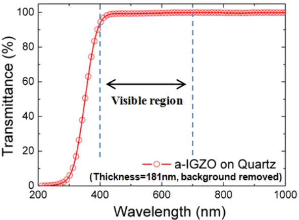
with the high transparency in the visible region and broader bandgap of 3.05eV,
opens a wide spectrum of applications such as transparent electronics and sensors.
This has significant properties which make it a much better material for TFT than
[image:26.612.175.471.246.464.2]a-Si and LTPS for large panel displays.
Figure 1.9: Transmittance of IGZO in the visible region of the spectrum
There are certain challenges to fabrication of IGZO TFTs on a large scale. From
previous studies, it was observed that the main problem to manufacture these were
their instabilities with thermal and bias stress. Shift in the threshold voltage under
thermal and bias stress has been observed. This instigated further studies in the
Figure 1.10: Comparison of different channel materials and their scalability along with their incorporation in the display industry [6]
The instability and non-uniformity issues could be compensated in LCDs by using
compensation circuit. But with the adoption of OLEDs which require high mobility
which emit light by electrical current injection, the a-Si TFTs could not support high
current devices. And hence it was necessary to move to a material with high mobility
as even the slightest variation in Vt of the TFT would cause significant variation in
brightness of the pixels. The luminance would vary by 16% for a +/- 1V change in
threshold voltage [2]. AOS were adopted for this purpose and their advantages over
a-Si had been mentioned in the previous sections. With increasing panel size and a
higher frame rate of greater than 120Hz required for improving video quality and 3D
capability, a few challenges need to be addressed. One of the major challenges is the
lack of charging time to apply video data to each pixel. As the pixel density increases
for large area displays, interconnects are scaled in x-direction. As the number of rows
increases, the time for charge transfer decreases to maintain a high image refresh
frequency. This can be addressed by either changing the driving architecture to
increase the turn on time or by improving the charging capability. Improvements in
the RC delay needs to be addressed while transitioning to higher definition panels.
With Al/Mo as the gate or Source/ drain metal, this becomes difficult and hence a
higher bulk thermal and electrical conductivities and is a promising candidate as a
replacement for Mo/Al as gate metal with appropriate process integration.
1.5
GOALS AND OBJECTIVES
The goal of this study is to investigate the influence of annealing conditions on copper
diffusion with and without a titanium interface layer. The objectives are
1. Verify method for copper adhesion.
2. Design of experiment for investigation with treatments that promote a
measur-able electrical response to metallic contaminants (i.e. VT shift, SS).
3. Measurement and interpretation of electrical characteristics.
4. Re-establish a baseline TFT process that produces consistent and reproducible
electrical characteristics and good stability. [Ensures electrical interpretation
is not influenced by process variation or instability which has been a recent
problem]
1.6
DOCUMENT OUTLINE
Chapter 1 summarizes the recent developments in the display industry and the role
of TFT in the structure of an active matrix display device. The different materials
adapted for thin film transistors have been summarized and the advantages of a-IGZO
over the other materials have been discussed briefly. Emphasis is given to motivation
of this work and the goal and objectives of the study.
Chapter 2 is dedicated to the electronic and material properties of IGZO. The
chem-ical structure of IGZO is discussed along with the conduction mechanism in the
with different treatments and processes of fabrication. This enhances designing
ex-periments for the devices to study the devices.
Chapter 3 discusses the detailed fabrication process for IGZO TFTs. The different
electrode configurations used for the study along with the various process parameters
changed to enhance the TFT performance has been discussed along with the changes
in its electrical characteristics. The change in the material properties of IGZO
moti-vated designing experiments to re-establish a baseline process for the fabrication of
the IGZO TFTs for display devices. The results obtained by varying different
param-eters such as IGZO thickness, passivation dielectric thickness and anneal conditions
are discussed and a new baseline process will be adopted for further study.This
chap-ter also discusses about the thermal stability of the bottom gate and double gate
devices. The results of the thermal stability of the devices fabricated with the
modi-fied baseline process was compared with the results of the devices fabricated with the
previously used baseline process. This was analyzed and discussed briefly.
Chapter 4 discusses the integration of copper as the bottom gate electrode. The
mo-tivation behind the incorporation of copper in the IGZO TFT is provided. Copper
being a low resistance material is an obvious replacement for molybdenum to obtain
low RC delay and faster transmission. But there are challenges to incorporating
cop-per in the process and this is discussed in detail in this chapter. Various process
variations such as gate stack, gate dielectric stack and anneal conditions are
sug-gested and experimented to see an enhancement in performance. The experimental
results with these variations are provided and compared with the baseline process
with molybdenum as the bottom gate electrode.
Chapter 5 provides a summary of work done to incorporate copper as the bottom
gate electrode. The process of re-establishing a baseline process and studying the
thermal stability of the devices to be able to adopt copper as the gate electrode for
ELECTRONIC AND MATERIAL PROPERTIES OF IGZO
IGZO has proven to be a promising candidate for the active channel material of
the TFT in FPDs. The role of TFT in AMLCD and AMOLED panels have been
discussed. The major advantage of using IGZO for large panel displays as discussed
previously is its low processing temperature and uniformity over a large area. In
this chapter we will dive deep into the structure and characteristics of the material
along with its conduction mechanism and TCAD model to better understand the
relationship between the electrical characteristics and the material defect state model.
Amorphous oxide semiconductors have mobility higher than a-Si due to the
ionic bonding of material. Also, they also have lower values for subthreshold swing
(SS) which promotes better overall performance of the device. The lower value for
SS and higher mobility are due to lower influence of trap states near the conduction
band.
2.1
MATERIAL PROPERTIES OF IGZO
IGZO is an n-type amorphous oxide semiconductor. The amorphous nature of the
material is due to the composition of the material. It is a ternary metal oxide with
In2O3, Ga2O3 and ZnO in the ratio of 1:1:2, resulting in an elemental In:Ga:Zn:O
Figure 2.1: Molecular structure of a-IGZO [7]
Amorphous semiconductors are expected to exhibit deteriorated performance
such as low mobility in comparison with the crystalline materials due to their strong
scattering of the disordered structure. Conduction mechanism in both covalent and
ionic amorphous semiconductor is studied.
[image:31.612.154.490.436.665.2]Chemical bond in covalent semiconductor such as a-Si is made up ofsp3orbitals
which have strong spatial directivity. Conduction in a-Si is due to overlap of these
highly directionalsp3 orbitals which are very sensitive to bond angle variation unlike
a crystalline material. The material possess short range order and follows carrier
hopping conduction mechanism where the electron is captured in a localized state
and re-emitted into extended states significantly affecting carrier mobility. Unlike
a-Si (covalent bonding), conduction in an ionic semiconductor material such as a-IGZO
is through band conduction [8]. The valence band is formed by filled p-orbitals of
oxygen anion and the conduction band is formed by empty s-orbitals of the heavy
metal cation. Charge transfer between these results in Madelung potential which is
shown in Fig 2.3. The distance between these bands (bandgap) is 3.2 eV with RF
sputtering technique. The wide band gap in the structure attributes to the optical
[image:32.612.183.463.404.519.2]transparency of the material[10].
Figure 2.3: Madelung potential resulted from the transfer of electrons from the valence band to the conduction band of amorphous oxide material (a-IGZO)[9][10]
The s-orbitals of the metal cations are spherically symmetric. A significant overlap
with the s orbitals of neighbouring metal cations provides a pathway for electron
transport. The spatial spread is determined by the principle quantum number, n, of
the metal cation. The larger values for n, such as in the case of post transition metals,
causes significant overlap between the metal cations which reduces the effective masses
material. The non-bonded metal cation (i.e. oxygen vacancy defect) produces a
shallow donor level which contributes to the free electron concentration. The oxygen
vacancy formation in IGZO has not been conclusive as there are different theories
proposed.
The dependence of Hall mobility on the compositional structure of the material
is discussed in detail by several groups. A study by Kamiya et-al. stated that Ga
concentration strongly influenced the Hall mobility and free carrier density. With
increase in Ga content, both the mobility and carrier density of the material decreased
due to the strong Ga-O bond. The strong bond is due to the strong ionic potential of
Ga+3 which suppresses electron injection. Zinc incorporated materials such as IZO
have the highest mobility in comparison with the other binary oxides[4]. However
to be adopted for TFTs, the free carrier concentration needs to be controlled. The
incorporation ofGa+3 suppressed the density of oxygen vacancies. Indium ion (In+3) provides electron transport path in the conduction band through its large 5s-orbital.
Amongst the three metal cations, In+3 is the only ion that meets the criteria of (n−1)d10ns0 of a heavy post transition metal cation.
Studies conducted by Kamiya et-al on the composition of the material is shown
in Fig 2.4. Thus from the above mentioned reasons, IGZO with elemental ratio of
Figure 2.4: Hall mobility dependence on composition of the material (a-IGZO)[11]
Strong ionic nature of bonding in this structure promotes formation of defects
easily due to the non-bonding of the transition metal ions with its neighboring ions.
This causes poor long-term stability and makes it difficult for doping owing to their
self- compensation effect. Studies have proved that the instability might be due
to grain boundary effects which deteriorates the short-range uniformity in a
poly-crystalline structure. Due to the amorphous nature of IGZO, grain boundary effect
2.2
CONDUCTION MECHANISM IN IGZO
Figure 2.5: Schematic illustration of conduction and electronic structure around conduc-tion band edge. This represents the percolaconduc-tion conducconduc-tion mechanism in IGZO where the electron path finds lower energy states to travel[12]. An arrow is an electron conduction path. (left bottom) potential distribution cross-section. Eth and EF denote threshold en-ergy at above which carrier moves freely and Fermi level, respectively. (Right) Density of state [13]
Controllability of the carrier concentration is critical in IGZO (amorphous oxide
semi-conductors in general) as they can easily form defects. The primary defects formed
during deposition are oxygen vacancies (Vo) which act as shallow donors in IGZO.
Hall mobility has a functional dependence on the carrier concentration and
tempera-ture. Thus, the mobility increases with increase in carrier concentration unlike that of
crystalline materials where the mobility decreases with increase in free carrier
concen-tration. This increase in mobility can be explained through a percolation conduction
model as seen in Fig 2.5. Due to the strong ionicity of oxides, both the conduction
band and valence band are formed by ionic species. As mentioned in the previous
section, the conduction band is formed by empty s-orbitals of the heavy transition
metal cations and valence band is formed by filled p-orbitals of oxygen anions. The
spherical symmetry of the s-orbital has a large spatial spread. This causes a
The oxygen vacancies defects (V0) are formed near the conduction band due to the
non-bonding of the transition metal ions with the neighboring ions. These V0 act as
shallow donors, typically generating free electrons as follows[13] [8] [12].
Vo→Vo2++ 2e
−
(2.1)
Figure 2.6: Generation of oxygen vacancy (Vo2+) and free electrons from the metal oxide whereM(+ 2) is the metal cation andO(−2) is the oxygen anion. [9][10]
This carrier concentration can be controlled by varying the deposition parameters
such as oxygen partial pressure or sputter power experimentally [15]. With increase
in oxygen partial pressure the density of oxygen vacancies and free electrons decreases
[15]. This confirms the source of free electrons as mentioned above in Eq 2.1.
Am-bient conditions during post metal annealing also has a significant influence on the
electronic properties of IGZO and the M-S contact behavior [19]. Optimum degree
of oxidant exposure during annealing with the right ambient conditions (time and
temperature) will result in reduction of defect state concentration [19]. The ability
to control the carrier concentration makes IGZO a good choice of material for TFTs
in display devices.
2.3
DENSITY OF STATES
The band structure of as-deposited a-IGZO with density of states distribution within
the bandgap is presented in Fig 2.7. Incomplete bonding is observed due to the
states can either be donor-like or acceptor-like. Since IGZO is an n-type channel
mate-rial, the focus here will be primarily on the sub-gap states near the conduction band
which influences the TFT characteristics. Density of sub-gap states can be
char-acterized by contributions from four defect distributions; acceptor-like exponential
function, acceptor-like Gaussian function, donor-like exponential function, donor-like
Gaussian function. The exponential functions are used to represent tail states and
the Gaussian function is used to represent deeper sub-gap states. The tail states in
the conduction band are observed due to the variation in bond angle of In-O. The
band tail states near the conduction band minimum are very wide, 80-150meV, with
these values close to Urbach energy [20]. The width of the band tail states of the
conduction band become smaller in the deeper bandgap region. Oxygen vacancies
act as donor-like states near in the conduction band. Change in the density of states
in this region will cause a shift in the threshold voltage. Increase in the density will
make the IGZO more conductive by generating more electrons and acts as metals
instead of a semiconductor. Fermi level lies 0.15eV below the conduction band
mini-mum and this shifts towards the conduction band when there is an increase in VGS.
This causes electron trapping in these states. The sub-gap density of states 0.15eV
below the conduction band are smaller which explains the higher mobility, small
sub-threshold swing and low operating voltage in a-IGZO TFTs. The amorphous nature
of the material breaks the coherent hybridization of 2p orbitals of Oxygen anion and
forms strongly localized states isolated from the valence band. The density of this
deep sub-gap states is >5X1020 cm−3 with a width of 1.5eV. The sub gap density of states of a-IGZO annealed at 400oC is 2-3 orders of magnitude lower than a-Si
near the conduction band which results in smaller subthreshold swing. This is an
Figure 2.7: Band structure of a-IGZO with tail states and Density of states (DOS) dis-tribution [14]
2.4
IGZO TFT CHARACTERISTICS
The performance of the device can be evaluated from various parameters obtained
from the output transfer characteristics of the device. On-currentIon and Off-current
Iof f are important characteristics to be determine for current devices like OLEDs
as Iof f is useful for determining the minimum power consumption of the device.
Threshold voltage is the gate voltage required to induce band bending at the surface
of the semiconductor layer. Threshold voltageVt of the device is the voltage at which
the TFT starts conducting and this is important as fluctuations in this value can
cause serious brightness variation in an OLED device which might further affect its
performance and lifetime. Hence it is important to understand the fundamentals of
physics to determine these parameters. In this section we will discuss in detail about
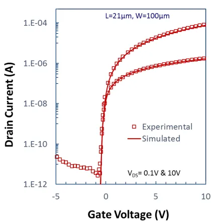
Figure 2.8: Comparison of the transfer characteristics of both experimental and simulated BG TFT with dimensions of L=21µmand W=100 µm
Fig 2.8 shows a comparison of the simulated and measured I-V characteristics of
bottom gate passivated device of 21 µm length and 100 µm width. The simulated
value matched very well with the measured data. The material and device model
used for TCAD simulation of these devices will be discussed in the next section.
2.5
MATERIAL MODELLING FOR TCAD SIMULATION
Device simulation aids in better understanding of the influence of defect states and
various other process parameters on the device operation. Visualization of the various
effects in the TFT channel and interface region is made possible to understand the
basic physics behind these. The presence of band tail states accounts for non-ideal
behavior in the electrical characteristics of IGZO TFTs which are not represented well
by the conventional models available. Extracting the basic TFT parameters such as
mobility and threshold voltage is difficult due to the presence of defect states and
gate voltage dependent source-drain resistance (RSD).
provides an excellent overlay to the measured characteristics. Silvaco Atlas was used
for simulating the TFTs interdigitated capacitors (IDC) and the establish material
and device model parameters. The density of states g (E) for both acceptor and
donor like band tail states and oxygen vacancy donor states defined by exponential
and Gaussian distributions are represented as follows
Where gT A(E) and gT D(E) are the density of acceptor-like conduction band tail
states and donor-like valence band tail states respectively. Ec and Ev are the energy
levels at the conduction and the valence band edge. NTA and NTD represent the
density of acceptor-like states in the tail distribution at the conduction band edge and
density of donor-like states in the tail distribution at the valence band edge. WTA
and WTD is the characteristic decay energy of the conduction and valence band-tail
states. gGD(E) is the density of donor-like states (oxygen vacancies). NGD, EGD and
WGD are the peak value, mean energy and energy standard deviation, respectively,
defining a Gaussian distribution for donor-like states, gGD(E) [15].
The non-ideal characteristics of the TFT were modelled by inclusion of interface
defects to have a reasonable fit with the measured data. In this case of a good device,
the influence of interface defects on the TFT characteristics was negligible and the
bulk state defects. The band tail state density at the valence band edge and the
donor-like valence band tail states do not influence the on state of the device.
To account for the defect states in a passivated device, additional parameters were
of IGZO and the dielectric. Fixed charge density of Nf = −1.9x1012cm−2 and a
Gaussian distribution of donor-like interface traps (Nvo) were adopted to provide
a reasonable match to the characteristics. These modified parameters were used
to account for threshold voltage shift. EGD and WGD values for interface traps
were consistent with that provided for bulk states; the peak of the distribution was
[image:41.612.130.519.268.429.2]adjusted to 2x1012cm−2/eV. The total integrated donor interface trapped charge state density NIT ∼5x1011cm−2 and a net back-channel surface state densityNSS ∼ −1.4x1012cm−2 was obtained.
Figure 2.9: Modified parameter values for material and device model in TCAD [10] [15]
The total space charge in the channel material due to oxygen vacancies integrated
over both energy and thickness of the film is Nbulk ∼2.5x1010cm−2. The influence of
interface charge over the TFT characteristics can be dominant in the case of non-ideal
IGZO TFT PROCESS DEFINITION AND BASELINE
PROCESS MODIFICATION
This chapter outlines the standard IGZO fabrication process in detail. Two different
electrode configurations, the bottom-gate (BG) and the double-gate (DG) structure
and their electrical characteristics are presented. Electrical characteristics of devices
tested recently were inconsistent with results previously established, and so this
de-viation became a significant piece of this investigation. It was observed that the
electrical operation of the TFTs varied from process runs done over several months,
with a notable shift towards depletion-mode operation. This suggests that the
ma-terial properties of IGZO had varied over this time period, hence experiments were
designed to vary parameters in the fabrication process such as IGZO sputter
condi-tions and thickness, passivation material thickness and anneal condicondi-tions. The results
obtained from the design of experiments were used to modify the baseline process for
fabrication, which was then used for further experiments in this study. The devices
fabricated using the modified baseline process were thermally stressed at high
tem-peratures of 140oC and 200oC to investigate the thermal stability of these devices.
3.1
TFT FABRICATION
A 6-inch silicon wafer with 6500 ˚A of thermally grown silicon dioxide is used as the
base substrate for processing to represent the fabrication of IGZO TFTs on glass.
For the bottom gate electrode, 50 nm of molybdenum is sputter deposited by
phys-ical vapor deposition using CVC601. Once sub-microtorr base pressure is achieved,
the sputter deposition is done in argon ambient at a pressure of 2.7 mT. An 8-inch
target was used at 1000 W power for 200 s to obtain the target thickness. The gate
electrode is then patterned using a GCA g-line stepper, and subtractive etched using
molybdenum etchant which is a combination of acetic, nitric and phosphoric acid.
The gate dielectric (100 nm SiO2) is deposited using plasma enhanced chemical
va-por deposition (PECVD) in an AMAT-P5000 with tetraethyl orthosilicate (TEOS)
and oxygen as precursors at 390oC. The oxide is then annealed (densified) in nitrogen
ambient at 600oC for 2 hours. After densification, 50 nm of IGZO is RF sputter
de-posited at Corning Incorporated using an AMAT Centura system. Reactive sputter
is done with the substrate temperature maintained at 200oC using a target
compo-sition of In2O3 : Ga2O3 : ZnO in the ratio of 1:1:2, in argon with oxygen partial
pressure of 7%. The IGZO is patterned and wet etched usingH2O: HCl in the ratio
of 6:1. Devices with and without back-channel passivation were fabricated. For an
un-passivated device, the gate contact cut is patterned and etched using BOE (10:1)
to make contact to the bottom gate. S/D patterning is done using negative resist
and then the metal is sputter deposited using the CVC601 in argon flow 20 sccm at
2.7 mT, using DC power of 200 W. A molybdenum/aluminum bilayer stack (each 50
nm thick) was used as the source/drain metal, where the molybdenum serves as the
contact metal and aluminum provides resistance to thermal oxidation during
anneal-ing. The metal is patterned using a lift off process done by subjecting the wafers to
then subjected to an anneal at 400oC for 30 minutes in nitrogen ambient, with an air
ramp down. This is done to reduce the IGZO conductivity by reducing the number
of oxygen vacancies and in turn reducing the electron concentration, thus providing
appropriate semiconducting properties for TFTs. For passivated devices, 100 nm
of passivation SiO2 is deposited following the S/D metal, using the AMAT-P5000
PECVD TEOS process. An anneal is done in an oxygen ambient at 400oC for 8hours
with a 5 hour ramp down. ALD alumina (10-15 nm) is deposited as an optional
bar-rier layer at 200oC. The substrates are immediately taken for ALD deposition after
annealing to minimize exposure to air ambient. The passivation open patterning is
then done to contact the electrode pads and wet etched using 10:1 BOE for 5minutes.
The devices are then ready for testing.
3.1.1 DIFFERENT ELECTRODE CONFIGURATION
Staggered and co-planar electrode configurations are used for TFT structures [22]
[23], but this study will focus on the staggered BG and DG arrangements. These two
configurations and their electrical characteristics will be discussed and analyzed.
3.1.1.1 BOTTOM GATE STRUCTURE
The staggered BG structure is shown in Fig 3.1. The TFT is typically fabricated
with a passivation dielectric, however devices without back-channel passivation were
Figure 3.1: Cross sectional view of a bottom gate configuration of IGZO TFT
Fig 3.2 shows the I-V characteristics of a passivated bottom gate device measured
using a HP4145 analyzer with a gate sweep of −5 V to +10 V and low drain bias of
[image:45.612.150.488.389.668.2]0.1 V and a high drain bias of 10 V.
The electrical characteristics of the BG TFT show a minor influence of interface
traps at the back-channel which appears as slight degradation in subthreshold
opera-tion. This can be overcome by the DG electrode configuration shown in Fig 3.3. Over
a year’s time the BG passivated devices demonstrated process drift, exhibiting poor
electrical characteristics such as poor subthreshold slope, DIBL (drain induced barrier
lowering) like separation on long channel devices. They exhibited the weakest ability
to overcome the influence of interface trap states and control the TFT operation.
Figure 3.3: Cross sectional view of a double gate configuration of IGZO TFT
3.1.1.2 DOUBLE GATE STRUCTURE
The DG device has a similar process of a bottom gate device with an additional top
gate electrode over the ALD passivation material. The top gate electrode is aluminum
which is thermally evaporated and patterned using a lift off process. Subtractive etch
was replaced with a lift off process to have a controlled patterning of the metal.
The double gate structure shows advantage over the bottom gate device as they
have better control of the back-channel layer which is prone to trap charges causing
instability of the device. A more detailed description of this instability is discussed
in the next section of the chapter. Figure 3.4 shows the I-V characteristics of a DG
low drain bias of 0.1 V and a high drain bias of 10 V.
Figure 3.4: Characteristics of a double gate IGZO TFT of L/W= 24/100µm
The transfer characteristics of the double gate device showed improvement of both
the on-state and off-state performance of the TFT due to improved electrostatics.
The presence of an additional top gate enhanced the performance of the device by
improving the SS from 260 mV/dec to 180 mV/dec and essentially a two-fold increase
in channel charge (i.e. drain current).
3.2
PROBLEM STATEMENT
The electrical operation of the TFTs varied from process runs done over several
months, with a notable shift towards depletion-mode operation. The BG passivated
charac-teristics on long channel devices; both indicative of back-channel charge and lack of
gate control. While the influence on DG devices was not as pronounced, this source
of variation had to be identified and suppressed. The focus initially shifted to the
BG unpassivated device process for baseline comparisons. It was observed in the I-V
characteristics of an un-passivated device that the standard anneal was not adequate
to reduce the sub-gap states in the channel region. The threshold voltage of the
de-vice was left shifted drastically. Ripening is the process of exposing the channel to
ambient environment; this promotes the self-passivation of high-density trap regions
at the back-channel [24]. The devices were left in ambient conditions for ripening
process. But after ripening it was observed that the devices seemed to behave like
an under annealed device with the threshold voltage left shifted from the ideal value
close to 0-V with significant trap associated barrier lowering (TABL) as seen in Fig
3.5. This effect is due to in-homogeneity of donor states at the topside IGZO
inter-face that presents regions with distinctly different effective charge levels In the case
of passivated bottom gate devices, the 8hrs anneal in O2 ambient at 400oC did not
suffice in reducing the number of oxygen vacancies in the channel and the interface.
Increased annealing did not seem to be effective in restoring the transfer
characteris-tics. This then steered us to the hypothesis that there could have been a change in
(a) (b)
Figure 3.5: Characteristics of an unpassivated BG TFTs with IGZO thickness of 50 nm whose L/W=12/24µminitial results tested on different days to observe the ripening effect in room ambient with a) standard anneal conditions b) L=24,12,6µmtested after aggressive annealing conditions .
Figure 3.5a is the characteristic response of unpassivated devices with standard
anneal in N2 ambient for 30 mins and ripening process. It is observed that these
devices even after 6 days of ripening in ambient does not yield good characteristics as
observed in Fig 1.8 whereas the 24 µmlength devices in the Fig 3.5b after aggressive
annealing conditions (30min inN2ambient, 1hr inO2 ambient with 4 hour ramp down
inO2) yielded good TFT characteristics with steep subthreshold and threshold voltage
of the device close to ideal value. These devices did not exhibit Trap Associated
Barrier Lowering,which is the mechanism to describe the long channel DIBL-like
separation as observed in Fig 3.5a but short channel devices of L=12 µm and 6 µm
showed significant TABL and left shift in the characteristics. This was conclusive of
(a) (b)
Figure 3.6: Characteristics of a) passivated BG (left) and b) DG (right) devices with channel length L=12 µmwith standard anneal conditions in O2 ambient for 8hrs at 400oC
The devices exhibited poor electrical characteristics with shallow SS and
signif-icant TABL in the case of passivated bottom gate device with standard O2 anneal
at 400oC for 8hrs as observed in Fig 3.6a. Whereas the double gate devices with
the same anneal conditions and without ALD capping layer exhibited good results as
shown in Fig 3.4.
3.3
DESIGN OF EXPERIMENTS ON FABRICATION OF
TFTs
The devices fabricated with the standard process parameters as stated in the above
section exhibited anomalies in their behavior that need to be addressed to yield
devices with good TFT characteristics as seen in Fig 3.2 and 3.4. The parameters that
influence these anomalies in the device behavior were, thickness of the channel layer,
Table 3.1: Design of experiments with IGZO thickness and oxygen partial pressure
Device Configuration IGZO thickness (nm) Oxygen partial pressure
BG 20 7%
BG 35 7%
BG 45 7%
BG 50 7%
BG 30 13%
BG 50 13%
to modify the electrical characteristics behavior of the TFT and their results.
3.3.1 IGZO THICKNESS AND BACKCHANNEL INTERFACE
The effect of channel thickness on the electrical characteristics of the TFT is
investi-gated in this section. Design of experiments (DOE) with various thicknesses of IGZO
and the oxygen partial pressure during deposition was proposed. The characteristic
response of the TFTs with the varying conditions will be discussed in detail.
Ta-ble 3.1 presents the different thickness along with the oxygen partial pressure varied
during deposition experimented in this study. Increasing the oxygen partial pressure
to 13% by doubling the gas flow was done to reduce the number of defects in the
channel (Vo). Increasing the partial pressure increased the deposition rate by 50%
thus rendering a thicker film. Thinner channel material was obtained by as-deposited
thin layer and back channel etching process. There was significant difference in the
Figure 3.7: I-V characteristics of BG passivated devices with different channel thicknesses of L/W=12/24 µm with 50 nmSiO2 with 4hr anneal inO2 ambient
From fig 3.7 it was observed that there was no significant change in the electrical
characteristics of the devices with IGZO thinned by wet etch process 20 nm and 38 nm
thickness in comparison with the 50 nm device. The thickness of the channel
mate-rial does not affect the SS but affects the threshold voltage of the device.However the
dependence of threshold voltage on thickness is questionable considering the
inconsis-tent shift shown in Fig. 3.7. This can be observed from the results obtained but there
is no significant variation in the threshold voltage. Devices with as-deposited
thin-ner channel material showed poor characteristics in comparison to the back-channel
etched devices. Wet etch of IGZO is critical and there was inconsistency in the
be-havior of these devices which is not well understood and hence 50nm as-deposited
Figure 3.8: IV characteristics of a BG passivated device of W/L of 24/12µmwith 50 nm IGZO annealed at 400oC for 8hrs in O2 ambient
Figure 3.8 shows that the electrical characteristics of the passivated BG device
with thinner passivation dielectric and standard 8hr anneal but these show poor
electrical characteristics with shallow SS. Whereas the BG device as seen in Fig 3.7
with 4hr anneal shows improved electrical behavior.
3.4
PASSIVATION AND ANNEAL CONDITIONS
Reducing the thickness of the channel material did not render significant improvement
in the electrical characteristics of the device. The experimentation was then focused
on the reduction of passivation dielectric thickness and the modification in anneal
conditions. From Fig 3.7 it was observed that reducing the passivation dielectric
improved the electrical characteristics of the device. Experiments were designed with
The design of experiments is for different IGZO thickness and anneal conditions are
tabulated in Table 3.2. Increasing the annealing was proven not to be effective at
restoring the electrical properties of the device as this depleted the devices further
(left shifting the I-V characteristics) and exhibited pronounced TABL (separation
between the high drain and low drain characteristics).
Table 3.2: Design of experiments with different passivation anneal conditions
Device Configuration IGZO thickness Passivation material Annealing conditions
BG passivated 20,30,50nm SiO2 + 10nm Al2O3 3-6 hrs at 400oC inO2ambient
Annealing in oxygen ambient is done to reduce the electron concentration by
reducing the number of sub-gap defect states in the channel material. From Fig 3.7
it was seen that reduction in anneal time to 4 hours, when in combination with the
thinner (50 nm) passivation oxide, had a significant significant affect in the reduction
of electron concentration which right shifted the characteristics. Anneal times were
varied from 3hrs to 6hrs to identify the ideal conditions for the stack mentioned in
(a) (b)
Figure 3.9: Transfer characteristics of BG passivated devices of under different anneal conditions a) 4hr anneal on a BG passivated device of L/W=6/24 µmb) 3hrO2 anneal on
BG passivated devices of L/W=6/24µm
It was observed from the results in Fig 3.9b that 3hr anneal has characteristics
similar to the 4hr anneal with threshold voltage of the device shifted further to the
right. Results suggest that the 3hr anneal is ideal for modifying the material
prop-erties of IGZO and improves the electrical characteristics of the device with right
shift in comparison to the 4hr anneal as seen in Fig 3.9b. It also reduces the time of
fabricating the device.
3.4.1 MODIFIED FABRICATION PROCESS FLOW
The results of the experimentation done in the previous section has helped re-establish
a new process for the fabrication of TFT to yield good devices. The modified process
conditions for the process will be summarized in this section to be used for future
ref-erence. The process parameters that will be modified are thickness of the passivation
the channel layer (IGZO) used was 50 nm with the oxygen partial pressure being 7%.
In the modified process, the thickness and deposition conditions of IGZO remained
the same. The S/D metal deposited is 50/50 nm of Mo/Al by sputter deposition
with the deposition conditions as mentioned in fabrication process. The devices are
then passivated with 50 nm of SiO2 deposited by PECVD with TEOS and oxygen
as precursors at 390oC. The anneal conditions were modified from 8hrs to 3hrs at
400oC in an O
2 ambient. The devices are then immediately deposited with another
passivation layer of 10 nmAl2O3 by ALD at 200oC. It is important to not subject the
device to ambient conditions with oxygen and water vapor as these when absorbed
act like donors in the channel region which will cause instability in the device. The
devices fabricated with these modified process parameters showed improvement in
the IV characteristics such as steeper subthreshold sweep, right shift in the
charac-teristics which is due to reduction in the number of oxygen vacancies which leads to
better control of the density of electron concentration in the channel region. The IV
characteristics of the devices fabricated with the modified process is shown in Fig
3.9b.
3.5
THERMAL INSTABILITY OF IGZO TFTs
It is well established that IGZO is extremely reactive to ambient conditions, both
during and after TFT fabrication. Long lifetime of the devices is a requirement for
display devices and hence stability of the TFTs is important. The stability of the
devices with thermal stress is important and must be studied as the devices degrade in
performance when subjected to elevated temperature (e.g. T 200oC) following TFT
fabrication during chip-on-glass attachment for the bonding mechanism. Thermal
stability of IGZO TFTs were previously studied at applied temperatures of 140oC and
200oC, as these temperatures were considered essential for process integration. When
the TFTs, both BG and DG were subject to 200oC on a hot plate with SiO
back-channel passivation, significant left shift in the IV characteristics of the BG TFT
was observed after an hour of stress. This was more pronounced in the DG devices
which upon stress for 20-min on a hot plate showed resistor-like behavior. These
results motivated further investigation as the devices showed stable characteristics
after the final passivation anneal at 400oC.
[image:57.612.116.521.222.429.2](a) (b)
Figure 3.10: a)BG and b)DG TFTs of L=24µmwithSiO2as the back-channel passivation
material which show degradation in performance when stressed on a hot plate at 200oC
An additional layer of capping between the SiO2 and aluminum was deposited
using atomic layer deposition at 200oC which was found to suppress the reaction of
water with the top gate. Both the BG and DG TFTs showed good stability when
the devices were passivated with an additional capping layer of 10 nm of Al2O3 using
(a)
[image:58.612.217.424.84.497.2](b)
Figure 3.11: a)BG and b) DG devices with 10 nm Al2O3 capping layer between
back-channel passivation dielectric and the top gate metal (aluminum)
3.5.1 THERMAL STRESS RESPONSE ON MODIFIED BASELINE
PRO-CESS
The devices fabricated with the modified baseline process both bottom gate and
(a) (b)
Figure 3.12: a) BG TFTs of L=4 µm and b) L=24 µm thermally stressed at various temperatures as indicated in the plot
From the Fig 3.12a it is observed that the bottom gate devices upon thermal stress
of up to 200oC showed stable behavior without any drastic shift in characteristics.
The thermal stability of these devices with the modified process is similar to the
results obtained with the old process conditions as mentioned in Fig-3.11a. There is
consistency in the device behavior of a BG device when subjected to thermal stress.
When the DG devices were subjected to thermal stress, both the short channel and
long channel devices degraded by significantly shifting to the left after 140oC hot
plate bake. After 200oC, the devices failed which can be observed in Fig 3.13. This is
inconsistent with the observations made in the previous section as shown in Fig-3.11
where the small channel devices are stable with thermal stress and the longer devices
(a) (b)
Figure 3.13: DG devices of a) L=4µmand b) L=24µmthermally stressed on a hot plate at various temperatures as indicated in the plot
There is difference in the behavior of the short channel and long channel device
as seen in Fig.3.13. The short channel devices of length 4 µm, when subjected to
140oC hot plate treatment causes a left shift in the characteristics of the device by
less than one volt whereas in the case of a longer channel device of L=24 µm shift
the characteristics is significant by almost
![Figure 1.1: Comparison of IV characteristics of TFTs with different active channel mate-rials [1]](https://thumb-us.123doks.com/thumbv2/123dok_us/25606.1987/17.612.182.469.79.303/figure-comparison-characteristics-tfts-dierent-active-channel-rials.webp)
![Figure 1.3: Structure of Liquid crystal display [3]](https://thumb-us.123doks.com/thumbv2/123dok_us/25606.1987/21.612.172.477.243.473/figure-structure-of-liquid-crystal-display.webp)
![Figure 1.4: Circuit diagram for pixel addressing in a) passive matrix LCD b) active matrixLCD [4]](https://thumb-us.123doks.com/thumbv2/123dok_us/25606.1987/22.612.152.500.432.569/figure-circuit-diagram-addressing-passive-matrix-active-matrixlcd.webp)
![Figure 1.7: Structure of the OLED stack [5]](https://thumb-us.123doks.com/thumbv2/123dok_us/25606.1987/24.612.249.397.73.164/figure-structure-of-the-oled-stack.webp)
![Figure 2.1: Molecular structure of a-IGZO [7]](https://thumb-us.123doks.com/thumbv2/123dok_us/25606.1987/31.612.154.490.436.665/figure-molecular-structure-of-a-igzo.webp)
![Figure 2.3: Madelung potential resulted from the transfer of electrons from the valenceband to the conduction band of amorphous oxide material (a-IGZO)[9][10]](https://thumb-us.123doks.com/thumbv2/123dok_us/25606.1987/32.612.183.463.404.519/madelung-potential-resulted-transfer-electrons-valenceband-conduction-amorphous.webp)
![Figure 2.7: Band structure of a-IGZO with tail states and Density of states (DOS) dis-tribution [14]](https://thumb-us.123doks.com/thumbv2/123dok_us/25606.1987/38.612.172.474.72.346/figure-band-structure-igzo-states-density-states-tribution.webp)
![Figure 2.9: Modified parameter values for material and device model in TCAD [10] [15]](https://thumb-us.123doks.com/thumbv2/123dok_us/25606.1987/41.612.130.519.268.429/figure-modied-parameter-values-material-device-model-tcad.webp)