ELECTRICAL AND OPTICAL INVESTIGATIONS OF BETA-GALLIUM OXIDE
Thesis by
Michael Paul Anthony
In Partial Fulfillment of the Requirements For the Degree of
Doctor of Philosophy
California Institute of Technology Pasadena, California
1972
ii
i i i
ACKNOWLEDGEMENT
My years as a graduate student at Caltech have been a period of great personal growth for me; I wish to express my enormous gratitude to my advisor, Professor Carver Mead, whose perseverance, encouragement, criticism and concern were literally invaluable.
Thanks are due especially to Ingrid Vierheilig, who provided help and encouragement as well as most of the typing of this thesis, as well as to Carol Norris and the other secretaries in the Electrical Engineering Department, almost all of whom helped at one time or another with the typing.
To the many others in the Department and the Institute who gave me help, knowledge, or inspiration over the years, I offer my thanks, especially to Professor Charles Wilts, who provided me, perhaps without knowing it, with a model of integrity which I will not soon forget.
iv
ABSTRACT
An
experimental investigation of the optical properties ofS
-gallium oxide has been carried out, covering the wavelength range 220-2500 nm.The refractive index and birefringence have been determined to about
±
1% accuracy over the range 270-2500 nm, by the use of a techniquebased on the occurrence of fringes in the transmission of a thin sample due to multiple internal reflections in the sample (ie., the "channelled spectrum" of the sample.)
The optical absorption coefficient has been determined over the range 220 - 300 nm, which range spans the fundamental absorption edge
Two techniques were uped in the absorption coefficient
determination: measurement of transmission of a thin sample, and
measurement of photocurrent from a Schottky barrier formed on the surface of a sample. Absorption coefficient was measured over a range from
5
10 to greater than 10 , to an accuracy of better than
±
20%. The absorption edge was found to be strongly polarization-dependent.I.
II.
Acknowledgment
Abstract
Introduction
Refractive Index
v
TABLE OF CONTENTS
iii iv
1 3
A. Analysis of Technique 1
B. Experimental Results 13
C. Refractiv~ Index for Another Propagation Direction 20
III. Absorption Edge 23
23
28 31 36 46
48 IV.
A. Transmission Measurement: Theory B. Transmission Measurement: Experiment C. Photocurrent Measurement: Theory D. Photocurrent Measurement: Experiment Conclusion
References Appendices
-1-I. Introduction
A. Background of this Investigation Gallium oxide, B-Ga
2
o
3, has been found(l)to be.a semiconductor with a band gap of approximately 4.SeV. Its crystal structure has beenexhaustively studied(2); the crystal is monoclinic (space group C2/m), with one excellent cleavage along the (100) plane and a much poorer
cleavage along the (001) plane. Reported optical investigations of B-Ga
2
o
3 include a brief measurement of the absorption edge(J) and . (4 5) rather detailed studies of photo- and cathode- ray luminescence ' .As reported by Lorentz, (l) the conductivity of B-Ga
2
o
3 is dependent on the atmosphere in which it is grown (for flame-fusion grown crystals) or later annealed at high temperature. In an effort to furtherinvestigate this phenomenon, a study of the electrical properties of vacuum-deposited metal contacts on the (100) cleavage faces was begun. The current-voltage and capacitance-voltage characteristics, and zero-bias photocurrent as a function of wavelength were measured with several different metals including Al, Au, Pt and Cu, and barrier heights were determined from these data. (For details of these
techniques, see the excellent review by C. A. Mead(6)). The barrier heights for Au and Pt were both approximately l.35V, and those for other metals showed the linear correlation with electronegativity of
(7)
the metal expected for a highly ionic semiconductor. In particular, the Al-Ga
2
o
3 barrier was sufficiently low to provide an ohmic contact at room temperature.-2-cleavage found in 6-Ga
2
o
3 afforded an opportunity for certain optical and electro-optical studies; these studies comprise the main topic of this thesis.B. General Comments on Experimental ParameteLS
Because of the excellent (100) cleavage, it is very easy to produce optically flat plates of S-Ga
2
o
3 with parallel faces and thickness ranging from <lµm to -lnun. The experimental samples used in this work were all grown by flame fusion(B) in a slightly reducing atmosphere, and had electronic concentrations in the range of0.5-18 -3
2xl0 cm . Sample sizes were limited by the size of boules that could be grown, and the maximum dimension of any sample was <O.Scm; most
were considerably smaller. All optical measurements, with one exception (see section II), were carried out with light propagating along the crystalline c-axis; that is, perpendicular to the easy cleavage described above. Most transmission measurements were performed in a Cary Model 14 UV/Visible/IR spectrophotometer; when polarized light was required, a Glan calcite-prism polarizer was used. The photocurrent measurements were made using a Gaertner quartz-prism monochromator
-3-II. Refractive Index
The refractive index of 6-Ga
2
o
3, for light incident parallel to the crystalline c-axis, was measured over the wavelength range 0.27-2.5 micrometers. The material was found to be birefringent: both principal values of refractive index and their difference weredetermined over this wavelength range. Because a rather unconventional measurement technique was used, an analytical discussion of this
technique is presented first, followed by a description of the actual experimental parameters and results.
A. Analysis of Technique
The refractive index was determined from interference fringes ("channelled spectrum") observed in the optical transmission of a nearly transparent sample in the form of a flat plate with parallel faces; these fringes occur due to multiple internal reflections within the sample. The transmittance, for normally-incident light of wave-length
A,
of a parallel-faced plate of material with complexrefractive index n
=
n+
ik and thickness d is(9)T
-47rkd e
-A
(where
o
is a function of k and n, of order k/lOn fork$ n).
-5-kd
*
In the limit of negligible ahsorption (k << n and~ <<l), this
equation reduces to
T 1
(2) 2
e
n -1 )2 . 2 (2nnd)1
+ - -
sin ~2n I\
This form of the transmittance equation reveals the existence of
periodic maxima and minima in T (i.e., interference fringes) as a
function of
A
according to the condition2n(>.) d
>. m (3)
where m, the interference order, is integral for a transmission maximum
and half-integral for a minimum. (lO) An example of a transmission
spectrum exhibiting such behavior is shown in Fig. 1. (The data shown
are a plot of log T vs. A made on a Cary Model 14 Spectrophotometer,
with a sample of Ga
2
o
3 of thickness 7.03 micrometers, approximately1 mm x 3 mm in area).
While the value of refractive index as a function of wavelength
is inherent in such a plot, as indicated by equation (3), there are
practical difficulties in extracting it from the raw data. First, the
sample thickness d must be determined; since it comes into equation (3)
as a linear factor, the precision with which it can be determined
directly limits the precision of the determination of n. Second, the
*
This approximation is valid throughout the wavelength range used for
-6-continuity of the plot in Fig. 1 guarantees that we know the relative
orders of all fringes detected, but provides no clue as to the
absolute fringe order. That is, if the order of the first fringe (the
one occurring at largest wavelength) is m
1, then
we
know that theorder of the second fringe is
(4)
and similarly for all other fringes observed; however, the transmission
plot does not unequivocally indicate the order of the first fringe.
Hence, if some likely value M
1 is chosen (based, for example on some
other estimate of refractive index), it may well be in error by some
integer M • In that case all fringe orders will be in error by that
0
same additive constant.
The first difficulty can be overcome for all samples if the
thickness of any one sample can be independently determined by any
method. Taking m to be a continuous function of wavelength, we can obtain m(A) for a given sample at any wavelength A by interpolation
from the integral values actually measured. Then, for two samples,
I and II, of thicknesses d
1 and d11, and for any two wavelengths
A and AB, we have from equation (3) :
a
m1(A) - ml (Ab)
[
n(),,l
nC\l
]
(Sa)2d
-Ab
I A
a
and
f
n(A) n(\)
J
(Sb)mrr°') -
~r(\)
= 2dII
-7-and, by dividing (Sb) by (Sa),
dII mII(),a) - mr1C\ )
dr ml ().,a) - mr(\)
(Sc)
Since any additive error in fringe order will cancel in the subtractions,
this equation yields the ratio of the two sample thicknesses directly
from the data obtainable from a transmission plot like Fig. 1. (In
practice the data from a number of wavelength points can be used in
equation (Sc) and the results averaged to obtain a more accurate value
of the thickness ratio: see appendix A).
The second difficulty can be overcome if a sufficiently thin
sample is available. If, for a given sample, an arbitrary order
assignment is made, as discussed above, we have a set of wavelengths
Ai' at which fringes occur, and associated with each fringe a relative
order M. which differs from the actual absolute fringe order m. by
1. 1.
some unknown M • That is 0
m.
1. M. 1.
+
M 0 (6)for all fringes i . Then, noting that equation (3) can be solved to yield
n(A.) =
1.
m.A.
1. 1.
2d
at each fringe, we can define a "pseudo-index" N(A) based on the
assigned orders M.: 1.
M.A.
1. 1. 2d
(7)
-8-This "pseudo-index" of refraction corresponds to a family of curves, represented schematically in fig. 2, with the unknown integer "offset" M
0 (or, correspondingly, the known choice of 1st-fringe order, M1) as a parameter. One of these curves, the one for which M
=
0, is the0
true refractive index; the others differ from it at any wavelength A by M A/2d. For sufficiently thin samples the linear dependence of this
0
error term on A will overwhelm the actual variation of refractive index with A; then the curve next above the correct n(A) will show a dispersion
of the wrong sign (N(A) increasing with A) while the next lower curve will pass below N(A)
=
1. Since both of these conditions are impossible on basic physical grounds, the actual refractive index, lying between thetwo N(A) choices just discussed, will be unequivocally indicated. One other test for the correct choice of absolute fringe order exists, if several samples of differing thicknesses are available. For each sample, we can plot a family of N(A) curves like the set shown in fig. 2. One curve of each set is the actual refractive index n(A), and this curve should be the same for all samples. Thus if the N(A)
families for two samples are superimposed, one curve from one family and one from the other should coincide, these being the correct refractive index, for which in both cases M
=
0. The next curve up0
A
in each of the two families will be spaced from n(A) by
2d; since the thickness of the samples are presumed different, the spacings will also differ, and the next curves up and down will not coincide. If the sample thicknesses are not rationally related, in fact, no N(A) curves other than those for whi.ch M
=
0 will coincide. Thus again, the0
[image:13.553.6.540.26.746.2]z
~
>-'
WAVELENGTH
M
==+20
+l
0
-1
I
l.D
I
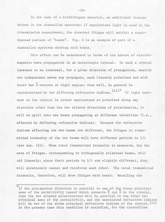
-10-In the case of a birefringent material, an additional feature arises in tl1e channelled spectrwn: if unpolarized light is used in the
transmission measurement, the observed fringes will exhibit a super
-imposed pattern of "beats". Fig. 3 is an example crf part of a
channelled spectrum showing such beats.
This effect can be understood in terms of the nature of electro
-magnetic wave propagation in an anisotropic crystal. In such a crystal
(assumed to be lossless), for a given direction of propagation, exactly
two independent waves may propagate, each linearly polarized and with
+
their two D vectors at right angles; they will, in general be
• • (ll))'C
characterized by two differing refractive indices. If light
inci-dent on the crystal is either unpolarized or polarized along any
direction other than the two allowed directions of polarization, it
will be split into two beams propagating at different velocities (i.e.,
affected by differing refractive indices). Because the refractive
indices affecting the two beams are different, the fringes in
trans-mitted intensity of the two beams will have different periods in l/A
(see eqn. (2)). When total transmitted intensity is measured, the two
sets of fringes, corresponding to orthogonally polarized beams, will
add linearly; since their periods in l/A are slightly different, they
will alternately cancel and reinforce each other. The total transmitted
intensity, therefore, will show fringes with beats. Recalling the
*
If the propagation direction is parallel to one+of th~ three principalaxes of the permittivity tensor which connects E and D in the crystal,
then the two allowed polari zations will be parallel to the other two
principal axes of the permittivity, and the associated refractive indices
will be two of the three principal refractive indices of the crysta1.(ll)
[image:15.562.11.544.24.744.2]W
~
I ,n
,
,-11111\
il
1
'
111
' '
'
.
,I
:
:
~
-
~
1±-.
I
i
I
i
i
!
!
I
!
i
!
.
_1 ..--
1
-
--i~J
l
I
·
J_j_r~-
~--.L
I
_
+-~-~--~-+-
i
-1
-
; :
<! ::J - ---H-T-
-,
-·-i
·
~-
,-
,---,-
·
-+--1
-
-
-
T--f-
~
.I
: - rI
-
~
I
. . ' i(.)1I
l1
V\
·
t~
''
•
I-·
v
:
I ! ,. .... 1 . : , . :.
I~
,rvv
·
f\l\
l,.~
.
• ,I- >,
1
. , • , • . • , ! V ,V ":"l' I · ' · • 'I
- '- • I I ' I i , I l • .J___ . . ! - · ·: -.. -,--- ---- . - . - \ I I .
~ ~ --~--+---!-'---,-
...
Ll
--
i
--
1
--
..
1--1··1 ·.-· ---
·-
·i-r
-
1 1
!
1 ' I I II
I '
;
iil
!I
i I<!) z _o ·"=
·
I
+I
•
!
:
j_
.
I . ! II
II
I I ' I!
! I _; . . . --- - ' - - - ' ·-I ' I
J
I ! ,_LJ_J __
1 ___J_,
__
l. ___ j_J
..
J
~---
-·
--··r
-"---~
--
~-
--;--
·-- :<! \... ___ : J ___ J_ .. _ -- -·
:
--,-+-·-+--
i -·-l·---;----, -- - i ' 'f
I ! t' 0 ' I I . .0::: <! ' I i : I :y.) I ' I . I .
I- ~
0.325 .0.320 0.315
WAVELENGTH (microrne1ers)
FIGURE 3. Example of channelled spectrum showing beats due to birefringence.
0.310
I
I-'
[image:16.771.20.751.15.537.2]
-12-relationship between fringe order, wavelength, refractive index and thickness which was derived earlier (eqn. (7)), we can see that for each of the two independent polarizations (referred to here by the subscripts 1 and 2) , fringes obey the conditions .
(9a)
(9b)
Thus at a particular wavelength
A
where a fringe reinforcement or cancellation (beat maximum or minimum) is observed, we must haveton _ (10)
with tom an integer for reinforcement and half-integer for cancellation.
This equation, in obvious analogy to equation (3), gives us bire-fringence ton as a function of wavelength from the wavelengths at which beats occur in the channelled spectrum.
An alternative method of determining birefringence, which is also capable of identifying the crystalline directions associated with the larger and smaller refractive indices, is the use of polarized light for the transmission measurement. According to the above analysis, an
-13-for which no beats occur, one can determine the directions in the
crystal along which the principal axes of the permittivity lie, and
*
the principal values of refractive index which correspond to them.
Birefringence can be calculated from such data, being simply the
difference of the two principal refractive indices at each wavelength.
B. Experimental Results
In the present work, the optical transmission of a number of
samples, ranging in thickness from 0.86 to 55.3 µm, was measured over
the wavelength range 0.27 to 2.5 µm. The transmission spectra of all
samples exhibited the interference fringes described in part A; five
samples, spanning the thickness range, were selected for detailed
analysis. For the purposes of the following discussion, they will be
identified as:
No. 1: thickness 34.27 micrometers
No. 2:
"
7.031"
No. 3:
"
0.860"
No. 4:
"
1. 21"
No. 5:
"
55.35"
For these samples, transmission was measured using both unpolarized
*
Beats in the transmission fringe system could also occur if the sample whose transmission was being measured had a step separating two areasof uniform but differing thickness. Beats due to such a cause would
not, however, depend at all upon the polarization of the incident beam;
-14-light, over the entire wavelength range, and polarized light* over the range 0.27 to 2.1 µm. The measurements were all made using the Cary Spectrophotometer. The wavelengths of occurrence of all fringes, both maxima and minima, were determined for all samples.
Sample thicknesses were calculated on the basis of equation (Sc) using the procedure explained in detail in Appendix A; the single independent thickness determination required was performed on sample No. 1 using X-ray absorption, by the following procedure. A metal mask of sufficient thickness to completely absorb the CuKa radiation employed was prepared, with an aperture which could be completely covered by sample No. 1. Transmitted X-ray intensity was measured with and without the sample present across the aperture. Using the known(2) absorption coefficient of 299 cm-l of S-Ga
2
o
3 for CuKa radia-tion, the sample's thickness was calculated to be 34.27 ± 0.10 micro-meters. (The probable error is based on X-ray counting statistics). Since this measurement is the basis of all thickness values used in this work, the probable error assigned above, amounting to+ 0.3%, appliesto the entire refractive index determination.
The experimental transmission spectra obtained differ in one respect from the theoretical ·form of eq. (2): due to the finite wave-length resolution of the spectrometer and to the convergence of the beam at the sample, a slight 11
averaging11
over. A. and d occurs·, with the result that fringe amplitude is not as great as that predicted by Eq. (2). Thus
-15-the fringe amplitude cannot be used as an independent measurement of n. As discussed in part A of this section, it is necessary, in
order to use the transmission fringe data to calculate refractive index, to determine for some sample the absolute order o{ the observed fringes. The method, described there, of plotting against wavelength the "pseudo refractive index" resulting from various probable choices of order, was applied to both samples No. 3 and No. 4. The resulting plots are
displayed in Fig. 4a. (The experimental data shown here are in exact analogy with the hypothetical data shown in Fig. 2). The upper curves for both samples, and the lower one for No. 3, can be ruled out on the basis of non-physical behavior, as discussed in part A of this section; in addition, the two samples yield a coincidence only for the center
choice for each. Thus, both criteria described in part A indicate the center curve to be the actual refractive index n(A.). In fig. 4b, the central set of data from fig. 4a is replotted on an expanded refractive index scale, along with the three adjacent N(A) curves for sample No. 2 which bracket it. The spacing between adjacent N(A) curves for sample No. 2 is much smaller than that between the N(A) curves for either
sample No. 3 or No. 4, due to the much greater thickness of sample No. 2. By the argument just employed, the N(A) curve for sample No. 2 which matches the n(A) values from No. 3 and 4 must be the M
=
0 choice for0
that sample; even with the considerable scatter of the data from the thinner samples, the choice for No. 2 is unambiguously ·the center one shown.
-17-spec tra very noisy. This noise led to difficulty in assigning an
accurate wavelength to each fringe, and thus to the scatter in n(A)
which is seen in fig. 4. Sample No. 2 (as well as No. 1 and No. 5) are
large enough to provide spectra with negligible noise, and therefore
very scatter-free N(A) curves. Therefore, once the choice of M
1 was
made for sample No. 2 as described above, no difficulty was
encountered in correspondingly choosing for the thicker samples.
Unpolarized light, yielding an n(A) which is an average over
birefringence, was used for the above data because the loss of 1/2 in
intensity due to a polarizer made measurements on samples No. 3 and
No. 4 unusably noisy. However, with the thicker and larger-area sample~
the intensity loss was tolerable, and a Glan calcite-prism polarizer
was used in the wavelength range 0.27 - 2.1 micrometers to resolve the
principal refractive indices. Beyond 2.1 micrometers, transmittance
of the polarizer became too irregular with wavelength to permit
trans-mitted intensity variations due to interference in the sample to be
distinguished; hence unpolarized light was used in this region for all
samples.
The crystalline directions associated with the principal
refrac-tive indices were found using the procedure described in part A of this
section: the polarizer was rotated with respect to the sample, until
a direction was found for which no beats occurred in the channelled
spectrum. Because no precise angle-measuring apparatus could be
installed in the sample chamber of the Cary Spectrophotometer, and
because the no-beat condition is not sharply defined, then directions
are known to only about* 10°. Within that accuracy the principal
crystalline b-axis.
-18-In monoclinic crystals the directions of the principal axes of
permittivity may in general vary with wavelength; that is, the crystal
h .b. . 1 d. . . (l3) I h . h d.
may ex 1 1t ax1a 1spers1on. n t e present instance, t e 1rec-tions indicated by the beat-elimination procedure w·ere constant over
the wavelength range (0.28 ~m to 0.43 µm) where beats occurred in the thickest sample used. In order to ascertain the directions of the
principal axes for wavelengths larger than 0.43 µm, use was made of the fact that light propagating with polarization other than one of the
allowed directions (in this case, the principal directions) should
show a channelled spectrum corresponding to some "average" refractive
index between the two principal values. For this reason, a polarization
direction which yields a value of n_(),) which is either a maximum or
minimum at a given wavelength must be one of the two allowed (principal)
directions. The principal directions were determined using this
criterion at A
=
1.95 µm, and were found to be identical to those foundin the A< .43 µm region, to within± 10°.
With the directions of the principal refractive indices thus
established, n (A) and n (A) (the subscripts referring to the
cryst-11 J_
alline b-axis) were measured from
A =
0.27 µm toA =
2.1 µm onsamples No. 1 and No. 2. The "average" refractive index resulting from unpolarized light was measured out to
A
=
2.5 µm. The results of these measurements, which constitute the final results of this refractiveindex determination, are plotted in fig. 5. Data from both samples are
plotted; they are not distinguished, since they match to within the
resolution of this plot, which is considerably less than the absolute
probable error of the measurement.
::0 rn
,,
::0 ::<> n - I ~ < rn ~ z CJ r'1 >< 2.202 .10
2.00
l. 90
1.80 ....
,•
..
~.
..
.··
....
··.
...
..
..
..
.
...
.
...
.
.
. .. ...
. .
. .
r
• 0 0 0
'--"
J
l I I , I I I I. I I I I I IL.
1
I0.5 l.O l. 5 2.0
~J/\V[LENGTll (mi cromcters)
FIGURE 5. Refractive index of Ga
2
o
3 vs. wavelength.UNPOLARIZED
0 0 0 0 0 0
01
l-~·~L
-~--I
t-'
\0
-20
-de termined from the wavelengths of occurrence of "beats" in fringe
systems obtained with unpolarized light, as well as directly from the polarized-light of fig. 5. Such "beat" data from two samples is considered here: samples No. 2 and 5. Only one fringe cancellation occurred in the spectrum of sample No. 2 before the absorption edge was reached: it occurred at 0.3225 micrometers. Since no cancellation occurred at longer wavelength, this one must correspond to the lowest
fringe order difference capable of yielding a cancellation: ~m
=
1/2. The first cancellation in"the spectrum of sample No. 5 occurs at 0.41325 µm, and the second at 0.37585 µm. It can be seen in fig. 5 that the two principal refractive indices cross over between these two w velengths; hence, J~mJ in both cases must be 1/2; (the orderdifference, of course, changes sign). Subsequent cancellations were assigned order differences of 3/2, 5/2, etc. The resulting values of ~n calculated from eq. (10) are plotted in fig. 6. This figure shows nl - n
II
calculated from the data shown in fig. 5 (solid dots) along with lm derived, as just explained, from the beat data (open points). The two sets of data are seen to be in substantial agreement.C. Refractive Index for .Another Propagation Direction In S-Ga
2
o
3, the cleavage perpendicular to the c-axis is the only one which yields surfaces of sufficient perfection for interference measurements of the type just described. However, a minor cleavage exists along the (001) planes, and a sample was produced which had two reasonably flat faces along these planes, over an area about 0.02 mm square. An extremely sharp grid of lines was viewed through the sampleco ,_. ;;o IT1
,,
;u ,_. ::<:: G) IT1 ::z ( } IT1 ::l I-I ::l0.0
6
--o
r
-0.0
4
-0.0
2
-..
0.0
-0 0e
0 0 0t
0 @Oo
O
o
o
o
0
:r
o
@
0
Ci.
"BEAT" DATA 0 POLARIZr:D I.IGllT 0
.. , () 0
ooc.:Jo c"
o
0 0 0 0© 0
-
0.02
-i
I
II
I=i
I
II
II
lt
0
.30
0.40
0.50
0.
5
l.o
1.
5
2.0
WAV
E
LEN
GTH
(
m
i
crometers
)
FIGURE 6. Birefringence of Ga
2
o
3 vs. wavelength.I
N
I-'
[image:26.769.16.749.15.519.2]
-22-rotated. If the sample exhibited birefringence for light propagating
in this direction, the image of the grid should show splitting; this
was not detectable. For comparison, the same sample held so that the
view was along the c-axis showed very obvious splitting of the image.
It is estimated on this basis that birefringence for light propagation
.
-23-III. Absorption Edge
The optical absorption of B-Ga
2
o
3 was investigated in the vicinity of a strong absorption edge at about 4.8 eV. (0.25 µm) which has previously(3) been associated with the electronic bandgap of the material. In this investigation two experimental techniques were used:(1) a conventional measurement of the transmittance of a plate of the material as a function of wavelength of incident light, which is a direct measurement of the optical absorption coefficient a , and (2) measurement of short-circuit photocurrent generated by light inci-dent on a Schottky surface-barrier fabricated on the material, from which a can be inferred if the optical absorption is assumed to be
due to an electronic valence-to-conduction-band excitation.
In parts A and C below, these two experimental techniques will be described and analyzed, and in parts B and D the respective experi-mental results will be presented and discussed.
A. Transmission Measurement: Theory
This measurement can be regarded as an extension of the measure-ment discussed in Section II into a wavelength range where the
condi-tions assumed there, k << n and kd/A << 1, no longer apply. Equivalently, one may say that absorption, as well as reflection, contributes to the difference between incident and transmitted inten-sity.
-24-thick that the "averaging" of the argument of the cosine term in equation (1) due to beam convergence and spectrophotometer resolution completely washed out the interference fringes disc~ssed in Section II. This effect can be taken into account theoretically by finding an "average" value of the transmittance expressed by equation (1):
specifically, the integral of T over one cycle of the cosine term, divided by 2~ , is such an average. Performing the indicated integral (a standard form) yields the average, or "smeared" transmittance at a wavelength A :
(11)
(This expression will be used in evaluating transmittance data even from samples which do exhibit fringes at or beyond the absorption edge; for such samples the experimental "average transmittance" will
be taken as the midline through the rapid fluctuations of T due to interference. Even for the thinnest sample used in this determination of a , the error in a resulting from this procedure is estimated to be less than one percent.)
Equation (11) gives the transmittance of an ideal uniform sample in a uniform beam, in terms of the sample refractive index and extinction coefficient, and the wavelength. However, the actual
experiment is carried out with a sample of finite size in a non-uniform spectrophotometer beam. Thus, equation (11) must be modified to
-25-Since the spectrophotometer beam was much larger in area than
any available samples, it was necessary to mask the beam to the sample
size and shape; in addition several samples had imperfections (bubbles
and other inclusions) which effectively masked additional beam area
and subtracted from incident intensity. This situation is depicted
in Fig. 7. In order to take into account the losses of beam power
(which is the quantity actually measured in the spectrophotometer)
due to the opaque parts of the mask and sample, or, in other words,
to establish a baseline for the transmittance measurement, the power
transmitted through the sample-plus-mask structure was measured in a
wavelength range where absorption contributed negligibly to beam
power losses. At such wavelengths the average transmittance given by
equation (11) reduces to the simple limiting form
T
=
(12)which can be evaluated at the wavelengths of interest by using the
n(A) data from Section II. In the more general case of equation (11)
as well as the limit of equation (12), the ratio of power transmitted
by the sample-mask structure to incident power, here labelled sample
transmission T will be smaller than the ideal sample
transmit-tance T by a multiplicative constant y which accounts for the
occluded beam area. Since T can be measured, and T calculated,
- --INCIDENT BEAM
.
---....__METAL MASK
SAMPLE
n
. I J~
_
r
=~
r
OCCLUSION
IN SAMPLE
... ..
-TRANSMITTED
BEAM
FIGU!tE 7.
Schematjc representation of sGmple and beam geometry in transmission measurement.J
N Cl"
accordingly applies), y
-27-*
can be determined for each sample. We
then have, for all wavelengths, the sample transmission given by:
T ()..)
-4TikdfA
e
(13)
Having experimentally determined y for a given sample, and measured
T
over the wavelength range in which sample absorption is to be determined, i t is necessary to apply equation (13) to theexper-imental data in such a way as to extract a value of a(A) , the quantity sought. The extinction coefficient k is the only unknown in equation (13); since this equation is transcendental, i t was
decided to extract k by an iterative procedure. Newton's method was
chosen, as being the simplest method available, and quite adequate to
the computation. Finally, a was calculated from k using the definition
(14)
This determination of a becomes uncertain in two limits.·
(1) ad << 1 . In this case, the absorption is negligible compared
to reflection and other beam power losses; hence, a slight error in
n(A) or y , for example, will produce a large error in the calculated
*
The value of y actually depends on the position of the sample inthe spectrophotometer beam, since the intensity profile of the beam
is not uniform. However, the transmission measurements used to calculate y and a were carried out as a single experimental
"run" with the sample fixed in position in the spectrophotometer during the entire measurement. Therefore the calculated value of
-28
-value of a .
(2) ad >> 1 . In this case, nearly all the light entering the sample
is absorbed, and scattered light in the spectrophotometer and sample
fluorescence become important in comparison with transmitted light,
leading to an apparent reduction of a below its actual value. In
order to obtain values of a over an appreciable range, i t is there
-fore necessary to employ several samples of differing thickness, each
contributing values of a around the point a ~ l/d .
By choosing sample thicknesses appropriately, a continuous
reliable curve of
in a .
a vs A can be obtained over a considerable range
B. Transmission Measurement: Experiment
Four samples were used in this measurement, with thicknesses
as follows:
No. 1:
No. 2:
No. 6:
No. 7:
thickness
II
II
II
34.27 µm
7.031 ]Jm
419.6 ]Jm
942.7 ]Jm
The first two samples were used also in Section II of this work and the
method used to determine their thicknesses is described there. The
thicknesses of the other two samples were measured using an "electronic
micrometer," a mechanical micrometer equipped with a spherical anvil
(of radius 'VQ.5 mm) and an electronic strain sensor for detecting
-29-apparatus is estimated to be accurate to ± 2 µm.
In the transmission measurements on these samples, the proce-dure described in part
A
above was used. Each sample, mounted on ametal mask which passed light only through the usable area of the sample, was held rigidly in the spectrophotometer beam, with a Glan
prism mounted just ahead of it in the beam. The transmission of this combination was measured from about 4000R to a wavelength sufficiently
short that the transmitted beam power was too small for the
spectra-photometer to detect. (This cutoff wavelength varied with sample
thickness.) These raw transmission data were first normalized by the
measured transmission of the Glan prism alone, which also took into
account any baseline irregularity of the spectrophotometer itself.
The normalized transmission from 4000R down to the onset of strong absorption (between about 2900R and 2550R for the various samples) was
used, together with the refractive index data reported in Section II,
to calculate the effective ratio of sample area to beam area y . Then
the remainder of the transmission data, in conjunction with y and the
known refractive index*, were used in the solution of equation (13) for
k(A) • Finally, a(A) was calculated using equation (14).
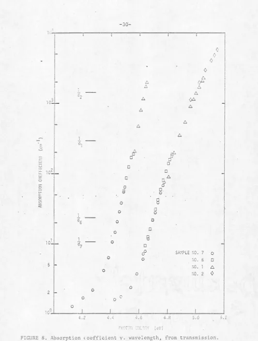
The results of the measurements are shown in Fig. 8. Two curves
of a vs hv are shown, as it was found that a depended on the
*
In the case of sample No. 2, the measured refractive index data had to be extrapolated in order to complete the calculation of a at the shortest wavelengths usable. SinceT
depends exponentially on ad and only linearly on n , the error from this extrapolation is-30
-1 ti I I
I
() ()0
()
~
6.<ft
.6. 6.
1
d2 6
10~ ,__ 6
06
-6 6 6 -6 ~ I dl u~
8-
;!:-0 w
~-102
I
0
LJ
0
u 0
-
0
'-'--T
-w L:;,.
~ !J
0
10
z
0 0
0
0
t- 13 0
0
-
-De: 08
(/') 0 c:i <0 0 0
d6 0 0
-0
0
10~ l
8
-
d7 0 0-00 S/l.MPLE NO. 7 0
0 0 rw.
6 0
5 ~
NO. 1 /::::,.
0
¢
0 ilO. 2
0 0
2 ,_
0 0 0
0
100 I I I I
4.2 4.4 4.6 4.8 5.0 5.2
(eV)
[image:35.561.14.547.17.720.2]-31-polarization of the incident light with respect to the crystalline
axes. Specifically, it was found that unless polarization was
oriented either parallel or perpendicular to the crystalline b-axis
(within about ±5°) the absorption edge exhibited a shoulder due to the
absorption of essentially all light of one polarization before any
*
light of the other polarization was absorbed. Thus two
characteristic directions of polarization for absorption were found,
which are in fact coincident with the optic axes found in the refrac
-tive index detennination (see Section II). The values of a vs. hV
for these two directions are the ones shown in Fig. 8.
Points from the four samples are distinguished in Fig. 8,
showing the range of values of a contributed by each sample. In
addition, the reciprocals of the four sample thicknesses are indicated.
As expected from the discussion in part A above, of the limitations on
the determination at the limits e ad -+ 1 and e ad << 1 ' the
reciprocal thickness of each sample falls approximately. in the middle
of the range of a values contributed by that sample.
C. Photocurrent Measurement: Theory
If the absorption edge being investigated is in fact due to
the electronic bandg_ap of !3-Ga
2
o
3 , then each photon absorbed by thecrystal in this wavelength range should result in an electron being
excited from a state in the valence band to one in the conduction band.
If a means can be provided for collecting these optically-excited
*This shoulder was observed by Tippins (J) who used unpolarized light
in his transmission measurement, but the polarization-dependence of
-32-elec trons, then the absorption of light by the crystal can be measured
indirectly, by measuring photocurrent.
A Schottky barrier formed on the surface of the sample by the
disposition of a layer of metal is one means of collecting
photo-generated electrons. The properties of such surface barriers have
been reviewed in detail (6); the relevant points will be briefly men
-tioned here.
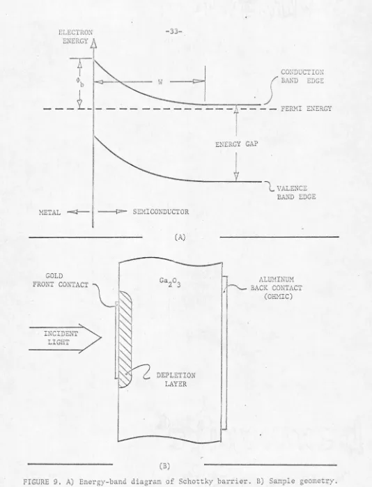
The energy-band diagram of a metal-semiconductor surface
barrier (Schottky barrier) is shown in Fig. 9a, and the corresponding
physical structure in Fig. 9b. The structure is depicted for the
condition of zero applied bias, in other words, at equilibrium. The
conduction and valence bands of the semiconductor, and the Fermi energy
(which is constant throughout the structure) are labeled; the
semicon-ductor is represented as strongly n-type. The important features of
this structure for the present discussion are the potential barrier of
height ¢B between the semiconductor and the metal, and; the "depletion
layer" which extends from the metal-semiconductor interface to a depth
w into the semiconductor. The depletion layer is characterized by
the absence of mobile charge carriers (and the corresponding presence
of a fixed space charge due to ionized donors) and the existence of a
permanent ''built-in" electric field of such a sense as to drive
elec-trons from the surface into the semiconductor.
If an electron is excited from the valence band of the semi
-conductor to the conduction band within the depletion layer, it will
be prevented from entering the metal by the potential barrier, and will
ELECTRON ENERGY
<Pb
- __
l
_
.
__
---33
-co:mucTION
~
-
-
-
--
-...
---
f
BAND EDGE- - - , - - - - FERMI
ENERGY GAP
ENERGY
L
VALENCEBAND EDGE
METAL -=::l- ---{:::=- SEMICONDUCTOR
GOLD
FRONT CONTACT
INCIDENT
LIGHT
(A)
DEPLETION LAYER
(B)
ALUHINUM
BACK CONTACT (OHMIC)
[image:38.558.12.546.14.713.2]
~34-The corresponding hole produced in the valence band will be driven
toward the metal. The net effect is the passage of one electronic
charge from the metal side to the semiconductor side of the experimen
-tal structure. Once in the neutral (conductive) portion of the
semi-conductor, the electron may be considered to flow through the external
circuit back to the metal layer, in order to maintain zero voltage
across the structure. Thus the absorption of one photon within the
depletion layer results in the passage of one electronic charge through
the external circuit.
If such an electronic excitation occurs within the neutral bulk
of the semiconductor, the excited electron, prevented by the barrier
from entering the metal, will simply remain in the neutral semiconduc
-tor until it gives up its excess energy and recombines with a hole.
A hole produced by such an electronic excitation may, if it is gener
-ated near the depletion layer edge, diffuse into the depletion layer
and be swept by the field there to the surface, and thus contribute to
photocurrent. The diffusion length for holes inn- type ionic materials
however, is consistently extremely short; therefore this effect is
*
neglected in the subsequent treatment.
From the above discussion, it is apparent that the contribution
to photocurrent due to light absorbed at a given distance into the
crystal x is equal to the electronic charge times the number of
photons absorbed at that depth:
*
The assumption that hole diffusion contributes negligibly to photo-current can be experimentally checked (although in the present work the experiment has not been attempted.) This statement is amplified
dJ
dx
-35-d<l>(x) dx
where <l>(x) is the photon flux per unit area at d~pth x in the (15)
crystal, and J is the photocurrent per unit area. Thus, the total photocurrent per unit area is
(16) q[<P(O) - <l>(w)]
where w is the depletion layer thickness.
For the case of a crystal of sufficient thickness that ad >> 1 , the photon flux at x will contain no component due to reflection from the back of the sample, but only light transmitted from the front surface. <P(O) is by definition the flux just inside the metal-semiconductor interface (after any losses due to absorption in the metal and reflection at the interface); thus, the photon flux in this case should follow the simple exponential law
<P(x) <l>(O) e -ax (17)
Finally, equation (17) can be substituted into equation (16), giving the dependence of photocurrent on incident intensity <l>(O), depletion layer thickness w , and absorption coefficient a:
J q<l>(O) [l - e -ar.v
J
(18)-36
-and w detennined, then a(A) can be derived simply by the use of
equation (18) .
An interesting limiting case of this expression occurs if
essentially all the incident light is absorbed within the depletion
layer. In this case e -(;(J.;J -+ 0 and J
'°'
q<P(O) We may call this quantity the saturation photocurrent per unit areaJ
0 q <P(O) (19)
and the ratio J/J is evidently the quantum efficiency Q of the
0
Schottky barrier structure (considering only processes internal to
the semiconductor.)
Using this definition of Q and solving equation (18) for a
gives the fonn of this equation best suited to analysis of
experimen-tal data:
l
5ln[l - QC\)J
w (20)
Here w and Q
=
J/J are to be experimentally detennined, and a is0
the quantity sought.
D. Photocurrent Measurement: Experimental
The experimental sample used for this measurement was a plate
of Ga
2
o
3 cleaved, in the manner described in the Introduction, to athickness of -82µ. A semitransparent film of gold, covering a circular
area of about 1 mm diameter, was evaporated through a mask onto one of
the cleaved surfaces (hereafter referred to as the "front" surface of
-6
the sample) in a vacuum of -10 torr. Subsequently, the other cleaved
-37-aluminum layer formed an ohmic contact to the bulk of the sample, while
the gold layer formed a Schottky barrier on the front of the sample.
The zero-bias small-signal capacitance of the Schottky barrier
was measured; from this value (1896 pf), the gold dot diameter (1.127 mm) , and the known(l4) dielectric
c~nstant
of Ga2
o
3 (10.2±
0.5), theSchottky barrier depletion layer thickness was calculated to be 475A
± 5%.
The determination of a from photocurrent has the disadvantage
of requiring two independent absolute measurements to be performed. (The transmission measurement, in contrast, involves measuring a ratio,
with no absolute system calibration being required). Thus, errors in
both sample photocurrent and incident intensity determinations appear
linearly in Q, and correspondingly in a. (The sensitivity of a to errors in
Q
is explored in appendix C). The accuracy of the photocurrentmeasurement, which was accomplished using a PAR Model 122 lock-in amplifier
together with a PAR Model 112 preamplifier, is estimated from manufacturer's
specifications to be about± 3%. The determination of ~(O), the photon
flux per unit area at the front surface of the semiconductor, presented
the greatest experimental difficulty, and its estimated accuracy is no
better than approximately± 20%.
The first difficulty in measuring the incident flux was in obtaining a calibrated photosensor. In the present instance, this
objective was pursued in two steps. First, a Reeder radiation thermopile
with a quartz window was exposed to a commercial "black body" radiation
source at 600°C, which was chopped at 50 Hz (the same frequency used in the photocurrent measurement). Using various aperture sizes in front
-38-an average sensitivity was obtained. When corrected for the cutoff
of transmission of the quartz window at about 4µm, the sensitivity of the thermopile was considered to be known to about
±
10%. (The greatest uncertainty in this calibration is due to the window transmission,which had to be calculated from published data and the measured thickness).
Finally, an RCA type 935 vacuum photodiode (S-5 response) was calibrated against the Reeder thermopile, at wavelengths covering the range of
interest, using the Gaertner monochromator as a source. This photodiode, because of its relatively great sensitivity and its stability, was used in the actual measurement of ~(O) . (The additional error introduced by
its one-remove from the original irradiance standard is estimated,
primarily from reproducibility checks, to be <2%).
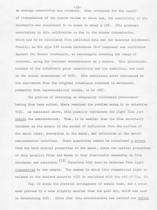
The problem of obtaining an adequately calibrated photosensor
having thus been solved, there remained the problem using it to determine
~(O). As mentioned above, this quantity represents the light flux just
inside the semiconductor. Thus, it is smaller than the flux externally
incident on the sample to the extent of reflection from the surface of
the metal layer, absorption in the metal, and reflection at the metal -semiconductor interface. These quantities cannot be calculated a priori from the bulk optical properties of the metal, since the optical properties
of thin metallic films are known to vary drastically depending on film thickness and substrate. (l5) Therefore
~(O)
must be inferred from light transmitted by the sample. The manner in which this transmitted light is related to the desired quantity <I>(O) is explained with the aid of fig. 10. [image:43.558.14.546.29.739.2]GOLD FRONT CONTACT
INCIDENT
BEAM
METAL MASK
cpl
'\
"""-.;
"
·.,'
"
"
·,,'
,,
cpo
-
---
,
BACK SURFACE
REFLECTION
~
Ga 2
o
3~T (TRANSMITTED BEAM)
PIGUIU: 10. Schematic representation of sample and beam geometry in photocurrent measurement, sh01~ing
various components of the incident beam.
I
w
-40-the back of the sample was aluminized). A portion of the beam from
the monochromator is passed by the metal mask; this portion, having a
;~
total photon flux . <P
1, is the beam incident on the sample. Some fraction
of this incident flux is transmitted to the semiconductor side of the
metal-semiconductor interface; this transmitted fraction <Ii , is the
0
flux sought. Some fraction of ~ , depending on absorption in the semi
-o
conductor, reaches the back surface; there, a further fraction is
reflected back into the semiconductor (subsequent reflections are
neglected) and the remainder emerges from the sample as the transmitted
flux, <PT.
The transmitted flux, <PT, and the incident flux, <P
1 can be
measured (the latter, with the sample removed). Their ratio is here
defined as f(I.),
At a wavelength at which sample absorption is negligible, the transmitted flux is simply related to the desired <Ii ,
0
Thus, at such a wavelength, we have
cp
=
0
(21)
(22)
(23)
Unfortunately f(I.) tends rapidly to zero as the wavelengths
of interest are approached, since at these wavelengths the sample is
strongly absorbing. (<P
1 can, of course, be measured at all relevant
*
Since the flux per unit area is of value only in a uniform beam,quantities representing total flux (and total sample current) will be
used hereafter. Thus, for example, <Ii will be discussed instead of
-41-wavelengths, and R can be calculated from the previously measured n(A)
or its extrapolation). The procedure adopted in this work has been to
extrapolate f(A) from the wavelength region in which it can be measured
into the region of interest, in which it cannot be measured. This procedure seems justifiable, since the refractive index of Ga
2
o
3 and the optical properties of Au (on which f(/.) presumably depends) co notvary strongly or discontinuously with wavelengths in this region.
The experimental values of f(;A.), and the extrapolation initially
made, are shown in fig. 11. When.this extrapolated f(t.), together with measurements of ~I and the total sample photocurrent I were used to calculate Q(/.), values of Q greater than one were found at very
short waveJ engths CA. <O. 25µn) for light polarized perpendicular to the
crystalline b-axis. Since the quantum efficiency for this structure
cannot theoretically be greater than one, this result suggests that
the calculated values of ~ are smaller than the actual flux. Whether
0
this error was due to an erroneous extrapolation of f(A) or a calibration
error in photocell sensitivity is unknown. However, since at these
short wavelengths the calculated quantum efficiency was virtually
independent of wavelength (that is,
Q
appeared to reach a limiting orsaturation value) and this value was calculated to be slightly greater
than one, it was assumed that the limiting value was actually the one
normally expected of
Q,
that isQ
=
1. This assumption yielded afurther calibration point on the f(A) curve; for we can write
1
Q
-
Iq~ 0
I (1-R)
Qf (/.)~I (24)
H'l ,,..._ >-' '-../ .025 .020
1
______-0
.015 ·
-/
.010!:::>"/
.22
/
/
• 23 / / / / .24 / / / / I .25 / ,../ , . / / / .26 / /
\~AVELENGTII (micrometers)
/
.27 0
~?
/ / 0
0
0
0 0 /
o/
. 0
0
TRANSMISSION 0
Q SATURATION 0
.28 .29
y
I ~ N I .30
-43-fig. 11, and a new "extrapolated" curve of f(.A) made to pass through it.
(As can be seen, the change was not large, amounting to about 30% at
short wavelengths). This final curve should yield ¢ to values accurate
0
to -
±
3% (the photocurrent measurement accuracy) at the short-wavelength.extreme, degrading more or less uniformly to the estimated accuracy of
the photon-flux m1easurement (-
±
15% at the long-wavelength extreme.)The values of Q calculated using this final f (I,) are shown in Flg.
12, for both polarizations. (The estimated accuracy of
Q
is the same asthat of¢ , discussed above). From these points corresponding values of
0
~can be calculated using equation (20). (The estimated accuracy of the
calculated value of a is discussed in Appendix C). These values of a
are plotted in fig. 13 (open circles). The filled circles are values
of a calculated from transmission, i.e. the same data as that displayed
in fig. 8;· except that different samples are not distinguished in
fig. 13. The agreement seen between a values calculated using the
two methods is substantial, particularly in the case of the
lower-energy edge, with polarization perpendicular to the b-axis. The
discrepancy in the case of the other polarization has not ?een
satisfactorily explained. Consideration of possible error sources
suggests that the values determined from transmission should be
[image:48.557.17.526.55.745.2]>-(_) :z: w ,_, (_) ,_, Ll.. Ll.. w
5
,_
I
r
5
02
0 0 0 0 0 0 0 0 0 0 0 - 44'-0 00 0
0 0
0
0
0
0
0
u
00
1
0
9
0 0 0 0 0 0 0 0
10-
3...L~-L~~~~-L...~~~~~
'
~~~~..1--~~~-...i~~~~_,J
4
.6
4
.
8
5
.
0
5.2
5.4
[image:49.557.10.544.14.724.2]PHOTON ENERGY
-46-IV. Conclusion
This thesis reports an experimental determination of the refractive
index and optical absorption coefficient of 8-Ga
2
o
3. The valuesdetermined for these constants are presented as functions of wavelength
in figures 5,6, and 13. The experimental techniques employed were
developed for the particular set of difficulties and opportunities
presented by the material properties of gallium oxide; however, since
a number of other materials share some of these properties, it is
expected that the techniques may prove useful to other investigators.
Because of the tendency of
8
-gallium oxide to cleave into thinplates with parallel faces, the conventional (prism) methods of
refractive index determination are not usable with it, but another
technique, exploiting interference due to multiple internal reflection
within the plates, was successfully used to determine the refractive
index over a wide range of wavelengths. This is the first application,
known to the author, of this technique over an extensive wavelength range,
particularly in the visible and ultraviolet spectral regions. The
technique has been shown to possess the property, not previously reported,
of revealing the existence of even a very slight birefringence in a
spectacular manner, and allowing its quantitative measurement without
the use of polarized light. A detailed analysis has been presented of
this application of interference to refractive index determination; the
technique should be of general utility in investigating the fairly
large class of materials that exhibit a strong tendency to cleave into
-47-Two experimental approaches were used in the measurement of
the absorption edge. For low values of a (a ~ 10 4 cm -1 ) the
conven-tional technique of measuring transmission of thin samples was used.
The application of this method for a > 104 requires the use of samples
of thickness of order lµm which are extremely difficult to prepare
and handle; for this reason, a new technique has been developed which
effectively utilizes an absorbing layer less than O.lµm thick. This
technique makes use of the fact that, for the fundamental absorption
edge of a semiconductor, each photon absorbed generates an electron-hole
pair. By collecting the carrier pairs generated in the thin depletion
region of a Schottky barrier, a photocurrent is obtained which can
be related to the absorption occurring in the same thin region. Using
this technique, the absorption coefficient measurement has been extended