International Journal of Innovative Technology and Exploring Engineering (IJITEE) ISSN: 2278-3075, Volume-8, Issue-11S2, September 2019
Abstract—Nowadays power consumption has the highest priority in designing high-performance electronics systems. The main purpose of this paper is to present a 16-bitKogge-Stone Adder where the low control operation is attained by the decrease of exchanging action. In this paper, we propose a method called Sense amplifier Lector based Half-Buffer (SALHB) by exemplifying Sense Amplifier Half Buffer (SAHB) with LECTOR algorithm to lessen leakage current in circuit structure. A 16-piece Kogge Stone Adder (KSA) is structured and actualized utilizing an asynchronous Quasi-Delay-Insensitive cell configuration approach known as the SALHB algorithm. Generally, SAHB is an asynchronous QDI configuration approach which applies 4-phase signaling protocol and sub-edge operation to obtain low control dissipation and rapid of operation. Additionally, LECTOR algorithm is applied to SAHB configuration approach through which leakage current can be decreased further to a great degree. A portion of the asynchronous QDI cell templates are Pre-charged Half-buffer(PCHB) and Autonomous signal validity Half-buffer(ASVHB), as both the templates, use completion detector circuits which lead to high power dissipation and large area overhead. SAHB design surpasses these drawbacks. But, SAHB has more leakage current. Hence, SALHB method was proposed to overcome the problem of high leakage current. In this paper, the performance of KSA is analyzed in terms of power, delay, energy, rise time, fall time, settle time, duty cyle, throughput and slew rate.
Keywords—Asynchronous, QDI, PVT, low power, SAHB, KSA, PCHB, ASVHB, LECTOR
I. INTRODUCTION
In VLSI, the design of CMOS circuits should focus on the important factor called power dissipation [1]. In battery -powered applications, the battery life will be reduced due to high control utilization and also affects its reliability, packaging, and cooling costs. There are three [2] most important parts of intensity dissipation: 1) capacitive power dissipation 2) cut off and 3) leakage current. The leakage current incorporates turn around bias diode flows and subthreshold flows [3, 4]. In CMOS circuits, the subthreshold leakage present and static power dissipation are increased with lessening of the limit voltage caused by voltage scaling [5].
Thusly, productive leakage control decrease systems are very crucial for the profound submicron [3] and nanometre circuits. In the proposed method, we embed two leakage control transistors (a p-type and a n-type) between draw up
Revised Manuscript Received on September 10, 2019. G Srikanth, CMR Technical Campus, India
Bhanu Murthy Bhaskar, Professor, Majmaah University, Riyaad, India
and pull-down system of the rationale gate in which the source terminal of one transistor controls the gate terminal of other leakage control transistor (LCT) [7]. Here, for any info combination, one of the LCTs is constantly "near its cut-off voltage". This significantly decreases the leakage flows with an increase in the resistance path from VDD to ground. Above all else, the gate-level netlist of the realized circuit is transformed into a static CMOS complex gate execution and after that LCTs are embedded to achieve a leakage-controlled circuit. The major characteristic of LECTOR [5,6,7] algorithm is in order to work effectively in both active and inactive states of the circuit, which results in improved leakage decrease in contrast to different procedures. Further, the proposed method SALHB defeats the cons shown by other QDI methods like PCHB [8,9], ASVHB[10] and SAHB[4] for leakage reduction.
Adders are widely used in microprocessors, DSPs and other high speed applications. One of the fastest parallel prefix adders [11,12] is Kogge-stone Adder[13,14] which generates carry faster[15] than other parallel prefix adders. This paper presents a 16-bit Kogge-stone adder incorporating an asynchronous QDI cell design approach known as SALHB which produce less power due to its sub-threshold operation and dynamic voltage scaling. It gives high speed of addition. The performance of the adder processor can be estimated by various metrics like power, delay, energy, rise time, fall time, settle time, duty cyle, throughput and slew rate.
This paper is organized as follows: Section 2 explains the existing asynchronous logic design techniques and its drawbacks. Section 3 describes the working principle of the proposed SALHB cell design approach. Section 4 presents the design of KSA with proposed SALHB. Results are depicted in section 5. Finally, Section 6 demonstrates the conclusion and future scope of the work.
II. EXISTING WORK
In modern VLSI design, the clock power of the chip is the main contributor for the total power dissipation. In order to save power and spurious pulses (glitches) Asynchronous circuits are highly essential. QDI templates are asynchronous circuit designs which are more robust to process fluctuations, temperature variations and FPGA remapping. Most popular QDI templates are:
Low Power Sub Threshold QDI Kogge Stone
Adder using Sense Amplifier Lector based Half
Buffer Cell Templates
2.1 Pre-Charged Half-Buffer (PCHB)
Pre-Charged Half-Buffer (PCHB) [8,9] chips away at domino rationale standard. Its configuration can manual for configuration fast circuits, regardless of whether yield stabilizers are always present however the structure of the basic cells are complicated because of its signal trustworthiness and dynamic rationale. Generally
[image:2.595.319.529.54.155.2], the realization approach is an integrated gate-level 4 phase pipeline dual-rail circuit realization. PCHB cell has a pull-up and pull-down structure, pull-down nMOS stack, 2 inverters and 2 weak feedback inverters at both sides of output. It has 2 handshake signals are named as Rack (acknowledge-in) and Lack (acknowledge-out) and “en” is an internal signal which is blended in a microcell. Q.T and Q.F represents self-complemented outputs. The architecture of PCHB cell template is shown in figure 1.
Figure 1: Architecture of PCHB cell template
The pre-charged half-buffer [8,9]structure consists of 2 completion detectors placed at both sides of the input and output. These both input completion detector (ICD) and output completion detectors (OCD) are used to validate the availability of input/ output. These both Input completion detector (ICD) and output completion detectors (OCD) are used to validate the availability of valid input/output. These completion detectors consist of a large number of gates which increases the power dissipation. Autonomous Signal Validity Half Buffer (ASVHB) is another QDI approach which has dominant performance than PCHB.
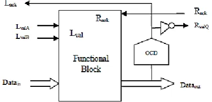
2.2 Autonomous Signal-Validity Half-Buffer (ASVHB) The realization of Autonomous signal-validity half-buffer (ASVHB)[10], the approach is an asynchronous-rationale quasi-delay inhumane (QDI) cell template for low power sub-edge operation (VDD = 0.2 V). Figure 2 delineates the layout of ASVHB cell format
Figure 2: Block diagram of ASVHB cell Template
The cell has a n-input information (n ≥ 1) all things considered meant as Data-In and yield information meant as Q. Data In and Q are in the dual rail encoding that requires two wires to encode a 1-piece datum. For instance, for the datum Q, there are a genuine wire (Q.T) and a false wire (Q.F). Both the genuine wire (Q.T) and the false wire (Q.F) are from the get-go '0' and amid the activity, one of the wires will be stated to '1' to demonstrate either a legitimate '0' or a substantial '1' information signal. The two wires can't be '1's all the while. The async handshaking signals are single-finished signs Lack (for example a perceive flag to the principal pipeline) and Rack (for example a perceive movement from the succeeding pipeline). For instance, the validity signals for Data-In of all the n information sources are LvalA and LvalB. The validity sign for Q is RvalQ. Although It operates under sub-threshold voltage, the structure of ASVHB [10] also has completion detector circuits at the output side, like PCHB [8,9] it dissipates more power due to the initial condition of operation and also because of the presence of a large number of gates in completion detector circuits. SAHB provides better functionality over ASVHB cell templates.
2.3 Sense Amplifier Half-buffer (SAHB)
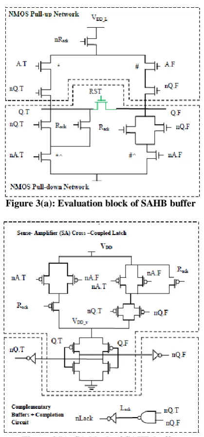
SAHB is a low control [4], rapid Asynchronous QDI cell format. The SAHB cell utilizes async 4-phase handshake protocol which has two alternate operation successions alluded to as evaluation and reset. It has two squares for obtaining a fast of operation and low control dissipation. Figure 3 demonstrates both the evaluation and SA square of buffer encapsulating SAHB cell.
In figure 3, A.T and A.F represents data inputs and the data yields are represented as Q.T/Q.F and nQ.T/nQ.F. The left channel handshake yields are indicated as Lack and nLack. Right-channel handshake signals are treated as inputs to the SAHB cell template and represented as Rack and nRack. The evaluation block is powered by VDD_L and the SA block by VDD respectively and their voltages may be the same or different. For the cell initialization, the nMOS transistor in green denoted with RST is exploited which is optional. As shown in figure 3, nRack acts as an evaluation flow control signal and the buffer logic function is realized by the nMOS pull-up network and expressed as in equation (1).
[image:2.595.62.281.251.479.2]International Journal of Innovative Technology and Exploring Engineering (IJITEE) ISSN: 2278-3075, Volume-8, Issue-11S2, September 2019
At first, every one of the sources of info reset to 0 and their correlative signs are set to 1. For instance, we initially think about A.F=1 (nA.F=0) in the evaluation stage, the nMOS pull-up system partially charges the voltage at Q.F to VDD_L and Q.T remains 0. As the substantial information is associated with the SA, cross-coupled latch turns on because of the immediate association of VDD_L to VDD and amplifies Q.F to 1. Thusly, Q.F is latched and nQ.F pushes toward getting to be 0. The dual rail result is validated by setting Lack to 1 (nLack =0). Amid the reset stage, the dual rail yield is unfilled as the vacant information (nA.T and nA.F are 1) is associated and Lack is gotten as 0. Now, the new evaluation of the SA block can be performed.
Figure 3(a): Evaluation block of SAHB buffer
Figure 3(b): SA block of SAHB buffer
Finally, both the evaluation block and SA block are firmly associated with each other to decrease the quantity of switching nodes, so it improves the speed and lessens the power dissemination. The performance of SAHB can be further improved by incorporating low power methodologies into the QDI templates.
III. PROPOSED METHOD: SENSE AMPLIFIER LECTOR HALF BUFFER (SALHB) TEMPLATES Asynchronous methodology is always dynamically appealing with synchronous as it offers high speed and low-power dissemination. The noteworthy exertion caused by synchronous framework plans are clock skew, control scattering, interfacing multifaceted nature and most pessimistic scenario performance. The SAHB cell entirely complies with the QDI conventions— gate without orphan with the isochronic fork supposition and info culmination. The rationale elements of the draw up system for AND/NAND is expressed as:
[image:3.595.65.275.215.665.2]Q.T = A.T · B.T (2) Q.F = A.F · B.F (3) Figure 4 shows the AND/NAND cell template in SAHB configuration.
Figure 4: Schematic of SAHB AND/NAND Cell evaluation block
[image:3.595.327.528.249.486.2]The circuit operation mainly depends on the input voltage levels. Figure 5 depicts the configuration of the circuit when A.F = VDD and B.F = 0.
[image:3.595.327.536.547.701.2]From figure 5, initially, assume that Q.F is reset at 0V, and then the inverter in the SA square will switch. The switching threshold voltage VX is expressed as
Where k = width of the pMOS over the nMOS transistor = the electron over hole saturation mobility. Now assume nRack= VDD, A.F= VDD, and nQ.F= VDD, as shown in Figure 5, the voltage at Q.F can be expressed a
VQ.F =
When valid input A is applied, then current I will charge Q.F even though another input is empty.
From equation 6, VQ.F should be less than switching threshold voltage to avoid the dual-rail output from being valid, if not too early operation of SAHB cell may take place which violates the transition sequences. By adjusting the threshold voltage shown in equation 4 to 6, there will be a less leakage power dissipation.
In the BSIM model (7), the threshold voltage is expressed as
where is the limit voltage, flat band voltage, is double the Fermi potential, k1 and k2 represent the nonuniform doping impact, and models the drain-instigated barrier bringing down (DIBL) impact, an undesirable punch-through current streaming between the source and drain underneath the surface of the channel. The leakage current for nMOS ransistors operating in the weak-reversal locale in SAHB is given by
Where, is the thermal voltage and is given by
is the subthreshold slope coefficient, and
An equation (8) presents a straightforward strategy for appraising the leakage current in a solitary NMOS transistor. Similarly, the expression for the leakage current in a solitary PMOS transistor can be obtained. Here, In proposed SALHB method, the gates are made up of arrangement parallel systems of PMOS and NMOS transistors. The leakage current provided by the MOS transistors coupled in parallel is the summation of the flows by the individual transistors. On the other hand, on the off chance that the transistors are associated in arrangement, at that point the evaluation of
leakage current will be complicated because of its nonlinear properties. Henceforth, stack of NMOS and PMOS gives low leakage current. LECTOR algorithm will make utilization of arrangement of stack transistors to control the leakage current.
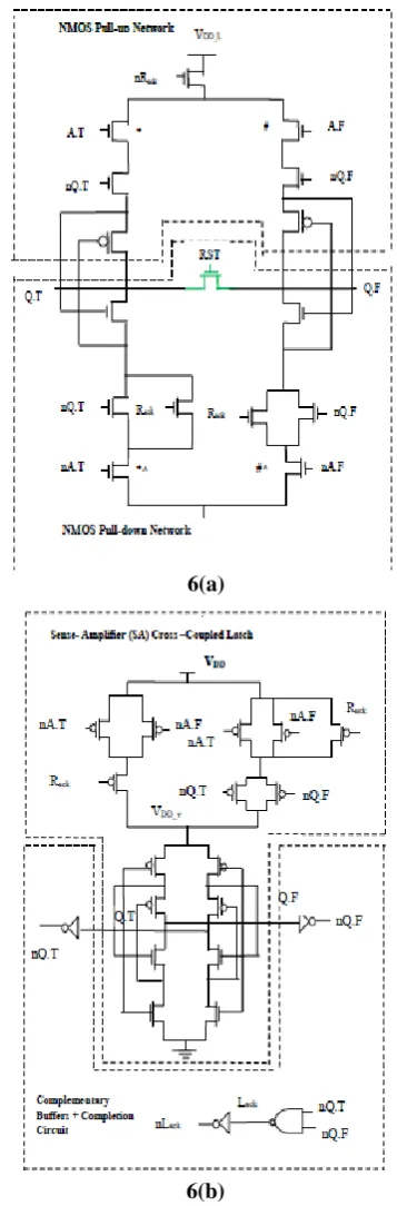
[image:4.595.339.518.173.716.2]SALHB utilizes LECTOR algorithm and hence ir is a low power, high-speed asynchronous QDI cell template. Figure 6 depicts both the evaluation and SA block of buffer cell of proposed SALHB cell design.
6(a)
6(b)
Figure 6(a): Evaluation block of a buffer cell (b) SA block of a buffer cell embodying SALHB powered by VDD.
[image:4.595.49.288.533.671.2]International Journal of Innovative Technology and Exploring Engineering (IJITEE) ISSN: 2278-3075, Volume-8, Issue-11S2, September 2019
SA block also has two LECTOR transistors placed at cross-coupled latch to reduce the leakage current in the circuit. For paradigm, we initially regard A.F=1 (nA.F=0) in the evaluation phase, the nMOS pull-up system moderately accuses the voltage at Q.F to VDD_L and Q.T ruins 0. since the persuading information is given to the SA square. The cross-coupled latch will move toward becoming on as a result of the straight association of VDD_L to VDD and amplifies Q.F to 1. Thus, Q.F is latched and nQ.F goes to 0. The dual-rail yield is valid by rising Lack to 1 (nLack =0). During the reset phase, the dual-rail yield is unfilled as the vacant info (nA.T and nA.F are 1) is applied and Lack is attained as 0. At this point, the new operation of the SA square can be performed. At last, both the evaluation square and SA square are firmly associated with each other to diminish the quantity of exchanging hubs, so it improves the speed and decreases the power dissipation. By structuring remaining rationale gates, for example, AND, AO, and XOR, we can design kogge-stone adder using this technique. Next section describes the design and implementation of 16-bit kogge-stone adder using SALHB technique.
IV. DESIGN OF 16-BIT KSA USING SALHB CELL DESIGN APPROACH
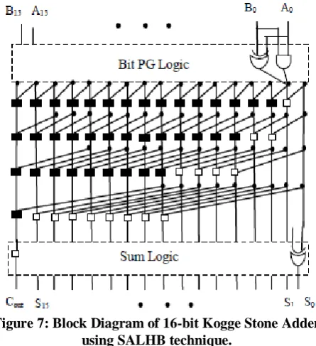
[image:5.595.323.529.314.720.2]This paper presents a 16 bit KSA [13,14] using an asynchronous QDI template known as SALHB technique which produce less leakage current[6] and high speed of operation.
Figure 7: Block Diagram of 16-bit Kogge Stone Adder using SALHB technique.
The equations of the Black cell and white cell in a Group PG logic of a SAHB Kogge-stone adder is given by
Figure 7 depicts the block diagram of 16 bit KSA. The primary input operands of the 16bit KSA are carry-in Cin A=A15 to A0, and B = B15 to B0. Whereas, the output operands are represented as S= S15 to S0 and carry-out Cout. Overall,
[image:5.595.58.281.400.644.2]six pipeline stages are required for structuring 16 piece KSA, brings about a forward latency of 6 pipeline delays and a throughput rate equal to one pipeline stage.
Figure 8: Circuit schematic and power dissipation of 16-bit kogge stone adder using SALHB an asynchronous
QDI cell design approach
Figure9. Simulation waveforms of 4bit KOGGE-STONE ADDER embodying SALHB cell
By using the equations (11) & (12) and figure 7, 16bit Kogge-stone adder was designed and implemented using an asynchronous QDI cell design approach called as SALHB technique to obtain less leakage current and high speed of operation. Figure 8 depicts the circuit schematic of 16-bit Kogge-stone adder using SALHB asynchronous QDI cell template. In the SALHB pipeline adder, the carry propagation time is shortened which leads to the high speed of operation. Next section demonstrates the simulation results of 16bit KSA using SAHB.
V. SIMULATION RESULTS AND DISCUSSION The design of Kogge-stone adder is done by using Mentor graphics EDA tool. The Kogge-Stone adder was simulated SALHB as shown in fig 9. SAHB suffers with leakage current, 16-bit Kogge-stone adder was designed using SALHB cell design approach which offers low power dissipation, high speed, and better performance. In this paper, the performance of KSA is analyzed in terms of power, delay, energy, rise time, fall time, settle time, duty cyle, throughput and slew rate.
5.1 Power dissipation
In a circuit, the power dissipation is defined as the conversion of source energy in the form of heat. The lifetime and reliability of the circuit decrease with an increase in power dissipation. Due to its minimizing switching activity, asynchronous logics have low power dissipation.
The average power dissipation of static CMOS circuit is given by
(13)
Where, Pavg is the total average power, PStatic is the static power dissipation; PDynamic is the dynamic power dissipation of the circuit.
5.2 Delay
In any circuit, Delay is characterized as the time required for the transmission of the yield voltage signal from the info voltage signal of a rationale gate.
5.3 Energy parameter
Vitality is characterized as the result of execution time and power utilization in the circuit. The performance of the circuit can be measured by utilizing the power-delay item. On the off chance that the obtained vitality is more that means all leakages are limited in the circuit. Energy parameter is given by
5.4 Rise time parameter
Rise time is the time occupied by a signal to change from an exact low value to a specified high value. These values are expressed as
(17)
Where, is the first derivative of the step response & is the delay time. Slow rise time results in significant power dissipation.
5.5 Fall time parameter
It is also called a pulse decay time. Fall time is the time occupied by the signal pulse amplitude to fall from an exact value. Fall time shrinks noise and glitches to produce the correct output.
5.6 Duty cycle
It is characterized as the time taken by a heartbeat signal to finish an OFF an ON cycle. Obligation cycle also characterizes whether the framework or gadget is in the active state in one cycle.
D = PW/T (18) Where, D is the obligation cycle,
PW is the beat active time or heartbeat width, and T is the total time of the signal
5.7 Throughput parameter
Throughput is defined as that how many transitions of a signal can take place in a given amount of time. It is also expressed as
Throughput rate = 1/T (19) Where, T is the total timeframe of a signal
5.8 Slew Rate parameter
Slew rate is characterized as the rate of change of yield voltage per unit time.
SR=max ( (20)
At high frequencies, slew rate will be high (i.e., quick response) as it directly proportional to frequency. It is given by
SR (21) Where f is the operating frequency & is the peak amplitude.
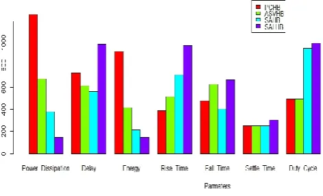
The Kogge-Stone adder was designed and implemented by using SAHB embodying LECTOR algorithm .Table I compares all the performance attributes of 16bit KSA using different asynchronous QDI techniques.
Table I: Performance evaluation of different asynchronous QDI logic16- bit KSA
Parameters PCHB ASVHB SAHB Proposed SALHB Power
Dissipation (n watts)
1261 675.9 378.4 148.3
Delay
(p sec) 733.14 614.59 563.16 991.9 Energy
( f Joules) 924.48 415.40 213.09 147.09 Rise time
International Journal of Innovative Technology and Exploring Engineering (IJITEE) ISSN: 2278-3075, Volume-8, Issue-11S2, September 2019
Fall time
(p sec) 477.27 627.96 402.99 668.4 Settle time
(n sec) 250.6 251.61 252.44 309.6 Duty cycle
(msec * Hz) 493.73 497.00 953.45 999.9 Throughput
(G Hz) 5 9.99 19.88 18.62
Slew rate
(G volt/sec) 1.65 2.77 3.19 3.02
[image:7.595.52.288.218.361.2]From Table I, it is clear that the Kogge Stone Adder with proposed QDI methodology provides low power.
Figure 9: Graph showing performance evaluation of SALHB
Although it gives little rise in delay, we attained energy savings. From our investigations, we found around 60% power savings and 30% energy savings compared to its predecessor. Figure 9 clearly shows that the proposed SALHB methodology is better one for power related metrics.
VI. CONCLUSIONS AND FUTURE SCOPE
In this paper, a 16 bit KSA is designed using various QDI cell templates. Low power technique called LECTOR is made use for the proposed SALHB asynchronous methodology to achieve better performance. By blending LECTOR algorithm, we achieved around 60% and 30% savings for power and energy respectively. In SALHB, the leakage power can be controlled to maximum extent with the introduction of lector transistors. On the other hand, with inclusion of extra transistors, delay has been raised up. Consequently rise time, fall time, settle time and duty cycle is also increased. If the adder chip is targeted for low power and energy the proposed methodology SALHB QDI template is the better alternative. The timing constraints may be improved with the help of high speed clock gating architectures.
REFERENCES
1. Bhattacharjee, P., Nath, B., & Majumder, A. (2018). LECTOR Based Clock Gating for Low Power Multi-Stage Flip Flop Applications. arXiv preprint arXiv:1805.07409..
2. Chandrakasan, A. P. and Brodersen, R. W. (1995), “Minimizing power consumption in digital CMOS circuits,” Proc. IEEE, vol. 83, pp.498–523.
3. Gu, R. X. and Elmasry, M. I. (1999), “Power dissipation analysis and optimization for deep submicron CMOS
digital circuits,” IEEE J. Solid-State Circuits, vol. 31, pp. 707–713.
4. Chong, K.S., Weng-Geng Ho, Lin, T., Gwee, B.H., and Chang, J.S. (2017), “Sense Amplifier Half-Buffer (SAHB): A Low-Power High-Performance Asynchronous Logic QDI Cell Template”, IEEE Transactions on VLSI Systems.
5. Narender, H. And Nagarajan, R.(2004),” LECTOR: A technique for leakage reduction in CMOS circuits”, IEEE Transactions on VLSI systems, Vol.12, No.2.
6. M. C. Johnson, D. Somasekhar, L. Y. Chiou, and K. Roy, "Leakage control with efficient use of transistor stacks in single threshold CMOS, "IEEE Trans. VLSI Syst., vol. 10, pp. 1–5, Feb. 2002.
7. S. Narendra, S. Borkar, V. De, D. Antoniadis, and A. P. Chandrakasan, “Scaling of stack effect and its application for leakage reduction,” Proc. IEEE ISLPLED, pp. 195–200, Aug. 2001.
8. Manisha, B. S., & Rudraswamy, S. B. (2018). VLSI Implementation of CMOS Full Adders with Low Leakage Power.
9. Chi-Chuan Chuang, Yi-Hsiang Lai1, and Jie-Hong R. Jiang(2014 ), "Synthesis of PCHB-WCHB Hybrid Quasi-Delay Insensitive Circuits” Department of Electrical Engineering, National Taiwan University, Taipei, 10617, Taiwan Computer Science Laboratory, Russia San Francisco, CA, USA.
10. Weng-Geng Ho, Chong, K.S., Bah-Hwee Gwee, Joseph Sylvester Chang(2014) ”Low power sub-threshold asynchronous quasi-delay-insensitive 32-bit arithmetic and logic unit based on autonomous signal-validity half-buffer” IET Circuits Devices system, Volume 9, Issue 4, pp.309-318, ISSN 1751-858X.
11. Manjunatha Naik. V, Poornima. N (2015),” Performance Analysis of Parallel Prefix Adder, International Journal of Electrical, Electronics and Data Communication”, ISSN: 2320-2084, Volume-3, Issue-7.
12. Rajnish Dubey, Jitendra Jain (2015),” An Efficient Processing by using Kogge-Stone High-Speed Addition Technique", International Journal of Computer Applications (0975 – 8887) Volume 131 – No.1. 13. Stone, H. S., and Kogge .P.M. (1973), “A parallel
algorithm for the efficient solution of a general class of recurrence equations,” IEEE Transactions on Computers. 14. Athira, T.S, Divya.R, Karthik.M, Manikandan.A (2017), “Design of Kogge-Stone for Fast Addition”, International Journal of Industrial Electronics and Electrical Engineering, Volume-5, Issue-4, ISSN: 2347-6982. 15. Chen, Y.K. and Pai, Y.T. and (2004)," The Fastest Carry