This is a repository copy of
Vertical leakage mechanism in GaN on Si high electron
mobility transistor buffer layers
.
White Rose Research Online URL for this paper:
http://eprints.whiterose.ac.uk/134429/
Version: Published Version
Article:
Choi, F.S., Griffiths, J.T., Ren, C. et al. (7 more authors) (2018) Vertical leakage
mechanism in GaN on Si high electron mobility transistor buffer layers. Journal of Applied
Physics, 124 (5). 055702. ISSN 0021-8979
https://doi.org/10.1063/1.5027680
[email protected] https://eprints.whiterose.ac.uk/ Reuse
This article is distributed under the terms of the Creative Commons Attribution (CC BY) licence. This licence allows you to distribute, remix, tweak, and build upon the work, even commercially, as long as you credit the authors for the original work. More information and the full terms of the licence here:
https://creativecommons.org/licenses/
Takedown
If you consider content in White Rose Research Online to be in breach of UK law, please notify us by
Vertical leakage mechanism in GaN on Si high electron mobility transistor buffer layers
F. S. Choi, J. T. Griffiths, Chris Ren, K. B. Lee, Z. H. Zaidi, P. A. Houston, I. Guiney, C. J. Humphreys, R. A. Oliver, and D. J. Wallis
Citation: Journal of Applied Physics 124, 055702 (2018); doi: 10.1063/1.5027680 View online: https://doi.org/10.1063/1.5027680
View Table of Contents: http://aip.scitation.org/toc/jap/124/5
Published by the American Institute of Physics
Articles you may be interested in
Graphene and related two-dimensional materials: Structure-property relationships for electronics and optoelectronics
Applied Physics Reviews 4, 021306 (2017); 10.1063/1.4983646
Effects of surface plasma treatment on threshold voltage hysteresis and instability in metal-insulator-semiconductor (MIS) AlGaN/GaN heterostructure HEMTs
Journal of Applied Physics 123, 184503 (2018); 10.1063/1.5027822
Leakage mechanisms in GaN-on-GaN vertical pn diodes
Applied Physics Letters 112, 233501 (2018); 10.1063/1.5033436
Structural and electronic properties of a-edge dislocations along ⟨1-100⟩ in GaN
Journal of Applied Physics 123, 244301 (2018); 10.1063/1.5034198
Mechanism for the formation of nitrogen-filled voids after annealing of GaN on a sapphire substrate
Journal of Applied Physics 124, 045304 (2018); 10.1063/1.5039755
Electron spin resonance in a 2D system at a GaN/AlGaN heterojunction
Vertical leakage mechanism in GaN on Si high electron mobility transistor
buffer layers
F. S.Choi,1J. T.Griffiths,1ChrisRen,1K. B.Lee,2Z. H.Zaidi,2P. A.Houston,2I.Guiney,1 C. J.Humphreys,1R. A.Oliver,1and D. J.Wallis1,3
1
Department of Materials Science and Metallurgy, University of Cambridge, Cambridge CB3 0FS, United Kingdom
2
Department of Electronic and Electrical Engineering, University of Sheffield, Sheffield S1 3JD, United Kingdom
3
Centre for High Frequency Engineering, University of Cardiff, 5 The Parade, Newport Road, Cardiff CF24 3AA, United kingdom
(Received 5 March 2018; accepted 18 July 2018; published online 3 August 2018)
Control of leakage currents in the buffer layers of GaN based transistors on Si substrates is vital for the demonstration of high performance devices. Here, we show that the growth conditions during the metal organic chemical vapour deposition growth of the graded AlGaN strain relief layers (SRLs) can significantly influence the vertical leakage. Using scanning capacitance microscopy, secondary ion mass spectrometry, and transmission electron microscopy, we investigate the origins of leakage paths and show that they result from the preferential incorporation of oxygen impurities on the side wall facets of the inverted hexagonal pyramidal pits which can occur during the growth of the graded AlGaN SRL. We also show that when 2D growth of the AlGaN SRL is maintained a significant increase in the breakdown voltage can be achieved even in much thinner buffer layer structures. These results demonstrate the importance of controlling the morphology of the high electron mobility transistor buffer layer as even at a very low density the leakage paths identified would provide leakage paths in large area devices.VC 2018 Author(s). All article content, except where otherwise noted, is licensed under a Creative Commons Attribution (CC BY) license (http:// creativecommons.org/licenses/by/4.0/).https://doi.org/10.1063/1.5027680
I. INTRODUCTION
Over the last two decades, GaN-based high electron mobility transistors (HEMTs) have been attracting growing interest for power switching applications due to their supe-rior electrical characteristics including high breakdown vol-tages, low on-resistances, and fast switching.1,2 However, challenges such as current collapse and buffer breakdown still exist and restrict the device’s ultimate performance.3 Studies have shown that breakdown voltage can be limited by the vertical breakdown from the GaN channel to the sub-strate.4,5For GaN on Si power devices, a key requirement is that a high voltage must be maintained between the drain contact and the substrate. It is also undesirable to see a sig-nificant vertical current flow across the buffer layer as this will increase the losses in the device.
Several mechanisms have previously been proposed for the vertical breakdown of GaN based devices. These include a space-charge-limited conduction model based on time and temperature dependent transient back-gating measure-ments,6,7band-to-band tunneling, and Poole-Frenkel mecha-nisms when the electric field is above 10 MV/m based on activation energy analysis.8–11 Leakage associated with defects in the buffer layer, presumably along threading dislo-cations, has also been proposed.12
As grown, un-intentionally doped (UID) GaN and AlGaN layers typically have a low n-type background dop-ing. This is due to impurities such as silicon and oxygen and to a lesser extent intrinsic point defects such as nitrogen and
Ga-vacancies which result in non-intentional donor doping. One approach to reduce the conductivity of such layers is the use of carbon doping. Carbon predominately occupies the N lattice site introducing deep acceptor-like trap states and hence compensates the n-type background doping.13,14It has been demonstrated that carbon-doped GaN buffer layers can enhance the breakdown voltage of HEMTs.15–18 Studies have also shown that carbon doping of buffer layers can have significant impact on the dynamic on-resistance and dispersion in devices at high voltages.19–23 Since carbon is present in the metal organic precursors used for GaN/AlGaN metal organic chemical vapour deposition (MOCVD) growth, the carbon level in layers is strongly dependent on the growth conditions used. Higher carbon levels are often associated with lower growth temperatures and lower V-III ratios which are also known to result in 3D growth of layers. Morphology can have a significant effect on the device per-formances. For example, deep pits have been reported to cause the reduction of breakdown voltage.24 Besides, 3D growth can also impact the incorporation of non-intentional impurities, so it is important to control both the morphology and dopant levels. Therefore, a further understanding and development of GaN buffer layer and strain relief layer (SRL) growth is vital to control the conductivity in the vari-ous parts of the HEMT structure.
In this paper, we study the impact of the growth condi-tions for the strain relief layer (SRL) on vertical leakage in GaN HEMT device structures grown on p-type silicon sub-strates. We present data for two AlGaN/GaN HEMT
0021-8979/2018/124(5)/055702/7 124, 055702-1 VCAuthor(s) 2018.
structures grown on silicon substrates under conditions designed to modify the carbon incorporation into the graded AlGaN SRL. It is found that in addition to changing the car-bon level in the layers, the change in growth temperature has a strong impact on the morphology of the layer and hence the unintentional incorporation of impurities. Cross-sectional scanning capacitance microscopy (SCM) is applied to study the distribution of mobile carriers that result from these impu-rities. The impact that the morphology during growth has on the structure of the buffer layer is examined by plan view scanning transmission electron microscopy (STEM) coupled with energy-dispersive X-ray spectroscopy (EDX) analysis to give compositional information. This structural information about these layers is then used to explain the difference in the vertical leakage currents measured on two HEMT structures.
II. EXPERIMENTAL
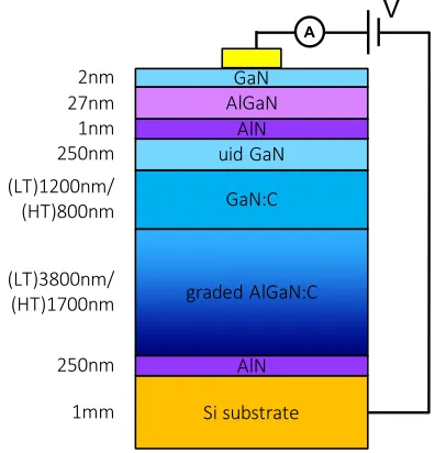
The HEMT structures used in this study were grown by metal organic chemical vapour deposition (MOCVD) in a 6-inch Aixtron close-coupled showerhead reactor. Trimethylgallium (TMG), trimethylaluminium (TMAl), and ammonia (NH3) were used as precursors, with hydrogen used as the carrier gas. The two samples studied have similar epitaxial structures as shown in Fig. 1 but with different layer thicknesses of the AlGaN:C SRL and GaN:C layers. The barrier layers in both samples are identical consisting of a GaN cap, AlGaN, AlN, and undoped GaN layers with a thickness of 2 nm, 27 nm, 1 nm, and 250 nm, respectively. In both samples, the buffer layers are comprised of carbon-doped GaN spacer layers and carbon-carbon-doped compositionally graded AlGaN SRL with AlN nucleation layers on silicon substrates. Graded AlGaN SRLs were used to relieve the stress due to the lattice and thermal mismatch between GaN and Si substrates. The Al ratio in the graded AlGaN layers decreased from 75% to 15% linearly along the growth direc-tion. For the low temperature (LT) sample, the temperature
was ramped linearly from 900C to 950C during growth of the AlGaN SRL, while the growth temperature was main-tained at 950C for the high temperature (HT) sample. The growth temperature of AlN and GaN:C for both samples is 1045C and 950C, respectively. The GaN spacer and the graded AlGaN layer in the LT sample are 1.2lm and
3.8lm, respectively, which are both thicker than that in the
HT sample with 800 nm and 1.7lm.
A range of experimental techniques were used to charac-terise the samples. During MOCVD growth, the reflectance of the epilayers was recorded using a 635 and 950 nm laser. The reflectance signal gives information about the thickness of the layer from the Fabry–Perot oscillations and also the roughness of the growing layer surface from the overall mag-nitude of the reflectance. The configuration used for the ver-tical leakage current measurement is shown in the schematic in Fig. 1. The vertical leakage current of the samples was measured using a Keithley source-measurement unit on alloyed (at 830C) Ti/Al/Ni/Au (20/120/20/45 nm) ohmic contacts fabricated on 100100lm2mesa etched structures
with an etch depth of 350 nm. Scanning capacitance micros-copy (SCM) is an electrical atomic force microsmicros-copy (AFM) technique. It allows simultaneous measurement of topogra-phy and electrical properties immediately below the sample surface. SCM utilizes a biased AFM tip to create a region depleted of carriers. The change of capacitance of the depleted region bias depends on the relative density and polarity of the mobile carriers.25,26 The measurements are taken using 90 kHz alternating bias and a 900 MHz capaci-tance sensor. SCM was operated in an open-loop contact mode with an AC bias of 5 V using a Veeco Dimension V AFM coupled with a SCM module and a Bruker SCM-PIC tip. Cross-sectional samples were prepared from both the LT and HT samples by cleaving alongf1120gafter marking the samples with a diamond scribe. Scanning transmission elec-tron microscopy (STEM) was used to study the morphology of the structures of the SRL. Energy-dispersive X-ray spec-troscopy (EDX) is a complementary technique of STEM to acquire the composition information by detecting the emitted characteristic X-ray from an atom bombarded by the electron beam. A FEI Tecnai Osiris microscope coupled with a FEI Super-X EDX system was used for this experiment. The plan view STEM samples were prepared using a FEI Helios focused ion beam (FIB) instrument.
III. RESULTS AND DISCUSSION
A. Vertical leakage
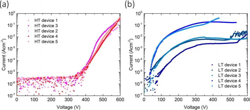
The leakage current values were acquired over 5 devices for each sample and the results are shown in Fig. 2. It is found that the LT sample exhibits high and very variable vertical leakage currents that exceed 1 mA cm 2 at 100 V, while the vertical leakage currents of the HT sample are con-sistent and less than 0.1 mA cm 2up to 430 V.
B. In-situmonitoring of growth
[image:4.612.74.272.525.731.2]Figure3shows the variation in measured 630 nm reflec-tance versus growth time during growth of the AlN, graded FIG. 1. Epitaxial structures of the LT and HT GaN-on-Si HEMT devices.
The LT sample has a thicker GaN buffer layer and AlGaN:C SRL than the HT sample.
AlGaN, and GaN layers for the two samples. Both samples have approximately the same peak reflectance when the growth of the AlGaN SRL is started. However, as the growth of the AlGaN SRL in the LT sample progresses, the value of the peak reflectance is reduced to less than half of its initial level indicating that the surface of the layer is becoming rougher. The peak reflectance then recovers as the Al frac-tion in the layer is reduced and the temperature increases. This is due to increased diffusion of surface atoms allowing the layers to smoothen. This clearly indicates that the LT layer goes through a phase of non-2D growth with a maxi-mum surface roughness in the middle of the AlGaN SRL. The surface then smoothens and recovers 2D growth again by the time the GaN:C layer was grown. In contrast, the reflectance signal of the HT layer is maintained at a higher level throughout the AlGaN SRL. The gradual damping of
the reflectance oscillations around a mean level for both the LT and HT samples is a result of development of a small, long range waviness at the epilayer surface which is common in nitride growths.27,28 The nm scale thickness differences result in small differences in the oscillation period at differ-ent points within the sampled area and therefore damping of the reflectance signals.
C. Scanning capacitance microscopy results
The surface AFM images with size 2020lm of the
[image:5.612.57.553.63.283.2]two samples are shown in Fig. 4. The root mean square of surface roughness is 1.08 nm and 1.05 nm for the LT and HT sample, respectively. The comparable surface morphology of the two samples suggests that the leakage pathway occurs through the cross-section of the structure. We therefore per-form cross-section SCM analysis. The SCM phase images show the net polarity of the mobile carriers. For the setup employed, the dark contrast represents n-type carriers. Insulating regions or regions with carrier densities lower than the detection limit of approximately 21017 carriers/ cm3will appear as noisy speckled patterns.29,30In Fig.5(a), FIG. 2. Vertical leakage current of the (a) HT sample and (b) LT sample with bias ramping from 0 V to 600 V. It can be seen that the vertical leakage currents in the LT sample are significantly higher and more variable than the HT sample.
[image:5.612.51.295.542.730.2]FIG. 3. 635 nm reflectance signal during growth for the LT and HT samples. The LT sample shows a significant decrease in the reflectance signal in the middle of the AlGaN SRL in contrast to the HT sample.
FIG. 4. AFM image of surfaces for (a) LT and (b) HT samples. The image size is 2020lm. The colour scale is 10 nm. The root mean square of
sur-face roughness Rqis (a) 1.08 nm and (b) 1.05 nm.
[image:5.612.315.560.610.731.2]a cross-sectional SCM phase image of the LT sample is shown. The many dark lobe-like features seen in the AlGaN SRL indicate regions of n-type conductivity. The contrast seems weak at the bottom of the lobes because the carrier density is close to the detection limit. These n-type regions represent conductive pathways which will decrease the volt-age that can be dropped across the buffer layers before breakdown occurs and therefore lead to high leakage cur-rents. In contrast, the HT sample does not show any of evi-dence of conducting regions in Fig. 5(b). According to the SCM, the doping level is below the detection limit of the technique. The silicon layer appears white in Fig.5(b)due to the p-type property of the material.
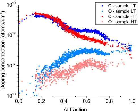
It should be noted that SCM measures the net mobile carriers in the sample rather than the number of dopant atoms and does not give any information about the dopant species. Secondary ion mass spectrometry (SIMS) was there-fore performed to provide information about the chemical dopant and impurity levels. Figure6shows carbon and oxy-gen doping concentrations in the AlGaN SRLs from the SIMS measurement. Since the AlGaN SRL thicknesses of two samples are different, the data are plotted against the Al fraction for easy comparison. The bottom half of the graded AlGaN layer of the LT sample shows a higher carbon level than the HT sample as expected due to the lower growth temperature. However, there is no obvious difference on the top of the graded AlGaN SRL when the growth temperature was ramped up. The carbon level is seen to increase gradu-ally as the Al fraction in the SRL reduces. For the oxygen
profiles, a gradual decrease in the oxygen is seen as the Al fraction is reduced. This is expected as the SIMS oxygen measurement background level is known to increase with the Al content of the layer. However, the oxygen level of the LT sample is consistently higher than that of the HT sample con-firming that oxygen is above the detection limit. The LT sample shows a peak in oxygen level in the middle of the AlGaN SRL which correlates with the maximum surface roughness from the reflectance traces. It should also be noted that the overall oxygen concentrations are much lower than the carbon concentrations in both samples. However, since the SIMS reading is an averaged value over a volume of material equivalent to the SIMS scan area (100lm2) by the
SIMS etch depth (a few nm’s), the actual local oxygen level could be much higher than that given in Fig.6if the oxygen concentration is laterally non-uniform as suggested by the conducting lobes seen in the SCM results. The carbon level of UID GaN and GaN:C for both samples is less than 1017 atoms/cm3 and mid 1018 atoms/cm3, respectively. The sili-con level in both samples is below the SIMS background detection limit throughout the structures.
D. Scanning transmission electron microscopy results
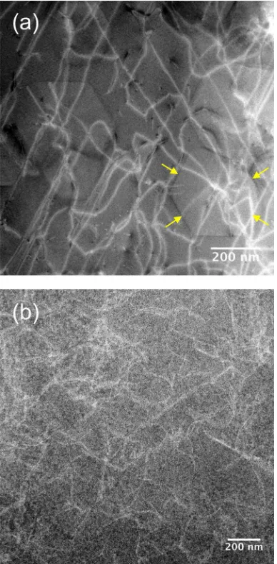
Plan view STEM samples were prepared by FIB from the middle of the SRL layers corresponding approximately to the position of the 50% Al fraction region in both the LT and HT samples. These plan view samples were then exam-ined in the STEM. Annular dark field images of two samples are shown in Fig. 7which clearly shows the misfit disloca-tion network in both samples. In addidisloca-tion, hexagonal features can be seen in two different regions of the LT sample as shown in Figs. 7(a) and 8(a), in which hexagons are about 400 nm across and have tangles of misfit dislocations at the centres. Such hexagonal defects are not found in the HT sample.
Energy-dispersive X-ray spectroscopy (EDX) analysis was carried out for a labeled hexagonal defect shown in Fig.
8(a)to provide compositional information. In Figs.8(b)and
8(c), it is shown that the hexagonal defect has a laterally graded composition that is Ga-rich and Al-deficient at its centre. This lateral variation in composition suggests that these hexagonal defects are formed from inverted hexagonal pyramidal pits, which are filled in as the compositionally graded AlGaN SRL is grown. The lateral variation in compo-sition results from growth on the semi-polar facets of the pits as the gas phase composition in the MOCVD reactor is changed to give the vertical grading of the SRL.
E. Origins of leakage pathways
[image:6.612.51.409.63.128.2]Given the above characterisation results, it is now possi-ble to deduce the origin of the conductive n-type features in FIG. 5. SCM phase images of the two samples in cross-section: (a) LT sam-ple and (b) HT samsam-ple. N-type lobe-like features are seen in the AlGaN SRL of the LT sample but not in the HT sample.
FIG. 6. Carbon and oxygen concentrations vs Al fraction in the AlGaN SRL of the LT and HT samples from SIMS measurement. The LT sample (blue) shows a higher carbon level in the bottom half of SRL than the HT sample (red). The oxygen level in the LT sample is always higher than that in the HT sample.
[image:6.612.53.296.512.709.2]the LT sample. Despite the enhancement of carbon incorpo-ration, a lower growth temperature may lead to formation of an inverted hexagonal pyramidal V-pit and hence severe sur-face roughening as shown by the growth reflectance data. The side walls of these pits are composed of semi-polar
f1011gfacets where it has been shown that oxygen is prefer-entially incorporated to form shallow donors in GaN.31,32 This preferential incorporation of oxygen explains the increased oxygen concentration for the LT sample compared to the HT sample in the middle of the SRL. It also explains the presence of n-type features in SCM results as the cleaved surface intersects the remnants of these doped V-pits to give the lobes of conductivity. Although the SIMS data show that the oxygen concentration is lower than the carbon concentra-tion, the actual local oxygen level can be an order of magni-tude higher, considering the fact that the SIMS value is averaged over a bulk volume. It is important to note that although the V-pits will have a significant influence on the conductivity of the buffer layers they are not visible on the epilayer surface, as they become completely filled in as the
[image:7.612.78.272.63.458.2]growth continues as illustrated in Fig.9. Thus, they can give rise to the buried n-type materials which provide a conduc-tive pathway extending from the bottom to the top of the graded AlGaN SRL and leave no evidence at the epilayer surface. Although there is a difference in the SRL and buffer layer thickness of the two structures, the fact that the thinner structure, with 2D growth, gives a considerably high break-down voltage strongly supports the conclusion that the conduction induced by 3D growth is the dominant leakage mechanism in the thicker structure. This confirms the FIG. 7. Annular dark field STEM images of the (a) LT sample and (b) HT
[image:7.612.334.534.63.574.2]sample. Hexagonal defects were only found in the LT sample but not the HT sample. A defect labeled with yellow arrows has misfit dislocations cluster-ing at the centre.
FIG. 8. A hexagonal defect in the middle of AlGaN SRL of the LT sample with (a) annular dark field STEM image (b) Ga and (c) Al composition images from EDX analysis. The composition images show that the defect is Ga-rich and Al-deficient at its centre.
importance of controlling the morphology during growth of thicker layers as well as the carbon doping level to reduce the vertical leakage in device buffer layers.
IV. CONCLUSION
The effect of modifying the MOCVD growth conditions of the AlGaN strain relief layer in GaN-on-Si HEMT struc-tures has been investigated. This study shows that reducing the growth temperature, as typically done to incorporate more carbon into the buffer layers, results in the formation of inverted hexagonal pyramidal pits which are correlated with a significant increase in the magnitude and variability of the vertical leakage currents. SCM phase imaging shows that this leakage is due to regions of a high n-type conductiv-ity. This is consistent with the preferential incorporation of oxygen on the semi-polar f1011g facets in V-pits whose presence is confirmed by STEM. In comparison, a HEMT structure which maintained 2D growth throughout gives much lower and reproducible leakage even for thinner buffer layers. It is also noted that even for very low densities of pits, which may not be detectable in thein-situ reflectance data, a similar mechanism will apply and give rise to break-down pathways in the buffer layers. Thus, controlling the MOCVD growth conditions to achieve 2-dimensional growth during SRLs and buffer layers is important as the device area is scaled up for high power GaN-on-Si HEMTs.
ACKNOWLEDGMENTS
This work was funded by the Engineering and Physical Sciences Research Council under Grant Code Nos. EP/ K014471/1 and EP/N01202X/1 and the European Research Council under the European Community’s Seventh Framework Programme Grant Agreement No. 279361 (MACONS).
1
N. Ikeda, Y. Niiyama, H. Kambayashi, Y. Sato, T. Nomura, S. Kato, and S. Yoshida, “GaN power transistors on Si substrates for switching applications,”Proc. IEEE98(7), 1151–1161 (2010).
2
U. K. Mishra, P. Parikh, and Y. F. Wu, “AlGaN/GaN HEMTs—An over-view of device operation and applications,”Proc. IEEE90(6), 1022–1031
(2002).
3S. C. Binari, P. B. Klein, and T. E. Kazior, “Trapping effects in GaN and
SiC microwave FETs,”Proc. IEEE90(6), 1048–1058 (2002). 4
H. Umeda, A. Suzuki, Y. Anda, M. Ishida, T. Ueda, T. Tanaka, and D. Ueda, “Blocking-voltage boosting technology for GaN transistors by wid-ening depletion layer in Si substrates,” inTechnical Digest-International Electron Devices Meeting(IEDM, 2010).
5
B. Lu, E. L. Piner, and T. Palacios, “Breakdown mechanism in AlGaN/ GaN HEMTs on Si substrate,” inDevice Research Conference-Conference Digest, DRC(2010), pp. 193–194.
6
C. Zhou, Q. Jiang, S. Huang, and K. J. Chen, “Vertical leakage/breakdown mechanisms in AlGaN/GaN-on-Si structures,” in Proceedings of the International Symposium on Power Semiconductor Devices and ICs
(2012), pp. 245–248.
7
P. Moens, A. Banerjee, M. J. Uren, M. Meneghini, S. Karboyan, I. Chatterjee, P. Vanmeerbeek, M. Casar, C. Liu, A. Salih, E. Zanoni, G. Meneghesso, M. Kuball, and M. Tack, “Impact of buffer leakage on intrin-sic reliability of 650V AlGaN/GaN HEMTs,” in Technical Digest— International Electron Devices Meeting, IEDM (2015), Vol. 2016, pp. 35.2.1–35.2.4.
8M. J. Uren, M. Caesar, S. Karboyan, P. Moens, P. Vanmeerbeek, and M.
Kuball, “Electric field reduction in C-doped AlGaN/GaN on Si high elec-tron mobility transistors,” IEEE Electron Device Lett. 36(8), 826–828
(2015).
9F. A. Marino, D. Bisi, M. Meneghini, G. Verzellesi, E. Zanoni, M. Van
Hove, S. You, S. Decoutere, D. Marcon, S. Stoffels, N. Ronchi, and G. Meneghesso, “Analysis of off-state leakage mechanisms in GaN-based MIS-HEMTs: Experimental data and numerical simulation,”Solid State Electron.113, 9–14 (2015).
10
P. Srivastava, J. Das, R. P. Mertens, and G. Borghs, “Silicon substrate engineered high-voltage high-temperature GaN-DHFETs,” IEEE Trans. Electron Devices60(7), 2217–2223 (2013).
11A. P
erez-Tomas, A. Fontsere`, J. Llobet, M. Placidi, S. Rennesson, N. Baron, S. Chenot, J. C. Moreno, and Y. Cordier, “Analysis of the AlGaN/ GaN vertical bulk current on Si, sapphire, and free-standing GaN sub-strates,”J. Appl. Phys.113(17), 174501 (2013).
12M. J. Uren, M. C
€
asar, M. A. Gajda, and M. Kuball, “Buffer transport mechanisms in intentionally carbon doped GaN heterojunction field effect transistors,”Appl. Phys. Lett.104(26), 263505 (2014).
13C. G. Van de Walle and J. Neugebauer, “First-principles calculations for
defects and impurities: Applications to III-nitrides,”J. Appl. Phys.95(8), 3851–3879 (2004).
14
M. J. Uren, J. M€oreke, and M. Kuball, “Buffer design to minimize current collapse in GaN/AlGaN HFETs,”IEEE Trans. Electron Devices59(12), 3327–3333 (2012).
15
S. Kato, Y. Satoh, H. Sasaki, I. Masayuki, and S. Yoshida, “C-doped GaN buffer layers with high breakdown voltages for high-power operation AlGaN/GaN HFETs on 4-in Si substrates by MOVPE,”J. Cryst. Growth 298, 831–834 (2007).
16
S. A. Chevtchenko, E. Cho, F. Brunner, E. Bahat-Treidel, and J. W€urfl, “Off-state breakdown and dispersion optimization in AlGaN/GaN hetero-junction field-effect transistors utilizing carbon doped buffer,”Appl. Phys. Lett.100(22), 223502 (2012).
17
C. Poblenz, P. Waltereit, S. Rajan, S. Heikman, U. K. Mishra, and J. S. Speck, “Effect of carbon doping on buffer leakage in AlGaN/GaN high electron mobility transistors,”J. Vac. Sci. Technol., B22(3), 1145 (2004).
18
[image:8.612.88.260.63.342.2]H. Tang, J. B. Webb, J. A. Bardwell, S. Raymond, J. Salzman, and C. Uzan-Saguy, “Properties of carbon-doped GaN,”Appl. Phys. Lett.78(6), 757–759 (2001).
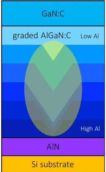
FIG. 9. Schematic diagram showing the evolution of the growth front of a V-pit opening up at the beginning of the AlGaN SRL growth, then closing up as the growth temperature is increased and the Al composition is decreased. Eventually, a planar surface is recovered at the end of AlGaN SRL growth. Preferential incorporation of oxygen on the semi-polar side-walls of the V-pit gives rise to the formation of a conductive pathway in the AlGaN SRL as indicated by the light green shaded area.
19M. J. Uren, M. Silvestri, M. Casar, G. A. M. Hurkx, J. A. Croon, J.
Sonsky, and M. Kuball, “Intentionally carbon-doped algan/gan HEMTs: Necessity for vertical leakage paths,” IEEE Electron Device Lett.35(3),
327–329 (2014).
20P. Moens, P. Vanmeerbeek, A. Banerjee, J. Guo, C. Liu, P. Coppens, A.
Salih, M. Tack, M. Caesar, M. J. Uren, M. Kuball, M. Meneghini, G. Meneghesso, and E. Zanoni, “On the impact of carbon-doping on the dynamic Ron and off-state leakage current of 650V GaN power devices,” inProceedings of the International Symposium on Power Semiconductor Devices and ICs(2015), Vol. 2015, pp. 37–40.
21
A. Pooth, M. J. Uren, M. C€asar, T. Martin, and M. Kuball, “Charge move-ment in a GaN-based hetero-structure field effect transistor structure with carbon doped buffer under applied substrate bias,”J. Appl. Phys.118(21), 215701 (2015).
22
I. Chatterjee, M. J. Uren, A. Pooth, S. Karboyan, S. Martin-Horcajo, M. Kuball, K. B. Lee, Z. Zaidi, P. A. Houston, D. J. Wallis, I. Guiney, and C. J. Humphreys, “Impact of buffer charge on the reliability of carbon doped AlGaN/GaN-on-Si HEMTs,” in IEEE International Reliability Physics Symposium Proceedings(2016), Vol. 2016, pp. 4A41–4A45.
23
M. R. Ramdani, M. Chmielowska, Y. Cordier, S. Chenot, and F. Semond, “Effect of carbon doping on crystal quality, electrical isolation and elec-tron trapping in GaN based structures grown silicon substrates,” Solid State Electron.75, 86–92 (2012).
24
S. L. Selvaraj, T. Suzue, and T. Egawa, “Influence of deep pits on the breakdown of metalorganic chemical vapor deposition grown AlGaN/GaN
high electron mobility transistors on silicon,”Appl. Phys. Express2(11), 111005 (2009).
25
C. C. Williams, “Two-dimensional dopant profiling by scanning capaci-tance microscopy,”Annu. Rev. Mater. Sci.29(1), 471–504 (1999). 26R. A. Oliver, “Advances in AFM for the electrical characterization of
semiconductors,”Rep. Prog. Phys.71(7), 76501 (2008).
27
A. Stafford, S. J. C. Irvine, Z. Bougrioua, K. Jacobs, I. Moerman, E. J. Thrush, and L. Considine, “Quantifying the smoothing of GaN epilayer growth by in situ laser interferometry,” J. Cryst. Growth 221(1–4), 142–148 (2000).
28
C. McAleese, OMVPE Growth and Characterisation of Nitride Semiconductor Materials(University of Cambridge, 2009).
29J. Sumner, R. A. Oliver, M. J. Kappers, and C. J. Humphreys,
“Assessment of the performance of scanning capacitance microscopy for n-type gallium nitride,”J. Vac. Sci. Technol., B26(2), 611 (2008). 30
J. Sumner, R. A. Oliver, M. J. Kappers, and C. J. Humphreys, “Scanning capacitance microscopy studies of unintentional doping in epitaxial lateral overgrowth GaN,”J. Appl. Phys.106(10), 104503 (2009).
31
S. C. Cruz, S. Keller, T. E. Mates, U. K. Mishra, and S. P. DenBaars, “Crystallographic orientation dependence of dopant and impurity incorpo-ration in GaN films grown by metalorganic chemical vapor deposition,” J. Cryst. Growth311(15), 3817–3823 (2009).
32
T. Zhu and R. A. Oliver, “Unintentional doping in GaN,” Phys. Chem. Chem. Phys.14(27), 9558–9573 (2012).