Int. J. Electrochem. Sci., 9 (2014) 3209 - 3221
International Journal of
ELECTROCHEMICAL
SCIENCE
www.electrochemsci.org
Study of
-rays Enhanced Changes of the ZnO:Al Thin Film
Structure and Optical Properties
Sarah M. Al-Sofiany1, H.E. Hassan1,2,*, A.H. Ashour3, M.M. Abd El-Raheem1,4
1
Physics Department, Faculty of Science, Taif University, Al-Hawiah, Taif, P.O. Box 888 Zip Code 21974, Saudi Arabia
2
Cyclotron Facility, Nuclear Research Center, Atomic Energy Authority, Cairo 13759, Egypt.
3
National Center for Radiation Research and Technology, Atomic Energy Authority, Nasr City, Cairo, Egypt
4
Department of Physics, Faculty of Science, Sohag University, Sohag 82524, Egypt
*
E-mail: hebrahim_hassan@yahoo.com
Received: 27 January 2014 / Accepted: 17 February 2014 / Published: 23 March 2014
In this work thin film samples of 300 nm thickness with composition ZnAlO were deposited on glass substrate by DC sputtering technique. The effect of the atmosphere gas contents during sputtering was studied by using Ar for some of the prepared samples and Ar+O2 mixture for the others. Additional
investigations were also done for the effect of the heat treatment of the samples for comparison with gamma irradiation. The samples were irradiated by three gradual gamma rays doses using 60Co source. The x-ray diffraction patterns showed that the deposited films were of amorphous structure and converted partially to crystalline form by irradiation. Optical properties of the investigated samples were measured using UV-vis spectrometer. The transmission spectra of irradiated samples were compared with that of unirradiated ones for comparison. In general, it was found that the optical parameters of the samples showed decrease in the transmittance after irradiation and the calculated optical energy gap was decreased. On the other hand, the heat treatment of the samples increased the energy gap. The data were analyzed and discussed in the light of gamma rays interaction with the investigated thin films.
Keywords: AZO thin film, DC sputtering, gamma irradiation, optical properties, TCO materials
1. INTRODUCTION
of Indium, Tin, Zinc and Cadmium as well as their doped elements which have been investigated by many groups around the world [8-9]. The ZnAlO was recently used instead of the conventional films like InSnO due to its high transmittance, non-toxicity, suitable resistivity, and low cost [3,4]. Zinc oxide is a II-VI compound semiconductor with optical band gap of 3.37 eV [10]. Its optical properties were efficient for using in several applications such as solar energy, electronic devices [11-17] sensors devices [18]. The properties of the thin film depend on the method of preparation and the treatment conditions like heating or using several surrounding atmospheres during preparation. Sputtering technique is simple and effective method to prepare different TCO materials in homogenous form and with variety of thicknesses (nm-µm) [19]. This technique allows using Ar gas or other type of gas mixture atmosphere during preparation which can change the crystal structure of the prepared film. It was reported that using O2 or H2 fractions during deposition of AlZnO could change the optical
transmittance and electrical resistivity [19-22]. Moreover, the wide verity of film thickness and heat treatment could change the microstructure, electrical and optical properties for the ZnO, Al-ZnO
[23,24].
In the recent years, modification of materials properties by irradiation gained much interest by several laboratories [25-27]. The effect of γ-irradiation on TeO and TeO2 thin films was reported
[25,26]. In this study physical properties were modified by irradiation with different doses of gamma rays for real-time dosimetry purpose [25]. .Furthermore, the effect of electron beam irradiation on
structural, optical, and electrical properties for Al doped ZnO with different O2 fraction have been
investigated [28]. Similarly, the effect of gamma radiation on the optical properties of Se90In10-xSnx
chalcogenide and thin films have been reported [29].
According to the above mentioned studies, it is noticed that little attention has been paid to comparison between irradiation effect and other conditional treatment on the optical conditions of AZO thin film. Therefore, we study in this work the enhanced changes occurred by using several conditions of preparation of ZnAlO thin film and compare these changes with that due to gamma irradiation. This may give added impetus on tuning the structural and optical properties of the AZO films. The results may help in development of the gamma rays dosimeteric tools by evaluating the relation between gamma doses and the tuned parameters of the investigated thin films.
2. EXPERIMENTAL
Thin film samples of composition ZnAlO were deposited on a glass substrate using UNIVEX 350 sputtering unit with dc power model TD20 and thickness monitor model INFICON AQM 160. The source target with composition ZnAlO (Al 20wt%, 99.9% purity) from Cathay Advanced Materials Limited, China. The glass substrates were first cleaned with acetone, rinsed in deionized water and then dried in inert atmosphere. Thereafter, the substrates were placed on the rotating holder of the DC sputtering unite. Two sets of the thin film samples were deposited by DC plasma discharge at room temperature using pure Ar (99.999%) and Ar:O2 (O2 2%) mixture gas. The power of the
obtained under deposition rate of 0.03 nm/s. After preparation, a group of the prepared samples were annealed at temperature of 500 oC for 2 hours in air.
Gamma-rays irradiation was carried out for all the investigated samples in a cavity of 60Co irradiator (medical sterilizer type CM-20) in the cyclotron facility, Nuclear Research Center of Egyptian Atomic Energy Authority with average dose rate of 1.4kGy/h. Three groups of the samples were exposed to three different doses: D1=201.6 kGy, D2=302.4 kGy and D3=470 kGy. Finally, the
[image:3.596.103.492.261.504.2]whole groups of the samples were assigned according to the preparation and irradiation conditions as given in table 1.
Table 1. Description of the investigated ZnO:Al samples according to treatment conditions.
Sample assignment Description
R-AR-D0 R-AR-D1 R-AR-D2 R-AR-D3
R: room temperature, AR: Ar gas (99.999%) D0: unirradiated, D1: dose1, D2: dose2, D3: dose3
H-AR-D0 H-AR-D1 H-AR-D2 H-AR-D3
H: heat treatment, AR: Ar gas (99.999%)
D0: unirradiated, D1: dose1, D2: dose2, D3: dose3
R-O-D0 R-O-D1 R-O-D2 R-O-D3
R: room temperature, O: (Ar: 98%, O2: 2%)
D0: unirradiated, D1: dose1, D2: dose2, D3: dose3
H-O-D0 H-O-D1 H-O-D2 H-O-D3
H: heat treatment, O: (Ar: 98%, O2: 2%)
D0: unirradiated, D1: dose1, D2: dose2, D3: dose3
The phase structural of the unirradiated and irradiated samples was analyzed using XRD diffractometer of type X’Pert Graphics employing Cu Kradiation (λ = 0.15405 nm). The optical properties were measured using a double beam UV-Vis spectrometers type JASCO-V-670 in the wave length range 200-1500 nm, where a blank glass substrate was used as a reference to eliminate the effect of the glass substrate over which the film was grown. Moreover, a blank glass substrate was also irradiated with the same dose of that corresponding to the investigated sample to be used as base line in the transmittance and absorbance measurement spectra.
3. RESULTS AND DISCUSSION
3.1. XRD spectra
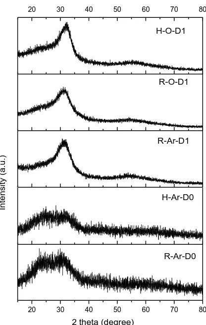
there are two humps around 25o and 30o, while the sample H-Ar-D0 showed broad hump. This broad hump of the unirradiated samples (R-AR-D0 and H-AR-D0) indicates the amorphous structure of the prepared film which reveals that heat treatment didn't improve the crystallinity of the prepared samples (Fig. 1-a,b). After irradiation, the spectra of the irradiated samples R-AR-D1, R-O-D1, O-D1, H-AR-D1 indicated that there was a tendency to crystallization around 33o as seen in Fig. 1. The gamma rays irradiation caused partial transformation from amorphous structure to crystalline phase, which is corresponding to the peak (002) of the AlZnO hexagonal Wurtzite structure [24]. On the other hand, there is no change in the spectra before irradiation for the samples that was prepared under mixed Ar+O atmosphere.
20 30 40 50 60 70 80
20 30 40 50 60 70 80
R-Ar-D0
2 theta (degree)
In
te
n
si
ty
(a
.u
.)
R-Ar-D1
[image:4.596.193.401.241.569.2]H-Ar-D0 R-O-D1 H-O-D1
Figure 1. x-ray spectra of the as-prepared and irradiated AZO thin films.
3.2 Optical properties 3.2.1 Transmission spectra
0 200 400 600 800 1000 1200 1400 0 10 20 30 40 50 60 70 80 90 100 T ra n s m it ta n c e ( % ) Wave length(nm) R-AR-D0 (a)
0 200 400 600 800 1000 1200 1400 0 10 20 30 40 50 60 70 80 90 100 Wave length(nm) H-AR-D0 R-AR-D1 H-AR-D1 R-AR-D2 H-AR-D2 R-AR-D3 H-AR-D3 (b)
Wavelength (nm) Wavelength (nm)
T ra n s m it ta n c e (% ) R-O-D0 (c)
0 200 400 600 800 1000 1200 1400 0 10 20 30 40 50 60 70 80 90 100 H-O-D0 (d)
0 200 400 600 800 1000 1200 1400 0 10 20 30 40 50 60 70 80 90 100 R-O-D1 H-O-D1 R-O-D2 H-O-D2
[image:5.596.102.481.89.582.2]R-O-D3 H-O-D3
Figure 2. UV spectra of the gamma irradiated AZO samples with different conditions of preparation: (a) as-deposited, (b) annealing, (c) as-deposited using Ar+O mixture during sputtering, (d) annealing after preparation using Ar+O mixture.
comparison with the unirradiated samples. The absorption edges for the treated samples didn't show any significant change from that of untreated samples whether by heating or irradiation or oxygen atmosphere.
3.2.2 Optical energy gap
The optical energy gap (Eg) value could be calculated using the formula:
αhν =C(hν-Eg)n , 1ln(1)
T d
(1)
where, the constant C is a parameter that depends on the transition probability and the constant n characterizes the direct (n=1/2) and indirect (n=2) allowed transition, α is the absorbance, T is transmittance and d is the film thickness. By considering the indirect transition (n=2), the (αhν)1/2 was plotted as a function of hν as shown in Fig. 3. The optical band gap Eg is determined by extrapolating
the linear portion of the obtained curves to zero absorption [32,33]. The determined value of Eg for the
as-deposited film in Argon atmosphere at room temperature (R-AR-D0) is 3.45 eV, which is close to that previously reported by Wang et al., (3.345 eV) [34,35]. Table 2 gives all the determined numerical values of the band gaps at different conditions of preparation and irradiation. Fig. 4-a,b represent the values given in Table 2 as a function of the absorbed dose. It is noticed that energy gap of the heated samples (H-Ar-D0, H-O-D0) is higher than that of the as-prepared ones (R-Ar-D0, R-O-D0). This could be explained through Burstein-Moss effect which describe the movement of Fermi level in the conduction band due to heating [24,36,37]. After irradiation with doses D1, D2 and D3 the band gap was decreased for all the samples prepared under the above mentioned conditions (Fig. 4a,b). The decrease percentages in every irradiation dose were amounted to 1.4-6.9 %. This could be attribute to formation of localized states due to structure defects. The increase of carriers localized states lead to decrease in the transition probabilities into the extended state, thus reduce the band gap as described in [38-40]. The following equation calculate the band gap widening (ΔEg) as a function of the carrier concentration (ne) in a degenerate semiconductor [41,42]:
3 / 2 3 / 2 2
8 ) / 3 (
e
g n
m h
E
(2)
Figure 3. Plots of (αhν)1/2 as a function of incident photon energy to determine the optical band gap at several conditions of preparations and irradiations.
Table 2. Changes in the numerical values of the band gap and charge density of the investigated samples with irradiation at different doses D1, D2 and D3.
D3 D2
D1 D0
Sample
ne(cm-3)
Eg(ev)
ne(cm-3)
Eg(ev)
ne(cm-3)
Eg(ev)
ne(cm-3)
Eg(ev)
5.72x1050
3.35
5.72x1050
3.35
2.02x1050
3.5 -
3.45 AZO-R-AR
2.96x1051
3.35
2.25x1051
3.4
2.25x1051
3.4
1.61x1051
3.65 AZO-H-AR
1.05x1051
3.4
1.05x1051
3.4
2.02x1050
3.5
5.72x1050
3.55 AZO-R-O
2.25x1051
3.35
1.61x1051
3.4
1.61x1051
3.4
1.05x1051
3.6 AZO-H-O
[image:8.596.84.551.431.731.2]
400 500 600 700 800 900 1000 1100 1200
R
ef
ra
ct
iv
e
in
d
ex
(
n
)
H-AR-D0
0 1 2 3 4
Wavelength (nm)
H-AR-D1 H-AR-D2 H-AR-D3
Figure 5. Curves of the refractive index as a function of wavelength for the AZO samples.
3.2.3 Refractive index
The refractive index can be obtained using the relation [45,46 ]:
R R n
1
1 (3)
where, R is the reflectance. Fig. 5 represents the obtained refractive index as a function of the wavelength (nm) which can be considered normal dispersion behavior. It is seen that after irradiation, the values of refractive index showed increments with a value 40 % at 400 nm and 6% at 1200 nm. This increase was observed for the heat treated samples that were irradiated by three doses D1, D2 and D3. This may be attributed to the crystal defects caused by irradiation which changed the color behavior of the films. Similar behavior was reported in a study on gamma irradiation of Fe-doped barium titanate thin films [47]. As an extended calculations for the optical parameters, we used Wample and Didomenico model [48,49] which is based on single oscillator formula to calculate the oscillator energy (E0) and dispersion energy (Ed). The formula could be written in the form:
2 1
2
) ( 1 )
1
( h
E E E E n
d o d
o
(4)
where, n is the refractive index and hν is the photon energy in eV. Plots of (n2
- 1)-1 versus (hν)2 for the heat treated sample, as an example, at irradiation doses D1, D2, and D3 are shown in Fig. 6 together with that of unirradiated one H-Ar-D0. From the slope (1/EdEo) and the y-axis intercept (Eo/Ed) the
values of Ed and Eo were determined for all the linear curves. The obtained values are given in Table3
and represented in Figs. 7a and b for comparison. It is noticed that by irradiation with the dose D1 the oscillator energy (E0) was decreased by a factor ~11% for all the samples (R-AR, H-AR, R-O, H-O)
localized after irradiation due to the crystal defects occurred by irradiation. From Fig. 7b it is noticed that the dispersion energy (Ed) was increased by irradiation with dose D1 for the samples H-AR, H-O
and R-O, and no further changes was observed for the doses D2 and D3 where Ed reached maximum
value. For the sample (R-AR) Ed showed significant increase at D3 in comparison with the other
samples. This changes reflects the degree of dispersion due to irradiation effects.
8.0 8.5 9.0 9.5
1/
(n
2 -1
)
H-AR-D0
0.0 0.2 0.4 0.6
(h)2 (eV)2
[image:10.596.150.436.179.395.2]H-AR-D1 H-AR-D2 H-AR-D3
Figure 6. Plots of (n2- 1)-1 versus (hν)2 for the heat treated sample.
0 50 100 150 200 250 300 350 400 450
20 25 30 35 40 45 50
R-AR
Ed
(
e
V
)
D (kGy)
R-O (b)
H-AR H- O
Figure 7. Variation of oscillation energy Eo (a) and desperation energy Ed (b) with increasing the
gamma irradiation dose.
0 50 100 150 200 250 300 350 400 450 4.0
4.4 4.8 5.2 5.6 6.0
R-AR
E0
(e
V
)
D (kGy)
R-O
(a) H-AR
[image:10.596.64.549.466.655.2]
Table 3. Changes in the values of the dispersion energy Ed and oscillator energy E0. D3 D2
D1 D0
Sample
Eo(ev)
Ed(ev)
Eo(ev)
Ed(ev)
Eo(ev)
Ed(ev)
Eo(ev)
Ed(ev)
4.85 45.21 4.61 32.68 4.62 32.29 5.22 27.75 R-AR 4.53 30.1 4.54 30.1 4.53 30.01 5.38 27.65 R-O 4.49 28.57 4.47 27.75 4.47 28.42 4.99 24.26 H-O 4.53 29.1 4.54 28.65 4.52 28.57 4.91 25.1 H-AR
3.2.4. Optical conductivity
The optical conductivity σop was calculated from the relation [45,50]: 4 c n
op (6)
where, c is the velocity of light, n is the refractive index, α is the absorption coefficient. The value of optical conductivity (σop) was plotted as a function of the photon energy as shown in Fig. 8. It is
noticed that the optical conductivity increases with increasing photon energy before and after irradiation for all the samples. The curves for the irradiated samples showed higher values of optical conductivity for the doses D1, D2 and D3 without any differences between the three doses effects. This confirms that the increasing of carries charges that was calculated in table 2 increases the optical conductivity of the samples by irradiation.
O p ti c a l c o n d c ti v it y ( s -1 ) H-AR-D0 H-AR-D1
1.0 1.5 2.0 2.5 3.0 3.5
0.0 5.0x10¹³ 1.0x10¹⁴ 1.5x10¹⁴ 2.0x10¹⁴ 2.5x10¹⁴ 3.0x10¹⁴ 3.5x10¹⁴ 4.0x10¹⁴ H-AR-D2
Photon energy (eV)
H-AR-D3
Figure 8. Optical conductivity as a function of the incident photon energy.
4. CONCLUSIONS
[image:11.596.151.412.431.631.2]
Thin film of ZnO:Al (Al: wt 20%) was prepared by DC sputtering technique and the XRD confirmed the amorphous state of the deposited film.
The crystallinity of the prepared films was changed by irradiation and heating.
The transmission properties were changed due to surface modification by irradiation and heating.
The optical band gap of the prepared films showed linear decrease with the irradiation doses which is useful in using the prepared films in dosimeter purposes.
Gamma irradiation causes changing in the optical parameters such as refractive index, oscillator energy and dispersion energy which may be useful in tuning these parameters by applying suitable absorbed dose.
Finally it can be noticed that the AZO thin films are highly sensitive to gamma irradiation which should be taken into consideration in the applied electronic industry.
References
1. Y. Liu, C. Hsieh, Y. Wu, Y. Wei, P. Lee, H. Hsieh and C. Liu, Appl. Surf. Sci., 282 (2013) 32. 2. R. Thangavel, M. Tariq, Y. Yia, C. Chang, C. Hsu, K. Yeh and M. Wu, J. Phys. Chem. Solids, 74
(2013) 1533.
3. F. Wang, C. Wang, J. Chen and Y. Yu, Mater. Let., 66 (2012) 270. 4. C.E. Kim and I. Yun, Appl. Phys. Lett., 100 (2012)13501.
5. C. Li, M. Furuta, T. Matsuda, T. Hiramatsu, H. Furuta and T. Hirao, Thin Solid Films, 517(2009) 3265.
6. H. Kong, P. Yang and J. Chu, J. Phys. Conf. Ser. 276 (2011) 012170.
7. S. Fernández, A. Martínez-Steele, J.J. Gandía and F.B. Naranjo, Thin Solid Films, 517 (2009) 3152. 8. K. Kato, H. Omoto, T. Tomioka and A. Takamatsu, Thin Solid Film, 520 (2011) 110.
9. R. Kumaravel, K. Ramamurthi, I. Sulania, K. Asokan, D. Kanjilal, D.K. Avasti and P.K. Kulria, Radiat. Phys. Chem., 80 (2011) 435.
10.Y. Moon, D. Moon, S. Lee and J. Park, Nucl. Inst. Meth. B, 268 (2010) 2522.
11.B. Nasr, S. Dasgupta, D. Wang, N. Mechau, R. Kruk and H. Hahn. J. Appl. Phys., 108 (2010) 103721.
12.Z.A. Wang, J.B. Chu, H.B. Zhu, Z. Sun, Y.W. Chen and S.M. Huang, Sol. St. Electr., 53 (2009) 1149.
13.W. Beyer, J. Hupkes and H. Stiebig, Thin Solid Films, 516 (2007)147.
14.D.C. Kim, B.H. Kong, S.K. Mohanta, H.K. Cho, J.H. Park and J.B. Yoo, Cryst. Growth Des. , 9 (2009) 4308.
15.J. Zhou, P. Fei, Y. Gao, Y. Gu, J. Liu, G. Bao and Z.L. Wang, Nano Lett., 8 (2008) 2725. 16.C. Guillen and J. Herrero, Appl. Surf. Sci., 282 (2013) 923.
17.C.H. Ahn, S.Y. Lee and H.K. Cho, Thin Solid Films, 545 (2013) 106 18.T. Ghosh and D. Basak, Sol. Energy, 96 (2013) 152.
19.W. Yang, S.M. Rossnagel and J. Joo, Vacuum, 86 (2012) 1452-1457.
20.J. Sung-Mok, K. Young-Hwan, K. Seong and Y. Sang-Im, Curr. Appl. Phys., 11 (2011) S191. 21.K. Kim, H. Choi, D. Cho, Y. Chung, K. Lee, N. Park and J. Kim, Thin Solid Films, 540 (2013) 142. 22. Q.J. Jiang, J.G. Lun, Y.L.Yuan, L.W. Sun, X. Wang, Z. Wen, Z.Z. Ye, D. Xiao, H.Z. Ge and Y.
Zhao, Mater. Lett., 106 (2013) 125.
23.J. Sengupta, R.K. Sahoo and C.D. Mukherjee, Mater. Lett., 83 (2012) 84-87.
24.F. Wang, M.Z. Wu, Y.Y. Wang, Y.M. Yu, X.M. Wu and L.J. Zhuge, Vacuum, 89 (2013) 127. 25.T.K. Maity, S.L. Sharma and G. Chourasiya, Radiation Measurements, 47(2012) 145.
27.A.M. Soleimanpour, Y. Hou and A.H. Jayatissa, Appl. Surf. Sci., 257 (2011) 5398. 28.E. Yun, J.W. Jung and B.C. Lee, J. Alloy. Compd., 496 (2010) 543.
29.A.A. Shaheen, M.M.A. Imran , O.A. Lafi, M.I. Awadallah and M.K. Abdullah, Radiat. Phys. Chem., 79 (2010) 923.
30.X.Y. Li, H.J. Li, Z.J. Wang, H. Xia, Z.Y. Xiong, J.X. Wang and B.C. Yang, Opt. Commun, 282 (2009) 247.
31.K.H. Kim, K.C. Park and D.Y. Ma, J. Appl. Phys., 81 (1997) 7764.
32.A.A.EL-Amin, A.M. Badr, F. Abdel-Wahab, Turk. J. Phys., 31 (2007) 331. 33.M. Jun and J. Koh, Nanoscale Res. Lett., 7 (2012) 294.
34.F. Wang, H.P. Chang, C. Tseng and C. Huang, Surf. Coat. Tech., 205 (2011) 5269. 35.C.E. Benouis, A. Sanchez-Juarez and M.S. Aida, J. appl. Sci., 7(2007) 220.
36.Y. Kim, W. Lee, D. Jung, J. Kim, S. Nam, H. Kim, Appl. Phys. Lett., 96 (2010) 171902.
37.S. Kim, Y. Moon, D. Moon, M. Hong, Y. Jeon and J. Park, J. Korean Phys. Soc., 49 (2006) 1256. 38.G..A.M. Amin, Nucl. Instr. Meth. B, 267 (2009) 3333.
39.H.S. Soliman, A.M.A. El-Barrya, S. Yaghmourb and T.S. Al-Solami, J. Alloy. Compd., 481 (2009) 390.
40.M.M. El-Nahass, K.F. Abd-El-Rahman, H.M. Zeyad and A.A.A. Darwish, Opt. Commun., 285 (2012) 2864.
41.A. Segura, J. A. Sans, D. Errandonea, D. Martinez-García and V. Fages, Appl. Phys. Lett., 88 (2006) 011910.
42.B.E. Sernelius, K.F. Berggren, Z.C. Jin, I. Hamburg and C.G. Granqvist, Phys. Rev. B, 37 (1988) 10244
43.L. Burs, J. Phys. Chem. , 90 (1986) 2555.
44.T. Supasai, S. Dangtip, P. Learngarunsri, N. Boonyopakorn, A. Wisitsoraat and S.K. Hodak, Appl. Surf. Sci., 256 (2010) 4462.
45.M.A. Mahdi, S.J. Kasem, J. J. Hassen, A.A. Swadi and S.K. J.A l-Ani, Int. J. Nanoelectronics and Materials, 2(2009) 163.
46.A. Abu EL-Fadl, A.S. Soltan and A.A. Abu-Sehly, J. Phys. Chem. Solids, 68 (2007) 1415. 47.O. Kongwut, A. Kornduangkeaw, N. Jangsawang and S.K. Hodak, Thin Solid Films, 518 (2010)
7407.
48.K.A. Aly, N. Afify, A.M. Abousehlly, A.M. Abd Elnaeim, J. Non-Cryst. Solids, 357 (2011) 2029–2034.
49.E. Márquez, J.M. González-Leal, A.M. Bernal-Oliva, R. JiménezGaray and T. Wagner, J. Non-Cryst. Solids, 354 (2008) 503.
50.J. I. Pankove, Optical Processes in Semiconductors, Prentice-Hall, New York (1971).