Rochester Institute of Technology
RIT Scholar Works
Theses Thesis/Dissertation Collections
1-1-2009
Interpixel capacitive coupling
Linpeng Cheng
Follow this and additional works at:http://scholarworks.rit.edu/theses
This Thesis is brought to you for free and open access by the Thesis/Dissertation Collections at RIT Scholar Works. It has been accepted for inclusion in Theses by an authorized administrator of RIT Scholar Works. For more information, please [email protected].
Recommended Citation
Interpixel Capacitive Coupling
by
Linpeng Cheng
B.S. Beijing Normal University, Beijing, China (1999)
M.S. Chinese Academy of Sciences, Beijing, China (2002)
A thesis submitted in partial fulfillment of the requirements for the degree of
Master of Science in the Chester F. Carlson Center for Imaging Science
Rochester Institute of Technology
January 2009
Signature of the Author
__________________________________________
Accepted by
__________________________________________________
Chester F. Carlson Center for Imaging Science
College of Science
Rochester Institute of Technology
Rochester, New York
Certificate of Approval
______________________________________________________
M.S. Degree Thesis
______________________________________________________
The M.S. Degree Thesis of Linpeng Cheng has been examined and approved
by the research committee as satisfactory for the thesis
requirements for the Master Degree in Imaging Science
_____________________________________ Dr. Stefi A. Baum, Thesis Advisor
_____________________________________ Dr. Donald F. Figer
_____________________________________ Dr. Zoran Ninkov
Thesis Release Permission Form
Chester F. Carlson Center for Imaging Science
College of Science
Rochester Institute of Technology
Rochester, New York
Title of Thesis: Interpixel Capacitive Coupling
I, Linpeng Cheng, hereby grant permission to the Wallace Memorial Library
of Rochester Institute of Technology to reproduce my thesis in whole or in
part. Any reproduction will not be for commercial use or for profit.
____________________________________________
Signature of the Author
____________________________________________
Interpixel Capacitive Coupling
Linpeng Cheng
A thesis submitted in partial fulfillment of the requirements for the degree of Master of Science in Imaging Science in the Center for Imaging Science, Rochester Institute of
Technology
Abstract
Interpixel coupling (IPC) is an electronic crosstalk where a pixel couples signal charges to its neighbors capacitively. It is a deterministic process, whereas diffusion crosstalk is stochastic. It will smooth normal image signal as well as Poisson noise. As a result, the conversion gain will be underestimated by the photon transfer method. However, the capacitive coupling has not received much attention until Andrew Moore and Gert Finger recently studied its potential effect on the measurement of responsive detective efficiency of image detector arrays in both theory and observation.
This thesis continues to investigate this electronic effect. The potential impact of capacitive coupling on the photometric measurement is first simulated. Methods based on inverse filer and Wiener filer are tested to correct this coupling impact. It appears that the signal loss can be restored to reasonable accuracy by applying the pseudo-inverse filter, provided that we have full knowledge of interpixel coupling.
Acknowledgements
My graduate study in Center for Imaging Science includes some of the most fun and valuable times in my life. I am very happy to the opportunity to learn imaging-related knowledge and skills with the help and encouragement of many people.
First, I would like to thank my advisors, Dr. Stefi Baum and Dr. Don Figer, for their careful guidance and inspiring advice. They envisioned a great research project, taught me the skills I needed to complete my M.S. degree. Thanks also go to my committee member, Dr. Zoran Ninkov, for his patient discussion and helpful suggestions in my research.
I would also like to thank my parents and girl friend for their care and support. I could not come to this point without their unselfish support materially and spiritually.
TABLE OF CONTENTS
1 Background ... 1
1.1 Monolithic CMOS array... 2
1.2 Hybrid CMOS array ... 5
1.3 Crosstalk ... 8
1.3.1 Optical crosstalk... 8
1.3.2 Diffusion ... 10
1.3.3 Interpixel capacitive coupling... 13
1.3.4 Basic mechanism of interpixel capacitance ... 18
2 Methodology on the measurement of interpixel coupling ... 24
2.1 Autocorrelation... 25
2.2 Optical spot illumination (Spotomatic) ... 26
2.3 Single pixel reset ... 28
2.4 F55 bombardment... 29
2.5 Reset bias Vreset... 30
2.6 Cosmic ray event (CRE)... 31
2.7 Hot pixels... 34
3 Impact of IPC on astronomical photometry... 36
3.1 Photometry in astronomy ... 36
3.2 Modeling IPC’s impact on photometry ... 39
3.3 Simulation of the impact of IPC on photometry ... 40
3.4 Simulation of the impact of IPC on SNR ... 46
3.5 Summary... 49
4 Interpixel coupling and read noise ... 51
4.1 Read noise ... 51
4.2 Modeling of read noise and IPC... 52
4.3 Autocorrelation of read noise ... 55
4.4 Summary... 65
5 Variations of interpixel capacitance ... 67
5.1 Capacitor and capacitance ... 68
5.2 Identification of cosmic ray events and hot pixels ... 72
5.3 IPC dependency on temperature... 74
5.3.1 Data analysis and results ... 74
5.3.2 Discussion ... 79
5.4 IPC dependency on single event intensity... 81
5.4.1 Overview... 81
5.4.2 Data analysis and results ... 82
5.4.3 Discussions... 87
5.5 IPC dependency on background... 90
5.5.1 Data analysis and results ... 90
5.5.2 Discussion ... 97
5.6 Summary... 98
6.1 Summary ... 100
6.2 Conclusions ... 101
6.3 Future research ... 103
Appendix A: Convolution and deconvolution ... 104
A.1 Linear shift-invariant system ... 104
A.2 Convolution... 106
A.3 Filtering theorem... 107
A.4 Deconvolution: inverse and Wiener filters ... 108
Appendix B: Sampling techniques in astronomical imaging...112
B.1 Correlated double sampling ...112
B.2 Fowler sampling...113
B.3 Up-the-ramp sampling ...114
LIST OF FIGURES
Figure 1.1 Left: cross section of a MOS capacitor (buried channel); right: p-n junction photodiode... 3
Figure 1.2 Architecture of monolithic CCD image sensors... 4
Figure 1.3 Sense node (photodetector) and the associated readout components in CMOS sensors. Left: photodiode (3T); right: Pinned photodiode or photogate (4T)... 4
Figure 1.4 Architecture of monolithic CMOS image sensor. ... 5
Figure 1.5 Cross section of typical IR hybrid CMOS detectors (per-pixel depleted) and Si multiplexer... 6
Figure 1.6 Cross section of Si-PIN detector array and associated the Si multiplexer. ... 8
Figure 1.7 A simple illustration of optical crosstalk occurring in image detectors. Photons incident on a target pixel finally may be absorbed in the neighbors due to inclined incident angle, multi-reflections, refraction in the image sensor, etc... 9
Figure 1.8 Illustration of diffusion crosstalk occurring in FSI image detectors. ... 11
Figure 1.9 Illustration of diffusion crosstalk occurring in BSI image detectors... 11
Figure 1.10 Absorption depth of photons in Si at different wavelengths. Absorption depth is defined as the distance where the incident radiation is reduced by 1/e (Bruggemann et al. 2002)... 12
Figure 1.11 Capacitive coupling in more typical per-pixel depleted detectors occurs in the space between the multiplexer and detectors between In bumps... 14
Figure 1.12 Major coupling in fully depleted detectors occurs in the detector bulk, in addition to the coupling in the space between the detectors and multiplexer. ... 15
Figure 1.13 Sketch of electric fields in detector arrays from top view (left: HgCdTe; right: Si-PIN). White area denotes regions with electric fields and is free of charge carriers. Shaded areas are p or n type regions of equal potential. Depletion regions in HgCdTe arrays are separated by conducting n-type detector bulk. The bulk of Si-PIN array is fully depleted with capacitive coupling between pixels inside the photodiode array. ... 15
Figure 1.14 Layout of detector nodes and interpixel capacitance. Photocurrent enters a detector node C0,0, which collects photocharges. The signal can still appear on adjacent nodes that are not exposed to photons (Moore et al. 2006). ... 20
Figure 2.1 A sample image of an optical spot projected onto the detector (left) and the surface plot of the pixel levels around the optical spot... 27
Figure 2.2 A portion of a frame illuminated by the Fe55 X-ray source with Al foil attenuation... 30
mode...32
Figure 2.4 Left: up-the-ramp samplings for a typical pixel hit by CRE (histogram mode); right: Pixels around the pixel hit by CRE in a difference frame...33
Figure 3.1 Illustration of aperture photometry for an astronomical object...37
Figure 3.2 Illustration of photometric image suffering from interpixel coupling...39
Figure 3.3 Workflow of the simulation process...41
Figure 3.4 Left: image of ideal airy pattern; right: image of re-sampled airy pattern with a size of 19×19 pixels (zoomed in). ...42
Figure 3.5 Comparison of signal change after the inverse and Wiener filters are applied. Relative signal change after deconvolution is referred to signal without IPC, i.e. F3 to F1_rd...43
Figure 3.6 Relative signal change in the aperture at different input signal levels after inverse filter was applied. Seven deconvolution kernels of different coupling amounts were tried at each input signal levels, including the true IPC. Relative signal change after deconvolution is referred to the signal w/o the IPC effect, i.e. F3 to F1_rd. See flowchart for descriptions...45
Figure 3.7 Comparison of SNR change after applying the inverse and Wiener filters. Relative SNR change after deconvolution is refered to signal w/o IPC, SNR3 to SNR1_rd. ...47
Figure 3.8 Relative SNR change at different signal levels after inverse filter was applied. Relative SNR change after deconvolution is refered to signal w/o IPC, SNR3 to SNR1_rd. ...49
Figure 4.1 Left: autocorrelation of an ideal Gaussian noise image with zero mean and σ = 5 DN; right: autocorrelation of same noise image but convolved with a low-pass filter...54
Figure 4.2 A mean-subtracted bias frame from the dark experiments of H2RG IR array at 37 K. The regions chosen are [140:500, 1070:1325], [520:1015, 1100:1380], [1025:1545, 1400:1680], and [1550:1980, 830:1180], as shown by the boxes...56
Figure 4.3 2-D autocorrelation of mean-subtracted bias, data taken from H2RG IR, regions of good uniformity used. Same dataset as in Figure 4.2. ...57
Figure 4.4 1-D autocorrelation of individual mean-subtracted columns. The resulting functions were averaged and scaled to 100 in the center. Test image data are from H2RG IR array. Same dataset as in Figure 4.2. ...58
Figure 4.5 1-D autocorrelation of individual mean-subtracted rows. The resulting functions were averaged and scaled to 100 in the center. Test image data are from H2RG IR array. Same dataset as in Figure 4.2...59
[2690:2815, 2535:2695], [3840:3970, 2720:2900], [3970:4095, 2720:2900], and [3460:3584, 2445:2660], as marked by the boxes. ... 61
Figure 4.7 2-D autocorrelation of mean-subtracted bias, data taken from H4RG SiPIN array, regions of good column bands used... 62
Figure 4.8 1-D autocorrelation of individual mean-subtracted columns. The resulting functions were averaged and scaled to 100 in the center. Test image data are from H4RG Si PIN array. ... 63
Figure 4.9 1-D autocorrelation of individual mean-subtracted rows. ... 64
Figure 5.1 Illustration of photodiode capacitance (C0) and interpixel capacitance (Cc) (Bai et al. 2007)... 68
Figure 5.2 Pixel node capacitance C0 and interpixel capacitance Cc. Only nearest neighbors are considered... 71
Figure 5.3 IPC variation with the detector temperature. Data taken at temperature ranging from 27.7K to 50 K. IPC is measured through cosmic ray events. ... 76
Figure 5.4 IPC variation with detector temperature. Data taken at temperature ranging from 27.7K to 50 K. IPC is measured via hot pixels. ... 78
Figure 5.5 IPC variation with the detector temperature, where measurements via CREs and hot pixels are put together. ... 79
Figure 5.6 IPC vs. CREs intensity, data taken at 37 K. IPC is measured by CREs... 83
Figure 5.7 IPC vs. CRE intensity, data taken at 37 K. IPC is measured by CREs. Same dataset used as in Figure 5.6. ... 85
Figure 5.8 IPC vs. hot pixel intensity, data taken at 37 K. IPC is measured by hot pixels. Same dataset used as in Figure 5.6. ... 86
Figure 5.9 IPC vs. event intensity, data taken at 37 K. The graph combines the data from CREs and hot pixels (in Figure 5.6 and Figure 5.8). Same dataset used as in Figure 5.6... 87
Figure 5.10 Depletion region for HgCdTe arrays. Left: before charge collection, right: after charge collection... 89
Figure 5.11 IPC (%) vs. CRE intensity (ADU) for different background labeled with different colors. ... 92
Figure 5.12 Mean IPC vs. background for different background levels. The IPC measurements were averaged from the same background. Background was determined from the flat field level. Same data as in Figure 5.11. ... 94
Figure 5.13 Mean IPC vs. difference between mean CRE and background for different background levels. The IPC measurements and CRE intensities were averaged for the same background. Same data as in Figure 5.11. ... 95
LIST OF TABLES
Table 3.1 Results of relative change of signal at different levels through inverse filtering. ... 45
Table 3.2 Results of relative change of signal at different levels through Wiener filtering. ... 46
Table 3.3 Results of relative change of SNR at different levels through inverse filtering. ... 47
Table 3.4 Results of relative change of SNR at different levels through Wiener filtering. ... 48
Table 4.1 Directories and test data for the test detector array H2RG HgCdTe. ... 55
Table 4.2 Column autocorrelation function with a 10-pixel shift in the -y and +y directions... 58
Table 4.3 Row autocorrelation function with a 10-pixel shift in the -x and +x directions. ... 60
Table 4.4 Directories and test data for the test detector array H4RG Si-PIN... 61
Table 4.5 Column autocorrelation function with a 10-pixel shift in the -y and +y directions... 63
Table 4.6 Column autocorrelation function with a 10-pixel shift in the -y and +y directions... 65
Table 5.1 Directory and test data for the test detector array H2RG HgCdTe. ... 76
Table 5.2 Results of IPC measurement at different temperature by CREs in the HgCdTe array... 76
Table 5.3 Results of capacitive coupling magnitude at different temperature estimated by hot pixels in the HgCdTe array... 77
Table 5.4 Results of capacitive coupling magnitude at different event intensities estimated by cosmic rays in the HgCdTe array... 84
Table 5.5 Results of capacitive coupling magnitude at different event intensities estimated by hot pixels in the HgCdTe array. ... 86
Table 5.6 Continued. ... 86
Table 5.7 Directories and test data for the test detector array H2RG HgCdTe. ... 91
Table 5.8 Results of capacitive coupling magnitude at different flat field levels estimated by cosmic rays in the HgCdTe array, data from BL1_J+PK50-2 photon transfer experiments. ... 93
1
Background
detectors and hybrid CMOS arrays, e.g. per-pixel depleted IR and fully depleted silicon PIN (Si-PIN) arrays.
1.1
Monolithic CMOS array
CMOS imaging devices use the conventional fabrication process for computer chips, as compared to the specialized techniques required for CCD fabrication. Therefore, the cost of CMOS sensors is significantly reduced. In addition, more on-chip elements can be integrated, reducing system size, complexity, and power consumption. These features make CMOS devices a promising alternative to replace CCD imagers.
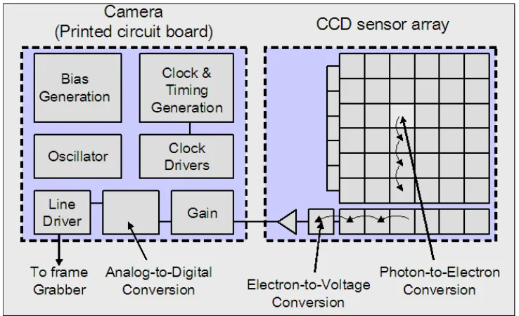
Most CMOS detectors are based on the p-n junction concept, where each p-n junction is a photodiode (photodetector), while CCD devices are referred to as voltage-induced p-n junctions because the applied gate voltage generates a potential well, causing the MOS capacitor (photogate) to behave like a p-n junction. In both imagers, incident photons striking the photoactive area of a detector array produce electron-hole pairs. For those pairs generated in the depletion region, they are then separated by the electric field there. Electrons and holes created outside the depletion region can diffuse into the depletion region, and these charge carriers also contribute to the collected signal. Besides the generic photodiodes, photogates and pinned-photodiodes also can be employed to sense photons in some CMOS sensors. The diagram in Figure 1.1 below illustrates the photo-sensing components in CCD and CMOS devices. Figure 1.2 shows the typical architecture of a CCD camera including readout and related functions.
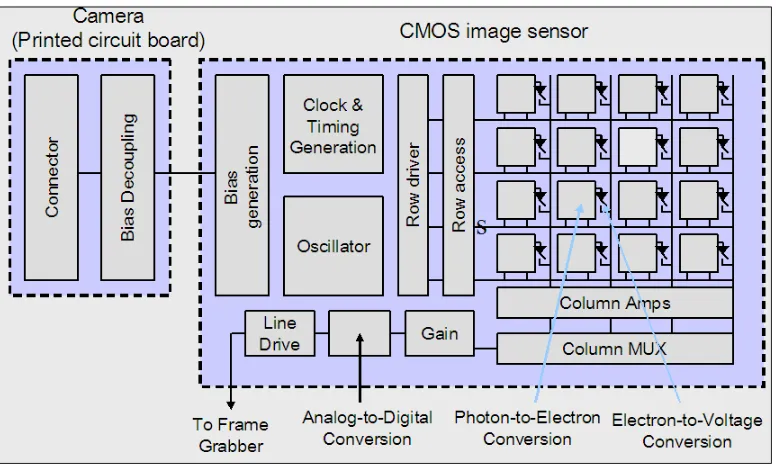
CMOS pixel. In the photodiode pixel, three Metal-oxide-semiconductor field effect transistors (MOSFET) are used to read out the charge on the diode: (a) a source follower MOSFET, which converts charge signal to an output voltage signal, (b) a reset MOSFET, which resets the photodiode and clear off the residual charges before an integration begins, and (c) a row-select MOSFET, which selects a row for scanned readout (Janesick 2004). This structure is the widely used 3T CMOS image sensors in consumer applications. In the photogate or pinned-photodiode pixel, in addition to the three MOSFETs described above, one more MOSFET is employed to transfer signal charge from the collection diode to the sense node, floating diffusion. This is widely referred to as the 4T structure. The diagrams below in Figure 1.3 show these two types of CMOS sensors. In some 4T CMOS image sensors, the pinned-photodiode is replaced by the photogate used in CCDs. Figure 1.4 presents the typical block diagram of CMOS image sensors.
Figure 1.2 Architecture of monolithic CCD image sensors.
Figure 1.4 Architecture of monolithic CMOS image sensor.
In a monolithic CMOS array, the photosensitive detector array and readout components for each pixel, e.g. the 3T or 4T structures in Figure 1.3, are built on the same piece of silicon wafer, as indicated in Figure 1.4. Therefore, monolithic imagers offer high integration, small volume, less power consumption, low cost, etc. However, the image quality of monolithic array is not good enough for astronomical applications, especially for space telescopes due to the design tradeoff between the pixel array and readout circuitry. Therefore, the system-on-chip imagers are only popular in consumer cameras.
1.2
Hybrid CMOS array
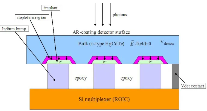
arrays. A hybrid sensor array is composed of two components: a detector array and readout integrated circuit (ROIC). The detector array is usually a photodiode array and responsible for photon-to-charge conversion. The ROIC is a multiplexer and functions as a charge-to-voltage converter and signal processor. Two components are built separately, and then precisely aligned and bonded together through indium bumps. Figure 1.5 illustrates the structure of a typical hybrid CMOS array. The unique feature of this hybrid is that both components can be optimized independently to maximize the detector sensitivity and ROIC functionality. Due to the extra fabrication steps required for interconnection components, this hybrid approach can cost much more than the monolithic counterparts, but the special design and structure make it potentially an ideal candidate for space applications.
Figure 1.5 Cross section of typical IR hybrid CMOS detectors (per-pixel depleted) and Si multiplexer.
InSb and HgCdTe, are competing in both ground and space-based astronomical applications.InSb is the simpler compound with the cutoff wavelength of 5.2μm and has been used for applications including the L and M band atmospheric windows (Finger and Beletic 2003). The alloy Hg(1-x)CdxTe allows to tune the cutoff wavelength to the specific application by varying the stoichiometric composition x (Long and Scmit 1970). This unique feature makes HgCdTe popular in the near-IR applications. In the IR detectors, the pixel array is typically per-pixel depleted. Both the two types of near-IR detectors employ the similar hybrid structure as shown in Figure 1.5.
Figure 1.6 Cross section of Si-PIN detector array and associated the Si multiplexer.
1.3
Crosstalk
Crosstalk is a phenomenon where photons strike a target pixel but the photo charges are collected by a different pixel. In typical imaging applications, signal electrons generated in a photo detector should remain in the target pixel. However, optical and electrical mechanisms can drive the charge carriers away such that they are collected by a neighboring pixel. The signal distortion causes modulation transfer function (MTF) loss, and thus damages the sensor sharpness. Crosstalk is highly unwanted in image applications. Generally there are three mechanisms causing crosstalk, i.e. optical, diffusion, and interpixel capacitance.
1.3.1
Optical crosstalk
However, just because an electron is released doesn't mean that it will be collected by the pixel well, it could be reabsorbed and recombine in the pixel or wander into adjacent pixels. When a photon intersects at an angle with a pixel surface, it is possible for that photon to enter the adjacent pixel's photodetector (photodiode) and not the photodetector under the incident surface. This will lead to contamination of the adjacent pixel's charge packet—called optical crosstalk. For instance, consider light going through a red filter area of a color filter array (CFA) at such an angle that it hits the photodetector under the adjacent green pixel. This will result in serious artifacts in the color image. As can be seen in Figure 1.7, optical crosstalk is dependent on the incident angle of light and pixel pitch. The larger the incident angle, the bigger the optical crosstalk.
Figure 1.7 A simple illustration of optical crosstalk occurring in image detectors. Photons incident on a target pixel finally may be absorbed in the neighbors due to inclined incident angle, multi-reflections, refraction in the image sensor, etc.
guide, etc (Hsu et al. 2004 and 2005). The metal shield method is more reliable than the black optical shields, but the metal is more costly, and takes up more space and adds weight.
1.3.2
Diffusion
Figure 1.8 Illustration of diffusion crosstalk occurring in FSI image detectors.
Figure 1.9Illustration of diffusion crosstalk occurring in BSI image detectors.
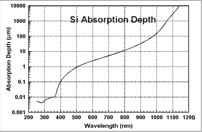
bulk. These electrons can wander into the wrong nearby pixel. Therefore, red light has higher diffusion crosstalk than the shorter blue and green light. In addition, as stated above, only those photoelectrons created outside the depletion region can cause diffusion, so pixels with a deeper depletion region will have less crosstalk effect. For instance, the Si-PIN detectors are fully-depleted pixels with electric fields throughout, and very few electrons can diffuse into neighboring pixels. Finally, diffusion crosstalk increases as pixel size is reduced as electrons only need to travel a short distance to adjacent pixels.
Figure 1.10 Absorption depth of photons in Si at different wavelengths. Absorption depth is defined as the distance where the incident radiation is reduced by 1/e (Bruggemann et al. 2002).
light. Diffusion problem can also be improved by using thinner epitaxial silicon at the expense of losing red sensitivity (Jansick 2003).
1.3.3
Interpixel capacitive coupling
CMOS array. However, the complicated layout of photodiodes and the associated readout components in monolithic array make this coupling negligible compared with optical and diffusion crosstalk. Therefore, the effect has not received much attention in the monolithic array. However, the unique interconnection structure in hybrid arrays provides the possibility for a capacitive coupling to be comparable to diffusion. The diagrams in Figure 1.11 and Figure 1.12 below illustrate how interpixel coupling could occur in the IR and Si-PIN arrays. As stated in Section 1.2, an IR array is a per-pixel depleted detector whereas the Si-PIN is a fully-depleted bulk detector. Both arrays can share the same multiplexer.
Figure 1.12 Major coupling in fully depleted detectors occurs in the detector bulk, in addition to the coupling in the space between the detectors and multiplexer.
Figure 1.13 Sketch of electric fields in detector arrays from top view (left: HgCdTe; right: Si-PIN). White area denotes regions with electric fields and is free of charge carriers. Shaded areas are p or n type regions of equal potential. Depletion regions in HgCdTe arrays are separated by conducting n-type detector bulk. The bulk of Si-PIN array is fully depleted with capacitive coupling between pixels inside the photodiode array.
coupling capacitance supposedly does not depend on these voltages. However, Bai et al. (2007) found that the magnitude of interpixel coupling is a function of detector bias, in the sense that the coupling amount decreases with increasing detector bias. This suggested that the mechanism of capacitive coupling is more complicated than we thought so far. A physical model based on detector material, bump interconnection, and multiplexer is greatly needed to explain capacitive coupling in more detail.
As described above, interpixel coupling and diffusion crosstalk have different mechanisms and thus different properties. Charge diffusion occurs during the charge collection and is dependent on the detector bias, temperature, and wavelengths of incoming light. On the other hand, capacitive coupling between pixels occurs after charge collection, and during the charge-to-voltage conversion process. This coupling strongly depends on the structure of readout circuits. In addition, diffusion is a stochastic process such that Poisson noise is completely uncorrelated to the adjacent pixels. Capacitive coupling is a fully deterministic process: Poisson noise measured with capacitive coupling is correlated to the neighbors (Moore et al. 2006). Therefore, given the full knowledge of capacitive coupling, its effect can be corrected through post-image processing.
should have appeared in the central pixel if there were not interpixel capacitance. The image quality is therefore distorted by the coupling. As presented above, interpixel coupling is a deterministic process whereas charge diffusion is a stochastic process. Poisson noise from diffusion crosstalk is not spatially correlated. However, Poisson noise with interpixel capacitance is spatially correlated, which causes the Poisson noise to be attenuated. In this regard, interpixel coupling behaves as a low-pass filter, which not only smooths the signal but the noise. Details will be presented in the next section.
Since the smoothing effect of capacitive coupling leads to underestimation of Poisson noise, conversion gain will be overestimated by the “noise squared vs. mean signal” method (Janesick 2001). This creates extra errors in the measurement of other sensor performance parameters, e.g. quantum efficiency (QE), dark current, and various noises, which strongly depend on the accurate measurement of conversion gain. As Moore et al. (2004, 2006) derived, a capacitive coupling of 1% to each adjacent pixel will result in an error of 8% in the measurement of noise square (variance), and thus an 8% error in the estimated conversion gain, as well as other related parameters.
1.3.4
Basic mechanism of interpixel capacitance
As Moore et al. (2004, 2006) stated, the detector element of an image detector array can be modeled as a capacitor C[i, j] = Cnode assuming the array is uniformly fabricated. Each capacitor receives a signal charge Q[i, j] over the integration time Δt. Modeling the array as a discrete linear shift-invariant (LSI) system, the output can be written as below:
= =−
−
=
M m N n cn
j
m
i
h
n
m
Q
j
i
V
0 0]
,
[
]
,
[
]
,
This can be simply rewritten as the convolution of Q[i, j] and hc[i, j], as shown below.
]
,
[
*
]
,
[
]
,
[
i
j
Q
i
j
h
i
j
V
=
c (1.2)where * denotes the 2-D convolution and hc[i, j] is the impulse response or point spread function of the detector array of size M×N. Ideally, there would be no crosstalk across the diode array and hc[i, j] would reduce simply to a discrete delta function:
node c
C
j
i
j
i
h
[
,
]
=
δ
[
,
]
(1.3)Thus the ideal output of the array is a voltage V[i, j] determined only by the signal charge collected locally. node
C
j
i
Q
j
i
V
[
,
]
=
[
,
]
(1.4)Due to capacitive coupling between pixels, the impulse response hc[i, j] is no longer a delta function, and the signal charges on each capacitor will redistribute inductively across the detector array. The final signal at a single detector node is dependent on not only the photocharge it collects, but the adjacent detector node and mutual coupling strength. Figure 1.14 shows the layout of the mutual capacitance Cc between detector nodes and note capacitance. Suppose a point light source striking a center pixel (detector node) and an amount of photocharge Qpoint is collected, whereas the neighbors have no photocharge. Due to capacitive coupling, a portion of center charge Qpoint will appear on adjacent detector
nodes by induction. The resulting charge distribution at each node can be
expressed as:
] , [
' i j
= ==
M i N jpo
Q
i
j
Q
0 0
'
int
[
,
]
(1.5)The impulse response of the array is thus
node po
c
Q
C
j
i
Q
j
i
h
int '[
,
]
]
,
[
=
(1.6)After normalizing the node capacitance, the impulse response becomes
int '
[
,
]
]
,
[
po ipcQ
j
i
Q
j
i
h
=
(1.7)Obviously, the summation of hipc[i,j] over all the detector nodes is
1
]
,
[
]
,
[
0 0 int
'
0 0
= = = ==
=
M i N j po M i Nj ipc
Q
j
i
Q
j
i
[image:35.612.153.450.349.639.2]h
(1.8)Figure 1.14 Layout of detector nodes and interpixel capacitance. Photocurrent enters a detector node C0,0, which collects photocharges. The signal can still appear on adjacent
Now interpixel coupling is modeled as a low-pass convolution kernel hipc[i, j], and a
real image can be expressed as the convolution of the initial signal Q[i, j] and the
coupling response, as indicated below.
] , [
' i j
Q ] , [ ] , [ * ]) , [ ] , [ ( ] , [ * ] , [ ] , [
' i j Qi j h i j M i j N i j h i j N i j
Q = ipc = + poisson ipc + rd (1.9)
where M[i, j], Npoisson[i, j], and Nrd[i, j] are the mean signal component, Poisson noise
(shot noise), and read noise, respectively. The difference of two images,
and , captured under identical conditions cancels out the mean signal component
and leaves only noise components, which are twice the variance of the original noises. ]
, [i j
D '[ , ]
1 i j Q
] , [
' 2 i j Q ] , [ ] , [ ] , [ * ]) , [ ] , [ ( ] , [ ] , [ ] ,
[ ' 1 2 1 2
2 '
1 i j Q i j N i j N i j h i j N i j N i j
Q j i
D = − = poisson − poisson ipc + rd − rd (1.10)
Assuming the images and are dominated by Poisson noise, the read
noise component in Eq. (1.10) can be negligible. It then becomes ]
, [
' 1 i j
Q '[, ]
2 i j Q ] , [ * ]) , [ ] , [ ( ] , [ ] , [ ] ,
[ ' 1 2
2 '
1 i j Q i j N i j N i j h i j
Q j i
D = − = poisson − poisson ipc (1.11)
From the Poisson distribution, the variance of a shot noise image in quanta is equivalent to the mean signal M. We have
]
,
[
]
,
[
2
i
j
M
i
j
poisson
N
=
σ
(1.12)The power spectral density of the difference image, SD(ξ,η), in Eq. (1.11) is
2
2
(
,
)
2
)
,
(
ξ
η
σ
N ipcξ
η
D
H
S
poisson
=
(1.13)where ξ and η represent the spatial frequency in the horizontal and vertical directions,
{
S
(
,
)
}
R
[
x
,
y
]
2
2h
[
x
,
y
]
*
h
[
x
,
y
]
FT
D D N ipc ipcpoisson
−
−
=
=
σ
η
ξ
(1.14)Where denotes the autocorrelation function of the difference image and is the
Fourier transform of power spectral density (Peebles 2000). As can be seen in Eq. (1.14), the autocorrelation of the difference image is equal to the correlation of the impulse response with itself, scaled by the Poisson noise square. As the impulse has a unit area, its autocorrelation also does. So the summation of Eq. (1.14) is
] , [x y RD 2 ,
2
]
,
[
poisson N j iD
i
j
R
=
σ
(1.15)Eq. (1.15) is very important for noise squared estimation because it is different form the conventional variance estimator, as shown below
mn
j
i
D
R
D i jNpoisson
=
=
, 2 2]
,
[
]
0
,
0
[
ˆ
ˆ
2
σ
(1.16)where the image size is m×n. Assuming that most capacitive coupling is to the four nearest neighbors, from Eq. (1.15), Moore et al. (2006) derived an approximate formula
to estimate Poisson noise variance 2 of a flat field scene,
poisson N σ
+
+
+
+
=
ji i j i j
N
D
i
j
D
i
j
D
i
j
D
i
j
D
i
j
mn
poisson
, , ,
2
2
[
,
]
2
[
,
]
[
1
,
]
2
[
,
]
[
,
1
]
2
1
ˆ
σ
(1.17)When the signal is weak enough that readout noise is not negligible, the power
spectral density SD(ξ,η) of the difference image D[i,j] becomes
2 2
2
(
,
)
2
2
)
,
(
rd poisson ipc N N
D
H
S
ξ
η
=
σ
ξ
η
+
σ
(1.18)Take the inverse Fourier transform of Eq. (1.18) and we obtain
{
S
(
,
)
}
R
[
x
,
y
]
2
2h
[
x
,
y
]
*
h
[
x
,
y
]
2
2[
x
,
y
]
FT
Dξ
η
=
D=
σ
Npoisson ipc ipc−
−
+
σ
rdδ
(1.19)where δ[x,y] is the Dirac delta function. The summation of Eq. (1.19) becomes
2 2 ,
2
2
]
,
[
poisson N rd j iD
i
j
R
−
σ
=
σ
(1.20)So Eq. 1.17 is replaced with Eq. 1.21 below
2
, , ,
2
2 [ , ] 2 [ , ] [ 1, ] 2 [, ] [ , 1] 2
2 1
ˆ rd
j
i i j i j
Npoisson mn D i j Di j D i j D i j D i j σ
σ −
+ + + +
=
(1.21)2
Methodology on the measurement of interpixel
coupling
2.1
Autocorrelation
As discussed in Sec. 1.3.4, the autocorrelation of the difference of two identically acquired flat field images is equal to the correlation of the impulse response
with itself. Therefore, by computing the autocorrelation function of the difference of two photon noise dominated images or any mean-subtracted photon noise dominated images, we can estimate an average coupling amount between adjacent pixels. Suppose the interpixel coupling magnitude in percentage to each of nearest neighbors is
] , [x y hipc
α .
Neglecting second-neighbor and diagonal neighbor coupling, the center pixel will have 1-4α of its original voltage signal, 4α appearing in the neighbors. The impulse response can be approximated as follows
] 1 , [ ] 1 , [ ] , 1 [ ] , 1 [ ] , [ ) 4 1 ( ] ,
[i j = − i j + i+ j + i− j + i j + + i j−
hipc
α
δ
αδ
αδ
αδ
αδ
(2.1)From Eq. (1.14) we get
2
2
]
,
[
]
,
[
*
]
,
[
poisson N D ipc ipcy
x
R
y
x
h
y
x
h
δ
=
−
−
(2.2)Neglecting the second-order terms, the correlation of with itself can be
approximated below.
In practice, we can normalize the autocorrelation function below, ] 0 , 1 [ 2 ] 1 , 0 [ 2 ] 0 , 0 [ ] 1 , 0 [ 2 1 ] , [ ] 1 , 0 [ 2 1 ˆ
, D D D
D y x D D R R R R y x R R + + ≈ =
α
(2.4)From Eq. (2.4), it can be seen that capacitive coupling is just half of the nearest-center terms in the normalized autocorrelation. In addition, the conventional Poisson noise estimator, as indicated in Eq. (1.16), will underestimate Poisson noise squared by 8α, and thus an 8α error in the conversion factor estimation by the photon transfer method. However, the autocorrelation method is sensitive to damage pixels, e.g. cosmic ray events and defective pixels, and outlying pixels. These special pixels need to be excluded from the difference image before implementing autocorrelation. The effectiveness of identification of these pixels will significantly affect the measurement accuracy. Either dividing the difference image into many small patches free of cosmic events and defects (Moore et al. 2006), or employing a mask to mask out those pixels (Brown et al. 2006) will make the computing of autocorrelation less efficient. What’s more, we need to capture a certain number of flat-field frames under exactly the same illumination conditions. This method is not used in this thesis to measure interpixel coupling.
2.2
Optical spot illumination (Spotomatic)
precisely before projecting the spot on a specific pixel. In addition, the spot positioning within the target pixel should be adjusted to near the pixel center, which can reduce the asymmetry of the crosstalk due to interpixel capacitance. A sample image under such optical spot illumination is displayed in Figure 2.1 below (Dorn et al. 2006). The coupling amount can be calculated by analyzing the pixel levels around the spot-targeted pixel. Figure 2.1 indicates how the shot image and surface plot of interpixel coupling PSF look. The big issue related to this method is that it requires high-quality instruments to generate an optical spot of tiny size and to position the spot precisely within a pixel. Another problem is charge diffusion and optical crosstalk. What is measured includes the crosstalk contributed not only from capacitive coupling, but also from diffusion and optical crosstalk. The measurement is the total of these three components, so this approach only gives us an upper limit upon the IPC magnitude. Practically, it poses extra requirements in the experiment to reduce the effects of diffusion and optical crosstalk, for instance, a specific wavelength of light can be used to minimize the diffusion effect.
2.3
Single pixel reset
pixel, will be the impulse response induced by capacitive coupling. A sample difference image will be similar to the one displayed in Figure 2.1. This will give us a good direct measurement of interpixel coupling, which is separated from charge diffusion and optical crosstalk as the coupling only occurs after the charge carriers are collected. However, the single pixel reset method is very sensitive to the readout speed. The video signal needs to be settled for sufficient time, which will reduce the residual signal. The experiments performed by Finger et al. (2006) show that the measured value of interpixel coupling was smaller in the fast readout direction than in the slow readout direction. This variation poses extra uncertainty on the IPC measurement.
2.4
F55 bombardment
A Fe55 source is widely used in the characterization of scientific image detectors, e.g. conversion gain and charge transfer efficiency in CCD (Howell 2000). Fe55 is a well-calibrated radioactive X-ray source. It emits a large amount of Kα photons with
energy of 5.9 keV (80%), and additional Kβ photons with energy of (20%). Impacting the
supposed to have only dark signal. Identifying the isolated single events and analyzing the pixel signal surrounding them, the coupling magnitude can be estimated in the same manner as the single pixel reset and spotomatic methods as stated in Sec. 2.2 and 2.3.
Figure 2.2 A portion of a frame illuminated by the Fe55 X-ray source with Al foil attenuation.
2.5
Reset bias
V
resetreset is characteristic of collecting signal charge. This mimic charge signal will redistribute around the center pixel by electric induction, and a portion will appear in adjacent pixels if capacitive coupling exists. Like the methods of signal pixel reset and optical spot illumination, the high voltage reset of single pixels also generates single isolated events that have strong signal. The signal in the neighbors gives us information on interpixel coupling. As we can see, one advantage of this approach is that it does not suffer from diffusion effect and optical crosstalk, because there is no photon strike and thus no photocharge generated. The measured crosstalk is all from capacitive coupling. However, this method is only applicable to the arrays with special readout modes, and implementing the experiment is complicated. Therefore, this is not a common method to measure IPC. So far, it is still in the test stage.
2.6
Cosmic ray event (CRE)
diffusion or capacitive coupling. In a similar fashion to the method dependent on single events, we estimate the coupling amount of neighboring pixels identifying isolated single cosmic ray events and analyzing the signal level in adjacent pixels.
In astronomical applications, the sampling up-the-ramp (UTR) is one of the widely-used sampling strategies, see Appendix B. It includes repeated sampling of the pixels. In this technique, the signal levels are read continuously for the entire integration time with the same interval, and then fit to a straight line. Cosmic ray events can be efficiently identified in the fitting process, see the details describing the procedure in Chap. 5. The identified independent cosmic events can be used to measure the IPC magnitude. For a typical pixel, its signal values in the sequence frames appear to form a straight line, as shown in Figure 2.3, where there are eight continuous samplings and the first sampling has been subtracted from each of the following samplings (same for other plots).
Figure 2.3 Right: Up-the-ramp readouts for a typical pixel (plus sign); right: histogram mode.
Figure 2.4 (left) shows the up-the-ramp sampling of a pixel hit by a typical cosmic event, where the pixel signal will jump to a very high level suddenly and keep almost unchanged over the integration. From the dramatic change of pixel level we can determine when the cosmic event hits the detector among the readout sequence. Subtracting the preceding frame from the frame where the cosmic event appears, we would obtain a distribution of pixel values around the pixel hit by the cosmic event, as shown in Figure 2.4 (left). The signals surrounding the central pixel can be used to estimate capacitive coupling. Note that the surface plot of a hot pixel and its surroundings appears not much different from a cosmic ray event, as indicated in Figure 2.4 (right). However, the plot of all the samplings in a hot pixel should look like that in Figure 2.3, except that the increment amount in the sequence is much bigger.
Figure 2.4 Left: up-the-ramp samplings for a typical pixel hit by CRE (histogram mode); right: Pixels around the pixel hit by CRE in a difference frame.
The procedure to measure the IPC is listed below:
increment in pixel levels and remove them.
3) Select non-isolated single cosmic events (events where their neighbors also are potential cosmic events). Keep only isolated single cosmic rays.
4) Calculate IPC magnitude using the pixels surrounding each isolated cosmic event. Take average for all the IPC estimates.
The detailed criteria to identify CREs and hot pixels are presented in Chap. 5. One concern for the CRE method is that the coupling amount includes not only interpixel coupling, but diffusion crosstalk. It therefore gives us an upper limit on the coupling magnitude due to interpixel capacitance.
2.7
Hot pixels
3
Impact of IPC on astronomical photometry
3.1
Photometry in astronomy
Astronomical photometry is a technique of measuring the flux, or intensity of an astronomical object’s electromagnetic radiation. Usually, photometry refers to measurement over a specific wavelength band of radiation, e.g. near IR, optical, etc; however, when both the amount of radiation and its spectral distribution are measured, it is termed spectrophotometry.
Photometry is conducted by collecting radiation from target objects by a telescope passing through some specialized filters, and then capturing and recording the light energy with a photosensitive instrument, e.g. photometers. Initially, photometry in the near IR through long-wavelength UV bands was done with a photoelectric photometer, an instrument that measured the light intensity of a single object by directing its light onto a photosensitive cell. In the visible spectral range, this technique has almost been replaced with modern digital cameras, e.g. CCD and CMOS imagers, which can simultaneously image multiple objects, though photoelectric photometers are still used in some special situations, such as where high time resolution is required (Sterken and Manfroid 1999, Romanishin 2002).
point spread function. This may be due to the point spread in the telescope optics, the detector array, astronomical seeing, etc. When measuring the total flux from a point source, we need to add up all the light from the object and subtract off the sky background. The simplest technique, adding up the pixel counts within a circle entered on the target object and subtracting off an average sky count, is known as aperture photometry, as illustrated in Figure 3.1. When doing photometric measurement in a very crowded field, such as in a globular cluster, where the profiles of stars overlap significantly, one must use deconvolution techniques, such as point spread function fitting, to determine the individual fluxes of the overlapping sources (Sterken 1999, Romanishin 2002).
Point source
aperture Point source
aperture
Figure 3.1 Illustration of aperture photometry for an astronomical object.
Relative photometry is the measurement of the apparent brightness of multiple objects relative to each other. Absolute photometry is the measurement of the apparent brightness of an object on a standard photometric system. These measurements should consistent with other absolute photometric measurements obtained with different telescopes or instruments. The absolute photometric measurement can be combined with the inverse-square law to estimate the luminosity of an object if its distance is known.
To get the total flux of a source, the missing flux outside the aperture needs to be corrected through calibration. Ideally, no flux is missing outside the specified aperture, and the aperture covers all the flux from a source. Several mechanisms can cause the flux spreading around a source, e.g. optical aberration, diffusion, interpixel coupling. If interpixel coupling exists, a portion of the total signal within a specified aperture will flow out into its neighbors, thus reducing the measured flux in the aperture. The measurement appears smaller than the real value. An extreme example is illustrated in Figure 3.2 below, where the aperture encloses only the central pixel, which encloses a point source, and the surrounding region is dark. When the image passes through a capacitive coupling, this causes a measurement error in the total signal within the aperture. The filter hipc[x,y] from interpixel coupling is written as follows:
100 1 1 2 1 2 88 2 1 2 1 ] , [ × = y x hipc
only 2%. In practical cases, the error should be smaller, but we should correct this uncertainty for precise photometric measurement.
Figure 3.2 Illustration of photometric image suffering from interpixel coupling.
3.2
Modeling IPC’s impact on photometry
The effect of interpixel coupling can be modeled as a convolution process as it is deterministic. Applying linear filtering theory, the IPC can simply be taken as another component of the total point spread function (PSF) of the detector array—a strong point
source will spread out somewhat. Assume the IPC component of PSF is and
the original signal image is where i and j denote the pixel position, the resulting
signal will be the convolution of with , ignoring the readout
noise.
] , [x y hipc
] , [i j f
] , [
' i j
f f[i,j] hipc[x,y]
]
,
[
*
]
,
[
]
,
[
'
i
j
f
i
j
h
i
j
f
=
ipc (3.1)
H
[
,
]
FT
1{
h
1
[
i
,
j
]
}
ipc
inv
ξ
η
=
− (3.2)measurement by applying an inverse filter Hinv[ξ,η] if the magnitude of interpixel
coupling is well known. However, when the image signal-to-noise ratio (SNR) is low and thus read noise is not negligible, the inverse filter may not be a good choice to
deconvolve the blurred image. Instead, a Wiener filter Hwiener[ξ,η]
f
is supposed to
restore the blurred image betteras it was derived by minimizing the total squared error of
the recovered image signal compared to the correct signal (Helstrom
1967). When the additive noise (read noise) is negligible, the Wiener filter reduces to the inverse filter as indicated in Eq. 3.4.
] , [
' i j
f [i, j]
]
,
[
]
,
[
*
]
,
[
]
,
[
'
i
j
f
i
j
h
i
j
N
i
j
f
=
ipc+
rd (3.3)[ ]
[ ]
[ ]
[ ]
[ ]
[ ]
[ ]
2 2 2 *,
,
,
,
,
,
,
,
η
ξ
η
ξ
η
ξ
η
ξ
η
ξ
η
ξ
η
ξ
F
N
H
H
H
rdwiener
Γ
=
Γ
+
=
(3.4)3.3
Simulation of the impact of IPC on photometry
stage is denoted as F3. We can see if the signal can be recovered to the stage before the smoothing effect due to interpixel coupling.
Figure 3.3 Workflow of the simulation process.
Figure 3.4 Left: image of ideal airy pattern; right: image of re-sampled airy pattern with a size of 19 19 pixels (zoomed in). ×
In the simulation, the re-sampled pattern was scaled such that the true signal F0 varied in the range from 4000 to 10 digital counts (ADU). We need to see how the deconvolved signal F3 changes with respect to the signal without IPC filtering F1_rd over these signal levels. Besides the true IPC h0, six error IPC kernels were tried in the
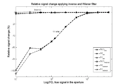
deconvolution. The error IPCs are chosen according to Eq. 3.5 below. Both inverse and Wiener filters were used to deconvolve the blurred image pattern. All the results are listed in Table 3.1 and Table 3.2. However, in Figure 3.5 only the results from deconvolution kernels h0, h0.5
, and
h
1 are presented.h
0inv and h0Wiener mean the true IPC magnitude isFigure 3.5 Comparison of signal change after the inverse and Wiener filters are applied. Relative signal change after deconvolution is referred to signal without IPC, i.e. F3 to F1_rd.
2
,
,
100
0 11 0 1 0 0 1 0 1
i
x
i
x
x
x
x
x
x
x
x
x
h
i=
=
=
(3.5)So , and
25 . 0 5 . 0 25 . 0 5 . 0 100 5 . 0 25 . 0 5 . 0 25 . 0 5 . 0 = h 5 . 0 1 5 . 0 1 100 1 5 . 0 1 5 . 0 1 = h
Throughout the simulation, the input IPC hipc stays unchanged, as shown below. The
gain of 1 e-/ADU).
0
3
.
1
0
5
.
1
100
5
.
1
0
3
.
1
0
0
=
=
h
h
ipcFigure 3.5 indicates that both filters work very well at high signal levels, however, the Wiener filter performs much worse than the inverse filter at low signal levels. Therefore, we just consider the inverse filter in our simulation presented in the following.
aperture small. This may explain this trend at low signal levels.
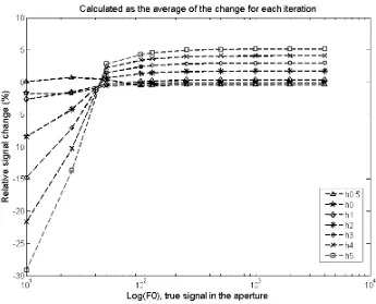
[image:60.612.137.482.119.398.2]Figure 3.6 Relative signal change in the aperture at different input signal levels after inverse filter was applied. Seven deconvolution kernels of different coupling amounts were tried at each input signal levels, including the true IPC. Relative signal change after deconvolution is referred to the signal w/o the IPC effect, i.e. F3 to F1_rd. See flowchart for descriptions.
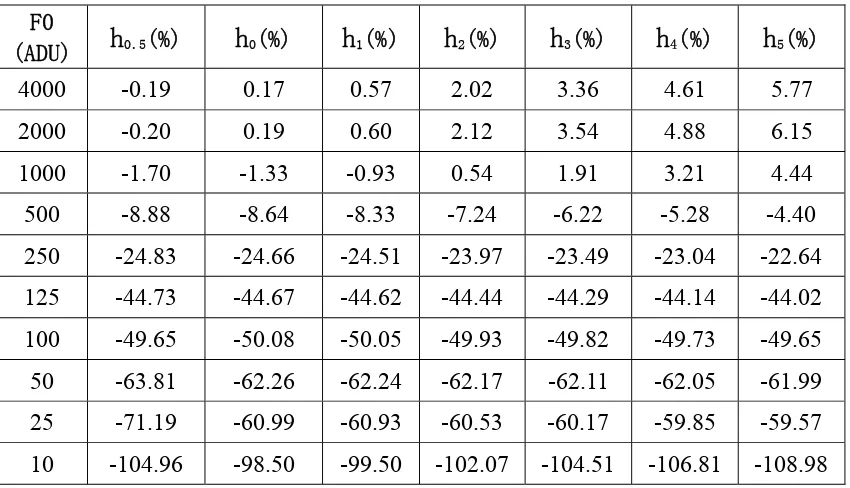
Table 3.1 Results of relative change of signal at different levels through inverse filtering.
F0
(ADU)
h
0.5(%)h
0(%)h
1(%)h
2(%)h
3(%)h
4(%)h
5(%)50 0.48 -0.53 -0.23 0.70 1.52 2.25 2.89 25 0.78 -1.68 -1.49 -4.17 -7.10 -10.27 -13.68 10 0.12 -1.70 -2.61 -8.40 -14.74 -21.64 -29.10
Table 3.2 Results of relative change of signal at different levels through Wiener filtering.
F0
(ADU)
h
0.5(%)h
0(%)h
1(%)h
2(%)h
3(%)h
4(%)h
5(%)4000 -0.19 0.17 0.57 2.02 3.36 4.61 5.77 2000 -0.20 0.19 0.60 2.12 3.54 4.88 6.15 1000 -1.70 -1.33 -0.93 0.54 1.91 3.21 4.44 500 -8.88 -8.64 -8.33 -7.24 -6.22 -5.28 -4.40 250 -24.83 -24.66 -24.51 -23.97 -23.49 -23.04 -22.64 125 -44.73 -44.67 -44.62 -44.44 -44.29 -44.14 -44.02 100 -49.65 -50.08 -50.05 -49.93 -49.82 -49.73 -49.65 50 -63.81 -62.26 -62.24 -62.17 -62.11 -62.05 -61.99 25 -71.19 -60.99 -60.93 -60.53 -60.17 -59.85 -59.57 10 -104.96 -98.50 -99.50 -102.07 -104.51 -106.81 -108.98
3.4
Simulation of the impact of IPC on SNR
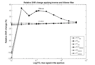
As a byproduct of the simulation on how IPC affects photometric measurement, the change of signal to noise ratio (SNR) was also studied. Equation 3.6 presents the formula used to calculate SNR. Similar to Figure 3.5, Figure 3.7 shows the performance comparison of inverse and Wiener filters in terms of SNR change for three tested filters
introduces less SNR change.
dark
N
N
S
S
SNR
pix rd
pix Aperture
Aperture
⋅
+
⋅
+
=
2σ
(3.6)where SApertureis the total signal with the selected aperture; σrdis readout noise per pixel;
is dark current signal per pixel; is the number of pixels in the aperture.
dark Npix
[image:62.612.116.510.271.544.2]Figure 3.7 Comparison of SNR change after applying the inverse and Wiener filters. Relative SNR change after deconvolution is refered to signal w/o IPC, SNR3 to SNR1_rd.
Table 3.3 Results of relative change of SNR at different levels through inverse filtering.
F0
(ADU)
h
0.5(%)h
0(%)h
1(%)h
2(%)h
3(%)h
4(%)h
5(%)2000 -1.16 -1.77 -1.62 -2.66 -3.82 -5.10 -6.50 1000 -1.66 -2.65 -2.52 -4.34 -6.26 -8.26 -10.33
[image:63.612.92.515.328.573.2]500 -2.17 -3.54 -3.44 -6.02 -8.63 -11.25 -13.89 250 -2.59 -4.26 -4.18 -7.34 -10.46 -13.53 -16.54 125 -2.95 -4.82 -4.77 -8.36 -11.84 -15.23 -18.51 100 -3.10 -5.02 -4.98 -8.67 -12.25 -15.71 -19.07 50 -2.25 -5.55 -5.56 -9.67 -13.59 -17.33 -20.91 25 -2.03 -6.76 -6.88 -14.22 -21.14 -27.67 -33.84 10 -2.72 -6.84 -8.00 -18.09 -27.68 -36.82 -45.55
Table 3.4 Results of relative change of SNR at different levels through Wiener filtering.
F0
(ADU)
h
0.5(%)h
0(%)h
1(%)h
2(%)h
3(%)h
4(%)h
5(%)4000 1.50 1.46 1.57 1.67 1.70 1.66 1.57 2000 5.10 5.08 5.18 5.25 5.27 5.27 5.23 1000 13.06 13.05 13.16 13.36 13.54 13.70 13.84
500 25.17 25.26 25.38 25.69 25.98 26.25 26.49 250 36.94 36.99 37.08 37.28 37.46 37.62 37.76 125 39.23 39.10 39.13 39.06 38.98 38.91 38.83 100 38.79 37.35 37.36 37.21 37.06 36.91 36.77 50 21.82 23.68 23.67 23.42 23.20 23.01 22.83 25 48.00 47.70 47.86 49.06 50.09 50.95 51.62 10 -117.16 -98.19 -102.20 -111.76 -120.69 -129.00 -136.69
with a big coupling always made the relative SNR change large, as shown in Figure 3.8. This may be explained as the deconvolution is a sharpening process according to those kernels we used. The operation of deconvolution sharpened not only the image but the noise. Bigger coupling would cause a larger noise sharpening and thus a smaller SNR.
Figure 3.8 Relative SNR change at different signal levels after inverse filter was applied. Relative SNR change after deconvolution is refered to signal w/o IPC, SNR3 to SNR1_rd.
3.5
Summary
4
Interpixel coupling and read noise
It is widely believed that IPC occurs in the space between the detector array and multiplexer between indium bumps (Finger et al. 2006, Brown et al. 2006, Bai et al. 2007). In Si-PIN detectors, coupling can also exist in the diode array between photodiodes. Both of the two mechanisms suggest that interpixel coupling occurs before read noise is introduced. Besides the detector array and the space between indium bump interconnects, mutual capacitance may also occur inside the readout integrated circuit (ROIC), where the noise signal may couple capacitively to their neighbors (Brown et al. 2007). If this occurs, the readout noise would be attenuated in a similar fashion to Poisson noise, and become spatially correlated. This chapter will address the read noise related coupling.
4.1
Read noise
related to the measuring systems since any instrument has certain uncertainties. Therefore, readout noise can be reduced to an acceptable level by optimized design.
4.2
Modeling of read noise and IPC
To investigate the read noise related coupling, we focus on images that are dominated by read noise. To this end, bias frames, dark frames with minimum exposure, are used. A bias frame can be expressed as follows if the read noise is not polluted by capacitive coupling.
]
,
[
]
,
[
]
,
[
]
,
[
i
j
offset
i
j
dark
mini
j
readnoise
i
j
bias
=
+
+
(4.1)where the signal of each pixel is composed of the offset, minimum dark signal, and readout noise. Ideally, read noise is spatially uncorrelated between adjacent pixels. If interpixel coupling affects read noise in the same manner to photon noise discussed in Chap. 1 and 2, readout noise will be smoothed. Thus Eq. 4.1 is rewritten as follows.
(
[
,
]
[
,
]
[
,
]
)
*
[
,
]
]
,
[
i
j
offset
i
j
dark
mini
j
readnoise
i
j
h
i
j
bias
=
+
+
ipc (4.2)Interpixel coupling is modeled as a low-pass convolution kernel as discussed in
previous sections. Note that the coupling magnitude here should be smaller than interpixel coupling measured by cosmic ray events or hot pixels as only the coupling from within the multiplexer and even post-readout circuitry is considered, whereas the coupling discussed before comes from the space between photodiode array and
multiplexer between In bumps, and between neighboring photodiodes. Neglecting minimum dark signal and differencing two bias frames, we obtain
] , [ * ]) , [ 2 ] , [ 1 ([ ] , [ 2 ] , [ 1 ] ,
[i j bias i j bias i j readnoise i j readnoise i j h i j
D = − = − ipc (4.3)
where is the difference of two bias frames. The difference of any two bias
frames cancels out the offset, leaving only the difference of read noise, whose variance is twice the variance of the original readout noise component.
] , [i j D
The autocorrelation of the difference image is equal to the correlation of impulse response with itself, scaled by the variance of read noise component in the bias frames, as shown below.
]
,
[
*
]
,
[
2
]
,
[
x
y
2h
x
y
h
x
y
R
D=
σ
RD ipc ipc−
−
(4.4)If interpixel coupling does not exist among read noise, equals an ideal 2-D
delta function
] , [x y hipc
]
,
[
x
y
δ
. The resulting autocorrelation function will not present any term inFigure 4.1 Left: autocorrelation of an ideal Gaussian noise image with zero mean and σ = 5 DN; right: autocorrelation of same noise image but convolved with a low-pass filter.
To check whether the read noise is affected by capacitive coupling, we analyzed the bias frames taken from two typ